EP0513831B1 - Procédé d'utilisation de fondant, de circuit imprimé et son procédé de fabrication - Google Patents
Procédé d'utilisation de fondant, de circuit imprimé et son procédé de fabrication Download PDFInfo
- Publication number
- EP0513831B1 EP0513831B1 EP19920108285 EP92108285A EP0513831B1 EP 0513831 B1 EP0513831 B1 EP 0513831B1 EP 19920108285 EP19920108285 EP 19920108285 EP 92108285 A EP92108285 A EP 92108285A EP 0513831 B1 EP0513831 B1 EP 0513831B1
- Authority
- EP
- European Patent Office
- Prior art keywords
- treatment
- printed wiring
- preflux
- wiring board
- reflow
- Prior art date
- Legal status (The legal status is an assumption and is not a legal conclusion. Google has not performed a legal analysis and makes no representation as to the accuracy of the status listed.)
- Expired - Lifetime
Links
- 0 *C1=NC(CCCC2)C2N1 Chemical compound *C1=NC(CCCC2)C2N1 0.000 description 1
Images


Classifications
-
- B—PERFORMING OPERATIONS; TRANSPORTING
- B23—MACHINE TOOLS; METAL-WORKING NOT OTHERWISE PROVIDED FOR
- B23K—SOLDERING OR UNSOLDERING; WELDING; CLADDING OR PLATING BY SOLDERING OR WELDING; CUTTING BY APPLYING HEAT LOCALLY, e.g. FLAME CUTTING; WORKING BY LASER BEAM
- B23K35/00—Rods, electrodes, materials, or media, for use in soldering, welding, or cutting
- B23K35/22—Rods, electrodes, materials, or media, for use in soldering, welding, or cutting characterised by the composition or nature of the material
- B23K35/36—Selection of non-metallic compositions, e.g. coatings, fluxes; Selection of soldering or welding materials, conjoint with selection of non-metallic compositions, both selections being of interest
- B23K35/3612—Selection of non-metallic compositions, e.g. coatings, fluxes; Selection of soldering or welding materials, conjoint with selection of non-metallic compositions, both selections being of interest with organic compounds as principal constituents
- B23K35/3615—N-compounds
-
- H—ELECTRICITY
- H05—ELECTRIC TECHNIQUES NOT OTHERWISE PROVIDED FOR
- H05K—PRINTED CIRCUITS; CASINGS OR CONSTRUCTIONAL DETAILS OF ELECTRIC APPARATUS; MANUFACTURE OF ASSEMBLAGES OF ELECTRICAL COMPONENTS
- H05K1/00—Printed circuits
-
- C—CHEMISTRY; METALLURGY
- C23—COATING METALLIC MATERIAL; COATING MATERIAL WITH METALLIC MATERIAL; CHEMICAL SURFACE TREATMENT; DIFFUSION TREATMENT OF METALLIC MATERIAL; COATING BY VACUUM EVAPORATION, BY SPUTTERING, BY ION IMPLANTATION OR BY CHEMICAL VAPOUR DEPOSITION, IN GENERAL; INHIBITING CORROSION OF METALLIC MATERIAL OR INCRUSTATION IN GENERAL
- C23F—NON-MECHANICAL REMOVAL OF METALLIC MATERIAL FROM SURFACE; INHIBITING CORROSION OF METALLIC MATERIAL OR INCRUSTATION IN GENERAL; MULTI-STEP PROCESSES FOR SURFACE TREATMENT OF METALLIC MATERIAL INVOLVING AT LEAST ONE PROCESS PROVIDED FOR IN CLASS C23 AND AT LEAST ONE PROCESS COVERED BY SUBCLASS C21D OR C22F OR CLASS C25
- C23F11/00—Inhibiting corrosion of metallic material by applying inhibitors to the surface in danger of corrosion or adding them to the corrosive agent
- C23F11/08—Inhibiting corrosion of metallic material by applying inhibitors to the surface in danger of corrosion or adding them to the corrosive agent in other liquids
- C23F11/10—Inhibiting corrosion of metallic material by applying inhibitors to the surface in danger of corrosion or adding them to the corrosive agent in other liquids using organic inhibitors
- C23F11/14—Nitrogen-containing compounds
- C23F11/149—Heterocyclic compounds containing nitrogen as hetero atom
-
- H—ELECTRICITY
- H05—ELECTRIC TECHNIQUES NOT OTHERWISE PROVIDED FOR
- H05K—PRINTED CIRCUITS; CASINGS OR CONSTRUCTIONAL DETAILS OF ELECTRIC APPARATUS; MANUFACTURE OF ASSEMBLAGES OF ELECTRICAL COMPONENTS
- H05K3/00—Apparatus or processes for manufacturing printed circuits
- H05K3/22—Secondary treatment of printed circuits
- H05K3/28—Applying non-metallic protective coatings
- H05K3/282—Applying non-metallic protective coatings for inhibiting the corrosion of the circuit, e.g. for preserving the solderability
-
- H—ELECTRICITY
- H05—ELECTRIC TECHNIQUES NOT OTHERWISE PROVIDED FOR
- H05K—PRINTED CIRCUITS; CASINGS OR CONSTRUCTIONAL DETAILS OF ELECTRIC APPARATUS; MANUFACTURE OF ASSEMBLAGES OF ELECTRICAL COMPONENTS
- H05K3/00—Apparatus or processes for manufacturing printed circuits
- H05K3/30—Assembling printed circuits with electric components, e.g. with resistor
- H05K3/32—Assembling printed circuits with electric components, e.g. with resistor electrically connecting electric components or wires to printed circuits
- H05K3/34—Assembling printed circuits with electric components, e.g. with resistor electrically connecting electric components or wires to printed circuits by soldering
- H05K3/3489—Composition of fluxes; Methods of application thereof; Other methods of activating the contact surfaces
-
- H—ELECTRICITY
- H05—ELECTRIC TECHNIQUES NOT OTHERWISE PROVIDED FOR
- H05K—PRINTED CIRCUITS; CASINGS OR CONSTRUCTIONAL DETAILS OF ELECTRIC APPARATUS; MANUFACTURE OF ASSEMBLAGES OF ELECTRICAL COMPONENTS
- H05K2203/00—Indexing scheme relating to apparatus or processes for manufacturing printed circuits covered by H05K3/00
- H05K2203/05—Patterning and lithography; Masks; Details of resist
- H05K2203/0562—Details of resist
- H05K2203/0591—Organic non-polymeric coating, e.g. for inhibiting corrosion thereby preserving solderability
-
- Y—GENERAL TAGGING OF NEW TECHNOLOGICAL DEVELOPMENTS; GENERAL TAGGING OF CROSS-SECTIONAL TECHNOLOGIES SPANNING OVER SEVERAL SECTIONS OF THE IPC; TECHNICAL SUBJECTS COVERED BY FORMER USPC CROSS-REFERENCE ART COLLECTIONS [XRACs] AND DIGESTS
- Y10—TECHNICAL SUBJECTS COVERED BY FORMER USPC
- Y10S—TECHNICAL SUBJECTS COVERED BY FORMER USPC CROSS-REFERENCE ART COLLECTIONS [XRACs] AND DIGESTS
- Y10S428/00—Stock material or miscellaneous articles
- Y10S428/901—Printed circuit
-
- Y—GENERAL TAGGING OF NEW TECHNOLOGICAL DEVELOPMENTS; GENERAL TAGGING OF CROSS-SECTIONAL TECHNOLOGIES SPANNING OVER SEVERAL SECTIONS OF THE IPC; TECHNICAL SUBJECTS COVERED BY FORMER USPC CROSS-REFERENCE ART COLLECTIONS [XRACs] AND DIGESTS
- Y10—TECHNICAL SUBJECTS COVERED BY FORMER USPC
- Y10T—TECHNICAL SUBJECTS COVERED BY FORMER US CLASSIFICATION
- Y10T428/00—Stock material or miscellaneous articles
- Y10T428/24—Structurally defined web or sheet [e.g., overall dimension, etc.]
- Y10T428/24802—Discontinuous or differential coating, impregnation or bond [e.g., artwork, printing, retouched photograph, etc.]
- Y10T428/24917—Discontinuous or differential coating, impregnation or bond [e.g., artwork, printing, retouched photograph, etc.] including metal layer
-
- Y—GENERAL TAGGING OF NEW TECHNOLOGICAL DEVELOPMENTS; GENERAL TAGGING OF CROSS-SECTIONAL TECHNOLOGIES SPANNING OVER SEVERAL SECTIONS OF THE IPC; TECHNICAL SUBJECTS COVERED BY FORMER USPC CROSS-REFERENCE ART COLLECTIONS [XRACs] AND DIGESTS
- Y10—TECHNICAL SUBJECTS COVERED BY FORMER USPC
- Y10T—TECHNICAL SUBJECTS COVERED BY FORMER US CLASSIFICATION
- Y10T428/00—Stock material or miscellaneous articles
- Y10T428/31504—Composite [nonstructural laminate]
- Y10T428/31678—Of metal
- Y10T428/31681—Next to polyester, polyamide or polyimide [e.g., alkyd, glue, or nylon, etc.]
Definitions
- This invention relates to a method for improving the heat proofness and chemical resistance or preflux to be used as for soldering metals. It further relates to a printed wiring board which, in the operation of mounting electronic parts in high density on the opposite surfaces of the printed wiring board and reflow soldering them to the surfaces, allows the surfaces thereof to be wetted thoroughly with the solder and enables the soldering inside through holes formed therein to be carried out with enhanced efficiency and to a method for the production of the printed wiring board.
- the prefluxes which have been heretofore used for the purpose of rustproofing circuit parts of copper or copper alloy formed on a printed wiring board and intended to be soldered and retaining the circuit parts in a solderable state are broadly divided into two kinds, i.e. a resin type preflux intended to coat a printed wiring board wholly and an alkylimidazole type preflux intended to produce a chemical reaction selectively with the copper or copper alloy.
- the former preflux is used by a method which comprises dissolving natural rosin, rosin ester, or rosin-modified maleic acid resin in an organic solvent, applying the resultant solution to a whole printed wiring board by spraying with a roll coater, immersion, or the combination thereof, and drying the applied layer of the solution thereby forming a film coating the printed wiring board.
- the resin type preflux owing to the use of the organic solvent, entails the disadvantage that the solvent evaporates into the ambient air and seriously jeopardizes environment and safety.
- the alkylimidazole type preflux is soluble in water and excels in point of work environment and safety. It nevertheless entails the disadvantage that an alkylimidazole copper complex arising from the reaction of the preflux with the copper or copper alloy of the printed wiring board, on exposure to an elevated temperature, is decomposed and degenerated by the catalytic action of oxygen in the air and copper and consequently suffered to adhere fast to the circuit of copper or copper alloy, impede the action of a postflux, and impair the solderability of the circuit.
- the printed wiring board is produced by a method which comprises applying the alkylimidazole type preflux to the printed wiring board and then reflow soldering electronic parts to the surfaces of the printed wiring board thereby effecting desired mounting of the electronic parts on the printed wiring board.
- the reflow soldering techniques which have been developed to date to the level of commercialization and actually adopted for mounting electronic parts on the surfaces of a printed wiring board include air reflow, infrared reflow, near-infrared reflow, reflow of the type combining air reflow and infrared reflow, reflow performed in the atmosphere of nitrogen, and vapor reflow for performing soldering in the vapor phase of perfluorocarbon, for example.
- the alkylimidazole type preflux When the alkylimidazole type preflux is applied to a surface as described above and then the reflow soldering is performed on the coated surface, the preflux which is consequently exposed to an elevated temperature poses the problem of heatproofness and chemical resistance.
- the surface of copper and copper alloy is invaded by a halogenide contained in a cream solder which is used as a solder and the moisture evaporating from within a printed wiring and the evaporating moisture goes to decomposing the perfluorocarbon, though only to a slight extent, with liberation of hydrofluoric acid and inevitably inducing corrosion of the surface of copper, with the result that the susceptibility of the surface to wetting with the solder during the process or reflow soldering, the efficiency of the soldering work performed subsequently to the step of reflowing in through holes formed in the printed wiring board, and the susceptibility of the through holes to wetting with the solder are degraded.
- the inventors in the light of the problem mentioned above, continued a study in search of a metal soldering grade preflux endowed with improved heatproofness and chemical resistance, a printed wiring board susceptible to perfect wetting with solder even after two to three rounds of reflow soldering and capable of undergoing soldering with enhanced efficiency, and a method for the production of this printed wiring board.
- the first object of this invention is to provide a method for improving the heat proofness, chemical resistance and the soldering efficiency of preflux treated metals.
- the second object of this invention is to provide a printed wiring board which produces a prominent effect of imparting improved solderability to the reflow to be used in mounting electronic parts on the surfaces of the printed wiring board and, as a result, enhancing the mounting density of electronic parts on the printed wiring board, and contributing to the miniaturization of electronic devices.
- the third object of this invention is to provide a method for the production of a printed wiring board which is capable of imparting improved solderability to the reflow being used in mounting electronic parts on the surfaces of the printed wiring board.
- the present invention provides a method for improving the heat proofness, chemical resistance and the soldering efficiency of preflux treated metals, intended to be soldered, whereby the preflux contains as an active component an imidazole type compound represented by the following general formula: (wherein R 1 stands for H or an alkyl group of three to 17 carbon atoms, R 2 for H or an alkyl group of one to six carbon atoms, and n for an integer in the range between 0 and 3) or the following general formula (2); (wherein R3 stands for H or an alkyl group of one to six carbon atoms, R4 for H or an alkyl group of one to six carbon atoms, R5 for an alkyl group of zero to seven carbon atoms, and n for an integer in the range between 0 and 3) or the following general formula (3); (wherein R stands for H or an alkyl group of one to 17 carbon atoms and R' for H or an alkyl group of one to three carbon atoms) or the following general formula (4)
- the preflux treated metals are printed wiring boards on which circuits have been formed.
- the present invention provides printed wiring boards which have been treated according to the above method.
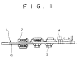
- a printed wiring board 1 has electronic parts 2 and 3 for mounting and a lead insertion part 4 for mounting severally mounted as illustrated in Fig. 1 on the opposite surfaces for mounting of a printed wiring board proper 1a.
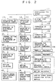
- Fig. 2 is a diagram illustrating a process for the production of a printed wiring board (with copper through holes) of this invention.
- the printed wiring board proper 1a is subjected to perforation (101) for the formation of holes therein and the holes are finished by plating (102) for the formation of through holes.
- circuits in a prescribed wiring pattern are formed (103) and a solder resist is formed by printing (104).
- the printed wiring board proper 1a is subjected to outline machining (105) for the impartation of outline dimensions thereto and to a preflux treatment (106).
- an oxidizing treatment (107) for the oxidation of the preflux applied to the printed wiring board 1a is carried out. This step completes the production of the printed wiring board 1.
- the printed wiring board is finished for practical service (111) by applying solder cream (108) to the surfaces of the printed wiring board 1 obtained as described above, mounting the electronic parts 2 and 3 (109), and carrying out the step of reflow soldering (110).
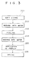
- Fig. 3 is a diagram illustrating a detailed process for the preflux treatment (106) shown in Fig. 2.
- the process starts with a soft etching treatment (201) by 20 to 30 seconds' immersion of the printed wiring board proper 1a in an aqueous solution containing 200 g of sodium persulfate per liter and kept at 30°C. Then, the printed wiring board proper 1a is subjected to a treatment of water washing (202).
- the printed wiring board proper 1a is subjected to a pickling treatment (203) by 20 seconds' immersion in an aqueous solution containing 3% of hydrochloric acid and held at normal room temperature. This treatment is followed by a treatment (204) for washing the printed wiring board proper 1a with water.
- the washed print wiring board proper 1a is then subjected to a preflux treatment (205) by 60 to 80 seconds' immersion thereof in a solution containing benzimidazole or benzimidazole derivative represented by the general formula (1), preferably by the following general formula (3), or benzimidazole represented by the general formula (2), preferably by the following general formula (4) or an example of a derivative of benzimidazole, Docoat H produced by Sanwa Laboratory, and kept at 45°C and consequent attachment (application) to the surface of copper of the printed wiring board proper 1a of a preflux resulting from a chemical reaction.
- the printed wiring board which has undergone the preflux treatment (205) is subjected to a drying treatment (206) under the conditions of 80°C and 30 to 40 seconds.
- R stands for H or an alkyl group of one to 17 carbon atoms and R' for H or an alkyl group of one to three carbon atoms).
- R'' stands for H or an alkyl group of zero to three carbon atoms.
- the first example of this oxidizing treatment consists in a heat treatment to be performed in an atmosphere of air, the second example thereof in a treatment with a chemical solution, and the third example thereof in a treatment of exposure to ozone (O 3 ).
- the printed wiring board 1 produced by the process described above was tested to find how the oxidizing treatment performed after the application of preflux would improve the heatproofness and chemical resistance of the preflux.
- the results were as follows. In due consideration of the heatproofness and chemical resistance of the reflow solder, a vapor reflow treatment (passage of the printed wiring board 1 having no solder paste applied thereto through a treating tank intended for the vapor flow treatment) was perfomed twice and the outcome of this treatment was rated by the fraction defective of the solder after the step of flow dip soldering.
- the conditions for the flow dip soldering were postflux, JS-64P, specific gravity between 0.84 and 0.86, soldering temperature 245°C, and soldering time three seconds.
- Fig. 4 shows the fraction defective of the soldering work in a heat treatment carried out at varying temperatures of 80, 100, 120, and 150°C for varying durations of 1, 5, and 10 minutes.
- samples of the printed wiring board 1 which had undergone the preflux treatment with Docoat H produced by Sanwa Laboratory were severally treated in aqueous solutions containing hydrogen peroxide in varying concentrations of 1, 5, and 10% invariably at normal room temperature for varying periods or 1, 5, and 10 minutes.
- the treatment by exposure to ozone (O 3 ) to be performed as the third example of the oxidizing treatment brings about entirely the same effect of improving the heatproofness and chemical resistance of the preflux.
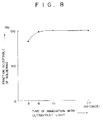
- Fig. 8 The case of performing a treatment by irradiation with the ultraviolet light is depicted in Fig. 8 as the fourth example of the oxidizing treatment.
- an ultraviolet lamp produced by Japan Storage Battery Co., Ltd. and rated for an electric power of 120 W/cm was used and samples of the printed wiring board were severally exposed to the light from the lamp for varying periods of 3, 6, 10, and 20 seconds to find fraction defectives of the soldering work. It has been found that the treatment time of about 10 seconds produces a fraction acceptable of 100% and effectively improves the heatproofness and chemical resistance.
- the heatproofness and chemical resistance of the preflux is conspicuously improved by the method which comprises subjecting the printed wiring board 1 which has undergone the treatment for the formation of circuits thereon to the preflux treatment (106) shown in Fig. 2 using benzimidazole or benzimidazole derivative represented by the general formula (1), preferably the general formula (3), or benzimidazole or benzimidazole derivative represented by the general formula (2), preferably by the general formula (4), such as a proprietary product or Sanwa Laboratory marketed under trademark designation of "Docoat H," thereby causing the preflux to react upon copper or copper alloy and then performing the oxidizing treatment (107).
- benzimidazole or benzimidazole derivative represented by the general formula (1) preferably the general formula (3)
- benzimidazole or benzimidazole derivative represented by the general formula (2) preferably by the general formula (4), such as a proprietary product or Sanwa Laboratory marketed under trademark designation of "Docoat H," thereby causing the pref
- the oxidizing treatment mentioned above to be performed subsequently to the preflux treatment (106) in the form of a heat treatment, for example, at a varying temperature in the range between 100 and 150°C for a varying period in the range between one and 10 minutes is effective in lowering the fraction defective to 1/7 to 1/30 of that of the untreated sample.
- This heat treatment can be easily accomplished by causing the printed wiring board 1 which has undergone the preflux treatment to be treated with a constant temperature bath or a conveyor type drying oven.
- the oxidizing treatment is effectively obtained subsequently to the preflux treatment by a treatment with a chemical solution such as, for example, an aqueous 1% hydrogen peroxide at normal room temperature for five minutes.
- a chemical solution such as, for example, an aqueous 1% hydrogen peroxide at normal room temperature for five minutes.
- This treatment decreases the fraction defective of the soldering work to 1/7 of that of the untreated sample. This fact indicates that the treatment with the chemical solution is capable of prominently enhancing the heatproofness and chemical resistance of the preflux.
- oxidizing treatment use of an aqueous 2% Ca(Cl0) 2 ⁇ 3H 2 O solution is as effective as the use of the aqueous hydrogen peroxide solution mentioned above.
- This oxidizing treatment can be easily accomplished by immersing the printed wiring board in a bath of the chemical solution by shower spraying the chemical solution on the printed wiring board.
- the oxidizing treatment can be as effectively performed subsequently to the preflux treatment by a treatment of exposure of the printed wiring board 1 to an atmosphere of ozone as by the treatment with the chemical solution.
- This treatment is easily performed by the use of a chamber adapted for the ozone treatment and brings about a conspicuous improvement in the heatproofness and chemical resistance of the printed wiring board.
- a heat treatment (performed at a temperature in the range between 120 and 150°C for a period in the range between one and five minutes, for example) preparatory to the reflow treatment, i.e. a heat treatment given to the printed wiring board produced in consequence or the process of steps 112 through 118 and steps 119 through 125 shown in Figs. 2 (a) and (b) in the open air in an atmosphere of oxygen during the step for mounting electronic parts, brings about the same effect as shown in Fig. 4.
- This heat treatment lowers the fraction defective of the soldering work to 1/7 to 1/30 of that of the untreated sample. It can prominently improve the heatproofness and chemical resistance of the printed wiring board.
- solder cream is applied (112) to the surface of the printed wiring board 1 which has undergone the preflux treatment (106) and has been readied for mounting of electronic parts, the elevtronic parts are mounted (113) on the solder-coated surface, the solder cream is applied (115) to the other surface of the printed wiring board 1 for mounting other electronic parts, the electronic parts are mounted (116) on the solder-coated surface, and reflow soldering (117) is performed to complete a printed wiring board for actual service (118).
- adhesive agent is applied (119) to the surface of the printed wiring board 1 which has undergone the preflux treatment (106) and has been readied for mounting electronic parts, the electronic parts are mounted (120) to the adhesive-coated surface, solder cream is applied (122) to the other surface of the printed wiring board 1 for mounting electronic parts, the electronic parts are mounted (123) on the solder-coated surface, and reflow soldering (124) is performed, to complete the printed wiring board (125) for actual service.
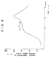
- Fig. 6 illustrates a temperature profile which is drawn during a reflow treatment with infrared light
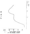
- Fig. 7 illustrates a temperature profile which is drawn during a vapor reflow treatment.
- the region indicated by H represents the duration for the oxidizing treatment.
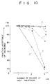
- a copper through hole printed wiring board was prepared, treated with preflux (produced by Sanwa Laboratory and marketed under trademark designation of "Docoat H"), and subjected to an oxidizing treatment at 150°C for five minutes, to produce Sample A conforming to this invention.
- Sample B was produced by following the procedure described above, excepting the oxidizing treatment was omitted, and Sample C was produced by the resin type preflux treatment which is in widespread use.
- a treatment of passage througha reflow treating tank in the vapor phase of perfluorocarbon was performed one to three times on Samples A, B, and C and the samples were subjected to flow dip soldering. The copper through holes of these samples were examined to evaluate the outcome of the soldering work.
- Fig. 10 shows the relation between the number of heat treatments and the fraction acceptable of the soldering work.
- the oxidizing treatment enabled Sample A to acquire conspicuously improved fraction acceptable of the soldering work as compared with Sample B which escaped the oxidizing treatment. This fact indicates that the oxidizing treatment is notably effective in enhancing heatproofness and chemical resistance. This effect is prominent over that of Sample C which used the resin type preflux.
- Sample A' was produced by using a preflux of Docoat H and performing the oxidizing treatment in the form of a heat treatment carried out in an atmosphere of air preparatorily to the infrared reflow and sample C' was produced by the resin type preflux treatment.
- a treatment of passage through a tank for an infrared reflow treatment in an atmosphere of air was performed one to three times on these samples. The results were as shown in Fig. 10.
- the copper on the printed wiring board a was given a preflux treatment with Docoat H produced by Sanwa Laboratory.
- the printed wiring board was subjected to a varying treatment indicated in the group of steps represented by conditions 1 to 8, and finally subjected to flow dip soldering. It was then tested for acceptability of the soldering work.
- conditions 1 to 4 represent the cases in which the reflow was carried out without the oxidizing treatment
- Conditions 5 to 8 the cases in which the oxidizing treatment was carried out in the form of a heat treatment performed under varying conditions of 120 to 150°C of temperature and one to five minutes of time preparatorily to the infrared reflow in an atmosphere of air.
- This invention therefore, is exceptionally effective in realizing high-density mounting of electronic parts on the opposite surfaces of the printed wiring board and also is amply effective in point of correction of the reflow solder and replacement of parts.
- FIGs. 12 A process for forming a benzimidazole copper complex film 7 on the surfaces of copper or copper alloy through holes 5 and copper or copper alloy patterns 6 of the printed wiring board 1 when the oxidizing treatment is performed on the printed wiring board 1 after the preflux treatment is depicted in Figs. 12 (a), (b), and (c).
- the printed wiring board 1 provided with copper or copper alloy through holes 5 and copper or copper alloy patterns 6 is subjected to a preflux treatment so as to form, as illustrated in Fig. 12 (b), on the surfaces of the copper or copper alloy through holes 5 and the copper a copper alloy patterns 6 a film 8 of 2-alkylbenzimidazole or 2-alkylbenzimidazole derivative represented by the general formula (3) or 2-phenylbenzaimidazole or 2-phenylbenzimidazole derivative represented by the general formula (4) and thereafter subjected to the oxidizing treatment so as to convert, as illustrated in Fig. 12 (c), the film 8 on the surfaces of the copper or copper alloy through holes 5 and the copper or copper alloy patterns 6 into a film of benzimidazole copper complex 7.
- the surface of copper plate was treated by immersion in a preflux solution prepared by dissolving 0.5% of 2-n-nonylbenzimidazole, 3% of an organic acid, and 100 ppm of copper ion in water at about 40°C for a period in the range between 30 and 60 seconds and of the film on the copper surface was analyzed by the X-ray photoelectric spectrometry to detect possible change in the structure thereof.
- the raw materials used for this analysis were as follows.
- the amounts of the functional groups present therein are shown in the following table.
- Sample -N (399.9eV) -NH-(398.4eV) N-Cu (399.0ev)
- the oxidizing treatment such as, for example, a heat treatment in the open air at 120°C for five minutes or a heat treatment in the open air at 230°C for three minutes brought about substantial absence of the free imidazole group and increase of the amount of benzimidazole copper complex to 96% or 97%, with the result that the reaction for the formation of the complex thoroughly proceeded to give rise to a film of benzimidazole copper complex.
- the formation of the film of benzimidazole copper complex 7 in the manner described above produces a conspicuous effect of enhancing the solderability of reflow for the mounting of electronic parts on the printed wiring board 1. It also allows improvement of the density of mounting on the printed wiring board 1 and contributes to miniaturization of electronic devices.
- the heatproofness and chemical resistance of the printed wiring board can be conspicuously improved by performing a preflux treatment on copper or copper alloy by the use of benzimidazole or benzimidazole derivative represented by the general formula (1) or benzimidazole or benzimidazole derivative represented by the general formula (2) and then subjecting the outcome of the proflux treatment to the oxidizing treatment as described in detail above.
- the printed wiring board contemplated by this invention produces a prominent effect of improving the solderability of reflow during the mounting of electronic parts on the printed wiring board because the oxide film has been formed on the metallic surface of the printed wiring board for mounting of electronic parts by applying the preflux represented by the general formula (1) or the general formula (2) to the printed wiring board on which circuits have been already formed and then subjecting the resultant preflux-coated printed wiring board to the oxidizing treatment.
- this invention can enhance the density of mounting on the printed wiring board and contributes to miniaturization of electronic devices.
- the method of this invention for the production of the printed wiring board is capable of producing a printed board which enjoys high fraction acceptable of the printing work and ample wettability and excels in point of work environment and safety because it comprises applying a preflux represented by the general formula (1) or the general formula (2) to the printed wiring board on which circuits have been already formed and then subjecting the preflux-coated printed wiring board to the oxidizing treatment.
- the method of this invention for the production of the printed wiring board is characterized by appling a preflux represented by the general formula (1) or the general formula (2) to the printed wiring board on which circuits have been already formed and then subjecting the preflux-coated printed wiring board to the reflow treatment which is performed in the form of a heat treatment in the air or in an atmosphere of oxygen.
- the reflow treatment includes infrared reflow treatment at least in the initial stage thereof, it brings about an effect of attaining the oxidation of the preflux without requiring any independent oxidizing treatment subsequently to the preflux treatment in the process of production of the printed wiring board in addition to the effect derivable by the aforementioned method for production of the printed wiring board.
- the heatproofness and chemical resistance of the printed wiring board can be conspicuously improved by performing the preflux treatment on copper or copper alloy by the use of 2-alkylbenzimidazole or 2-alkylbenzimidazole represented by the general formula (3) or 2-phenylbenzimidazole or 2-phenylbenzimidazole derivative represented by the general formula (4) and then subjecting the outcome of the preflux treatment to the oxidizing treatment.
- the printed wiring board contemplated by this invention brings about a prominent effect of improving the solderability of reflow in the mounting of electronic parts on the printed wiring board because it has the film of benzimidazole copper complex on the metallic surface of the printed wiring board for mounting by a procedure which comprises applying the preflux represented by the general formula (3) or the general formula (4) to the printed wiring board on which circuits have been already formed and subjecting the preflux-coated printed wiring board to the oxidizing treatment. It is also capable of enhancing the density of mounting on the printed wiring board and contributing to miniaturization of electronic devices.
- the method for the production or a printed wiring board contemplated by this invention is characterized by applying the preflux represented by the general formula (3) or the general formula (4) to the printed wiring board on which circuits have been already formed and then subjecting the preflux-coated printed wiring board to a reflow treatment which consists in applying heat thereto in the air or in an atmosphere of oxygen.
- a reflow treatment which includes an infrared reflow treatment at least in the initial stage thereof, it is capable of bringing about an effect of realizing the oxidation or the preflux without requiring any independent oxidizing treatment subsequently to the preflux treatment in the process for production of the printed wiring board in addition to the effect produced by the method for production of the printed wiring board.
- Fig. 1 is a side view illustrating part of a printed wiring board produced by mounting electronic parts on a printed wiring board proper in according to this invention.
- Fig. 2 is a flow chart representing a process for the production of a printed wiring board in accordance with this invention.
- Fig. 3 is a flow chart representing the step of preflux treatment in the process for the production of a printed wiring board in accordance with this invention.
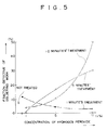
- Fig. 4 is a graph showing the relation between the temperature of the heat treatment performed by way of oxidizing treatment in an atmosphere of air and the fraction defective of the soldering work.
- Fig. 5 is a graph showing the relation between the concentration of hydrogen peroxide and the fraction defective of the soldering work in the treatment with chemical solution which is intended as an oxidizing treatment.
- Fig. 6 is a graph showing a temperature profile obtained in an infrared reflow treatment.
- Fig. 7 is a graph showing a temperature profile obtained in a vapor reflow treatment.
- Fig. 8 is a graph showing a fraction defective of the soldering work performed in an ultraviolet irradiation treatment intended as an oxidizing treatment.
- Fig. 9 is a graph showing a temperature profile obtained in a vapor reflow treatment.
- Fig. 10 is a graph showing the relation between the number of heat treatments performed one to three times in the infrared reflow treatment in an atmosphere of air and the fraction defective of the soldering work.
- Fig. 11 is a graph showing the relation between the condition for the flow dip soldering selected from the group of conditions 1 to 8 and performed on the copper of a printed wiring board subsequently to the preflux treatment and the fraction defective of the soldering work.
- Fig. 12 (a) is a cross section of part of a printed wiring board provided with copper or copper alloy through holes and copper or copper alloy patterns.
- Fig. 12 (b) is an explanatory diagram illustrating the outcome of the preflux treatment performed on the printed wiring board.
- Fig. 12 (c) is an explanatory diagram illustrating the outcome of the oxidizing treatment performed on the printed wiring board which has undergone the preflux treatment.
Landscapes
- Engineering & Computer Science (AREA)
- Microelectronics & Electronic Packaging (AREA)
- Manufacturing & Machinery (AREA)
- Mechanical Engineering (AREA)
- Chemical & Material Sciences (AREA)
- Materials Engineering (AREA)
- Metallurgy (AREA)
- Organic Chemistry (AREA)
- Electric Connection Of Electric Components To Printed Circuits (AREA)
- Preventing Corrosion Or Incrustation Of Metals (AREA)
- Non-Metallic Protective Coatings For Printed Circuits (AREA)
- Manufacturing Of Printed Wiring (AREA)
Claims (3)
- Procédé pour l'amélioration de la résistance à la chaleur, de la résistance chimique et de l'efficacité de brasage de métaux traités avec un préflux, destinés à être brasés, dans lequel le préflux contient comme composant actif un composé de type imidazole représenté par la formule générale suivante :(dans laquelle R1 représente un atome d'hydrogène ou un groupe alkyle de trois à 17 atomes de carbone, R2 représente un atome d'hydrogène ou un groupe alkyle de un à six atomes de carbone, et n un entier dans l'intervalle entre 0 et 3)

ou la formule générale (2) suivante :(dans laquelle R3 représente un atome d'hydrogène ou un groupe alkyle de un à six atomes de carbone, R4 représente un atome d'hydrogène ou un groupe alkyle de un à six atomes de carbone, R5 représente un groupe alkyle de zéro à sept atomes de carbone, et n un entier dans l'intervalle entre 0 et 3)
ou la formule générale (3) suivante :(dans laquelle R représente un atome d'hydrogène ou un groupe alkyle de un à 17 atomes de carbone et R' représente un atome d'hydrogène ou un groupe alkyle de un à trois atomes de carbone)
ou la formule générale (4) suivante :(dans laquelle R'' représente un atome d'hydrogène ou un groupe alkyle de zéro à trois atomes de carbone).
par lequel, après avoir déposé le préflux sur la surface du métal, on effectue un traitement oxydant, par lequel la surface de métal recouverte de préflux est traitée par l'une des étapes choisies parmi le traitement thermique à différentes températures entre 80 et 150°C environ pendant un temps dans l'intervalle entre 10 et 1 minute, le traitement utilisant une solution chimique, le traitement sous la forme d'une exposition à l'ozone et le traitement par irradiation avec de la lumière ultraviolette. - Procédé selon la revendication 1, dans lequel les métaux traités avec le préflux sont des planches de câblage imprimées sur lesquelles des circuits ont été constitués.
- Planches de câblage imprimées sur lesquelles des circuits ont été constitués, caractérisées par le fait d'avoir été traitées selon la revendication 1.
Applications Claiming Priority (4)
| Application Number | Priority Date | Filing Date | Title |
|---|---|---|---|
| JP16736391 | 1991-05-17 | ||
| JP167363/91 | 1991-05-17 | ||
| JP25031391 | 1991-09-04 | ||
| JP250313/91 | 1991-09-04 |
Publications (2)
| Publication Number | Publication Date |
|---|---|
| EP0513831A1 EP0513831A1 (fr) | 1992-11-19 |
| EP0513831B1 true EP0513831B1 (fr) | 1998-10-14 |
Family
ID=26491427
Family Applications (1)
| Application Number | Title | Priority Date | Filing Date |
|---|---|---|---|
| EP19920108285 Expired - Lifetime EP0513831B1 (fr) | 1991-05-17 | 1992-05-15 | Procédé d'utilisation de fondant, de circuit imprimé et son procédé de fabrication |
Country Status (6)
| Country | Link |
|---|---|
| US (2) | US5478607A (fr) |
| EP (1) | EP0513831B1 (fr) |
| KR (1) | KR100254016B1 (fr) |
| CA (1) | CA2068761C (fr) |
| DE (1) | DE69227277T2 (fr) |
| TW (1) | TW226346B (fr) |
Families Citing this family (15)
| Publication number | Priority date | Publication date | Assignee | Title |
|---|---|---|---|---|
| TW217426B (fr) * | 1992-01-08 | 1993-12-11 | Mekku Kk | |
| DE4311807C2 (de) * | 1993-04-03 | 1998-03-19 | Atotech Deutschland Gmbh | Verfahren zur Beschichtung von Metallen und Anwendung des Verfahrens in der Leiterplattentechnik |
| TW263534B (fr) * | 1993-08-11 | 1995-11-21 | Makkusu Kk | |
| US5975201A (en) * | 1994-10-31 | 1999-11-02 | The Johns Hopkins University | Heat sink for increasing through-thickness thermal conductivity of organic matrix composite structures |
| DE4444388A1 (de) * | 1994-11-28 | 1996-05-30 | Atotech Deutschland Gmbh | Verfahren zum Bonden von Drähten auf oxidationsempfindlichen, lötbaren Metallsubstraten |
| US6188027B1 (en) | 1999-06-30 | 2001-02-13 | International Business Machines Corporation | Protection of a plated through hole from chemical attack |
| US6524644B1 (en) | 1999-08-26 | 2003-02-25 | Enthone Inc. | Process for selective deposition of OSP coating on copper, excluding deposition on gold |
| SG99331A1 (en) * | 2000-01-13 | 2003-10-27 | Hitachi Ltd | Method of producing electronic part with bumps and method of producing elctronic part |
| JP2002122420A (ja) * | 2000-10-16 | 2002-04-26 | Nippon Mektron Ltd | 銅面防錆皮膜の厚み測定方法および装置 |
| JP2003031929A (ja) * | 2001-07-19 | 2003-01-31 | Tamura Kaken Co Ltd | 水溶性プリフラックス、プリント回路基板及びプリント回路基板の金属の表面処理方法 |
| KR100962743B1 (ko) * | 2002-04-10 | 2010-06-09 | 소니 주식회사 | 광학 기록 매체 및 그 제조 방법 |
| JP2005026456A (ja) * | 2003-07-02 | 2005-01-27 | Toshiba Corp | プリント配線板、電子部品実装方法および電子機器 |
| KR100797692B1 (ko) * | 2006-06-20 | 2008-01-23 | 삼성전기주식회사 | 인쇄회로기판 및 그 제조방법 |
| US7794531B2 (en) * | 2007-01-08 | 2010-09-14 | Enthone Inc. | Organic solderability preservative comprising high boiling temperature alcohol |
| JP5351830B2 (ja) * | 2010-05-21 | 2013-11-27 | 日東電工株式会社 | 配線回路基板およびその製造方法 |
Family Cites Families (10)
| Publication number | Priority date | Publication date | Assignee | Title |
|---|---|---|---|---|
| FR2089003A5 (fr) * | 1970-04-02 | 1972-01-07 | Shikoku Chem | |
| US3933531A (en) * | 1972-04-11 | 1976-01-20 | Natsuo Sawa | Method of rust-preventing for copper and copper alloy |
| US4438190A (en) * | 1981-03-04 | 1984-03-20 | Hitachi Chemical Company, Ltd. | Photosensitive resin composition containing unsaturated monomers and unsaturated phosphates |
| US4395294A (en) * | 1981-08-17 | 1983-07-26 | Bell Telephone Laboratories, Incorporated | Copper corrosion inhibitor |
| GB8519290D0 (en) * | 1985-07-31 | 1985-09-04 | Dow Chemical Rheinwerk Gmbh | Resin composition |
| US4731128A (en) * | 1987-05-21 | 1988-03-15 | International Business Machines Corporation | Protection of copper from corrosion |
| KR960008153B1 (ko) * | 1989-10-03 | 1996-06-20 | 다찌바나 다이끼찌 | 금속 공작용 표면 처리제 |
| EP0428383A1 (fr) * | 1989-11-13 | 1991-05-22 | Shikoku Chemicals Corporation | Procédé pour le traitement de surface de cuivre ou d'alliage de cuivre |
| US5176749A (en) * | 1991-06-20 | 1993-01-05 | Argus International | Preflux coating composition for copper |
| US5275694A (en) * | 1992-03-24 | 1994-01-04 | Sanwa Laboratory Ltd. | Process for production of copper through-hole printed wiring boards |
-
1992
- 1992-05-08 US US07/880,198 patent/US5478607A/en not_active Expired - Lifetime
- 1992-05-15 EP EP19920108285 patent/EP0513831B1/fr not_active Expired - Lifetime
- 1992-05-15 KR KR1019920008199A patent/KR100254016B1/ko not_active IP Right Cessation
- 1992-05-15 DE DE1992627277 patent/DE69227277T2/de not_active Expired - Lifetime
- 1992-05-15 CA CA 2068761 patent/CA2068761C/fr not_active Expired - Lifetime
- 1992-05-16 TW TW81103875A patent/TW226346B/zh not_active IP Right Cessation
-
1993
- 1993-11-12 US US08/151,212 patent/US5441814A/en not_active Expired - Lifetime
Also Published As
| Publication number | Publication date |
|---|---|
| TW226346B (fr) | 1994-07-11 |
| CA2068761A1 (fr) | 1992-11-18 |
| KR100254016B1 (ko) | 2000-05-01 |
| EP0513831A1 (fr) | 1992-11-19 |
| DE69227277T2 (de) | 1999-06-24 |
| DE69227277D1 (de) | 1998-11-19 |
| US5441814A (en) | 1995-08-15 |
| CA2068761C (fr) | 1998-09-29 |
| US5478607A (en) | 1995-12-26 |
| KR920022941A (ko) | 1992-12-19 |
Similar Documents
| Publication | Publication Date | Title |
|---|---|---|
| EP0513831B1 (fr) | Procédé d'utilisation de fondant, de circuit imprimé et son procédé de fabrication | |
| EP0729397B1 (fr) | Systeme de pretraitement de brasage sans flux et procede dans lequel du plasma contenant du fluor est utilise | |
| US5407121A (en) | Fluxless soldering of copper | |
| US5609290A (en) | Fluxless soldering method | |
| US5244000A (en) | Method and system for removing contaminants | |
| JP3229504B2 (ja) | はんだ付けまたはスズメッキの前の金属表面の乾式フラックス処理のための方法および装置 | |
| CA2099038C (fr) | Procede de soudage a faible effet de pont | |
| CN114833491B (zh) | 一种铜面选择性有机保焊剂及其使用方法 | |
| JPS6316223B2 (fr) | ||
| US6092714A (en) | Method of utilizing a plasma gas mixture containing argon and CF4 to clean and coat a conductor | |
| US5046658A (en) | Method and apparatus for soldering articles | |
| Liu et al. | Fluxless soldering of copper substrates using self-assembled monolayers for preservation | |
| JP2908118B2 (ja) | プレフラックスの使用方法およびプリント配線板とその製造方法 | |
| WO1995009255A1 (fr) | Procede de protection contre la corrosion de surfaces brasables en cuivre ou en alliage cuivreux | |
| US5398865A (en) | Preparation of surfaces for solder joining | |
| JPH09307219A (ja) | はんだ付け用処理方法 | |
| EP0492095A3 (en) | Method and apparatus for machining circuit boards, in particular circuit boards with surface-mounted components | |
| US5279850A (en) | Gas phase chemical reduction of metallic branding layer of electronic circuit package for deposition of branding ink | |
| EP0566712B1 (fr) | Procede et dispositif de decontamination | |
| JP3049199B2 (ja) | はんだ濡れ性に優れたすずまたはすず合金めっき材及びその製造方法 | |
| Králová et al. | Wettability in lead-free soldering: Effect of plasma treatment in dependence on flux type | |
| JP2640676B2 (ja) | プリント配線板及びプリント配線板の製造方法 | |
| JPH02138487A (ja) | プリント配線板用防錆剤組成物及びプリント配線板 | |
| Lea | The effect of solder mask on PCB solderability | |
| JPH07249445A (ja) | 表面接触抵抗特性に優れた電子機器、電気部品等の端子・コネクター用錫または錫合金めっき材とその製造方法 |
Legal Events
| Date | Code | Title | Description |
|---|---|---|---|
| PUAI | Public reference made under article 153(3) epc to a published international application that has entered the european phase |
Free format text: ORIGINAL CODE: 0009012 |
|
| AK | Designated contracting states |
Kind code of ref document: A1 Designated state(s): DE FR GB IT |
|
| 17P | Request for examination filed |
Effective date: 19930408 |
|
| 17Q | First examination report despatched |
Effective date: 19941026 |
|
| GRAG | Despatch of communication of intention to grant |
Free format text: ORIGINAL CODE: EPIDOS AGRA |
|
| GRAG | Despatch of communication of intention to grant |
Free format text: ORIGINAL CODE: EPIDOS AGRA |
|
| GRAG | Despatch of communication of intention to grant |
Free format text: ORIGINAL CODE: EPIDOS AGRA |
|
| GRAH | Despatch of communication of intention to grant a patent |
Free format text: ORIGINAL CODE: EPIDOS IGRA |
|
| GRAH | Despatch of communication of intention to grant a patent |
Free format text: ORIGINAL CODE: EPIDOS IGRA |
|
| GRAA | (expected) grant |
Free format text: ORIGINAL CODE: 0009210 |
|
| AK | Designated contracting states |
Kind code of ref document: B1 Designated state(s): DE FR GB IT |
|
| REF | Corresponds to: |
Ref document number: 69227277 Country of ref document: DE Date of ref document: 19981119 |
|
| ET | Fr: translation filed | ||
| PLBE | No opposition filed within time limit |
Free format text: ORIGINAL CODE: 0009261 |
|
| STAA | Information on the status of an ep patent application or granted ep patent |
Free format text: STATUS: NO OPPOSITION FILED WITHIN TIME LIMIT |
|
| 26N | No opposition filed | ||
| REG | Reference to a national code |
Ref country code: GB Ref legal event code: IF02 |
|
| PGFP | Annual fee paid to national office [announced via postgrant information from national office to epo] |
Ref country code: GB Payment date: 20050513 Year of fee payment: 14 |
|
| PGFP | Annual fee paid to national office [announced via postgrant information from national office to epo] |
Ref country code: FR Payment date: 20050525 Year of fee payment: 14 |
|
| PG25 | Lapsed in a contracting state [announced via postgrant information from national office to epo] |
Ref country code: GB Free format text: LAPSE BECAUSE OF NON-PAYMENT OF DUE FEES Effective date: 20060515 |
|
| GBPC | Gb: european patent ceased through non-payment of renewal fee |
Effective date: 20060515 |
|
| REG | Reference to a national code |
Ref country code: FR Ref legal event code: ST Effective date: 20070131 |
|
| PG25 | Lapsed in a contracting state [announced via postgrant information from national office to epo] |
Ref country code: FR Free format text: LAPSE BECAUSE OF NON-PAYMENT OF DUE FEES Effective date: 20060531 |
|
| PGFP | Annual fee paid to national office [announced via postgrant information from national office to epo] |
Ref country code: IT Payment date: 20100525 Year of fee payment: 19 Ref country code: DE Payment date: 20100512 Year of fee payment: 19 |
|
| PG25 | Lapsed in a contracting state [announced via postgrant information from national office to epo] |
Ref country code: IT Free format text: LAPSE BECAUSE OF NON-PAYMENT OF DUE FEES Effective date: 20110515 |
|
| REG | Reference to a national code |
Ref country code: DE Ref legal event code: R119 Ref document number: 69227277 Country of ref document: DE Effective date: 20111201 |
|
| REG | Reference to a national code |
Ref country code: DE Ref legal event code: R082 Ref document number: 69227277 Country of ref document: DE Representative=s name: KILIAN KILIAN & PARTNER, DE Ref country code: DE Ref legal event code: R082 Ref document number: 69227277 Country of ref document: DE Representative=s name: KILIAN KILIAN & PARTNER MBB PATENTANWAELTE, DE |
|
| PG25 | Lapsed in a contracting state [announced via postgrant information from national office to epo] |
Ref country code: DE Free format text: LAPSE BECAUSE OF NON-PAYMENT OF DUE FEES Effective date: 20111201 |