EP0511644B1 - Dispositif état solide de prise de vues - Google Patents
Dispositif état solide de prise de vues Download PDFInfo
- Publication number
- EP0511644B1 EP0511644B1 EP92107295A EP92107295A EP0511644B1 EP 0511644 B1 EP0511644 B1 EP 0511644B1 EP 92107295 A EP92107295 A EP 92107295A EP 92107295 A EP92107295 A EP 92107295A EP 0511644 B1 EP0511644 B1 EP 0511644B1
- Authority
- EP
- European Patent Office
- Prior art keywords
- incident light
- transparent electrode
- photosite
- control layer
- disposed
- Prior art date
- Legal status (The legal status is an assumption and is not a legal conclusion. Google has not performed a legal analysis and makes no representation as to the accuracy of the status listed.)
- Expired - Lifetime
Links
Images


Classifications
-
- G—PHYSICS
- G02—OPTICS
- G02F—OPTICAL DEVICES OR ARRANGEMENTS FOR THE CONTROL OF LIGHT BY MODIFICATION OF THE OPTICAL PROPERTIES OF THE MEDIA OF THE ELEMENTS INVOLVED THEREIN; NON-LINEAR OPTICS; FREQUENCY-CHANGING OF LIGHT; OPTICAL LOGIC ELEMENTS; OPTICAL ANALOGUE/DIGITAL CONVERTERS
- G02F1/00—Devices or arrangements for the control of the intensity, colour, phase, polarisation or direction of light arriving from an independent light source, e.g. switching, gating or modulating; Non-linear optics
- G02F1/01—Devices or arrangements for the control of the intensity, colour, phase, polarisation or direction of light arriving from an independent light source, e.g. switching, gating or modulating; Non-linear optics for the control of the intensity, phase, polarisation or colour
- G02F1/13—Devices or arrangements for the control of the intensity, colour, phase, polarisation or direction of light arriving from an independent light source, e.g. switching, gating or modulating; Non-linear optics for the control of the intensity, phase, polarisation or colour based on liquid crystals, e.g. single liquid crystal display cells
- G02F1/133—Constructional arrangements; Operation of liquid crystal cells; Circuit arrangements
- G02F1/135—Liquid crystal cells structurally associated with a photoconducting or a ferro-electric layer, the properties of which can be optically or electrically varied
- G02F1/1354—Liquid crystal cells structurally associated with a photoconducting or a ferro-electric layer, the properties of which can be optically or electrically varied having a particular photoconducting structure or material
-
- G—PHYSICS
- G02—OPTICS
- G02F—OPTICAL DEVICES OR ARRANGEMENTS FOR THE CONTROL OF LIGHT BY MODIFICATION OF THE OPTICAL PROPERTIES OF THE MEDIA OF THE ELEMENTS INVOLVED THEREIN; NON-LINEAR OPTICS; FREQUENCY-CHANGING OF LIGHT; OPTICAL LOGIC ELEMENTS; OPTICAL ANALOGUE/DIGITAL CONVERTERS
- G02F1/00—Devices or arrangements for the control of the intensity, colour, phase, polarisation or direction of light arriving from an independent light source, e.g. switching, gating or modulating; Non-linear optics
- G02F1/01—Devices or arrangements for the control of the intensity, colour, phase, polarisation or direction of light arriving from an independent light source, e.g. switching, gating or modulating; Non-linear optics for the control of the intensity, phase, polarisation or colour
- G02F1/13—Devices or arrangements for the control of the intensity, colour, phase, polarisation or direction of light arriving from an independent light source, e.g. switching, gating or modulating; Non-linear optics for the control of the intensity, phase, polarisation or colour based on liquid crystals, e.g. single liquid crystal display cells
- G02F1/133—Constructional arrangements; Operation of liquid crystal cells; Circuit arrangements
- G02F1/135—Liquid crystal cells structurally associated with a photoconducting or a ferro-electric layer, the properties of which can be optically or electrically varied
- G02F1/1357—Electrode structure
Definitions
- the present invention relates to a solid-state image pickup device according to the preamble of claim 1.
- a solid-state image pickup device is known from EP-A-0 326 467.
- the prior art has a problem that in a system in which a feedback loop is formed over two or more frames/fields, an external circuit for feedback loop is necessary, and in addition, a time shift of at least one frame occurs unavoidably between the frame/field of detecting the luminous energy of incident light and the frame/field of feedback destination.
- the prior art cannot deal with a high speed moving luminous body, and needs the external circuit, thereby preventing the miniaturization of video cameras.
- a solid-state image pickup element becomes necessary in which the luminous energy of incident light is corrected in one pixel for the miniaturization, and a feedback loop is formed in the same frame/field for a high speed feedback.
- EP-A-0 326 467 discloses a selective dampening device, preferably applied to an image detector. Above the image detector, a liquid crystal layer is disposed. This liquid crystal layer is confined between control electrodes. One of the control electrodes is a light dependent resistor having its characteristic adapted such that when incident light quantity increases the voltage applied to the liquid crystal layer increases as well.
- the response speed of the incident light transmission control is fast. It takes place for a pixel during one frame/field even if an intense light occurs locally on any place of an image plane.
- By restricting an area of the incident light transmission reduction to a part of the photo-electric transfer area it is possible to improve the modulation transfer function (MTF), thereby making the open area of the photo-electric transfer area narrow.
- MTF modulation transfer function
- a solid-state image pickup device comprises a photosite (an photo-electric transfer part) disposed in matrix on a substrate ,where incident light is converted into signal charge and stored , for converting incident light to electron and for storing a photo-electrically converted signal charge, and an incident light control layer disposed at the light incident side of the photosite , having such a characteristics that an incident light transmission of the incident light control layer is modulated corresponding to the accumulated signal charge quantity.
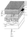
- Fig. 1 is a perspective view of a floating electrode type pixel according to an embodiment of the present invention.
- Fig. 2 is an equivalent circuit of the floating electrode type pixel.
- Fig. 3 (A) is a graph showing an applied voltage-transmissions characteristics of liquid crystal and Fig.3(B) is a graph showing photo-electric conversion characteristics in the embodiment.
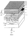
- Fig. 4 is a perspective view of a diffusion electrode-type pixel according to an embodiment of the present invention.
- Fig. 5 is an equivalent circuit of the diffusion electrode-type pixel.
- Fig. 6(A) is a perspective view of the structure of a pixel having an aperture formed by using transparent resin
- Fig. 6(B) is a perspective view of the structure of a pixel having a lower electrode aperture
- Fig. 6(C) is a perspective view of the structure of the pixel having an upper electrode aperture of the floating electrode type
- Fig. 6(D) is a perspective view of the structure of a pixel having an upper electrode aperture of the embodiment of the diffusion electrode type.
- Fig. 7 is a perspective view of the structure of the solid-state image pickup device in another embodiment.
- Fig. 1 shows a perspective view of a floating electrode-type pixel. Incident light is irradiated through a polarizing plate 101, a cover glass 102, a transparent electrode 103, an insulator 104, a liquid crystal 105, an insulator 106, a polarizing plate 107, an insulator 108, and a transparent electrode 109 to a photosite 113 constituted by N layer 114 and p-well 115 , and is converted to electron ,and then the signal charge is stored in a depletion layer capacitor formed at a junction part of the N layer 114 and the p-well 115.
- the photosite is separated from VCCD 117 by a channel stopper 116.
- a bias 118 is applied to a substrate and a bias 119 is applied to the liquid crystal 105.
- Poly-Si 110,111 are employed as electrodes of the VCCD 117.
- a depletion layer formed at a junction part of the N layer 114 and the p-well 115 corresponds to storing capacitor 204.
- a signal charge ⁇ Q sig generated by the incident light is stored in the storing capacitor of the depletion layer 204 and the capacitor of the insulator 202 as a signal charge quantity 203.
- the voltage V liq applied to the liquid crystal 105 by the bias 119 changes by a variation ⁇ V liq .
- ⁇ V liq ⁇ Q sig C liq C i +C i C PD +C PD C liq C i
- the voltage V liq applied to the liquid crystal 105 is reduced to (V liq - ⁇ V liq )205 by the photo generated signal charge .
- Fig.3 (A) shows the applied voltage - transmission characteristics of the liquid crystal 105.
- the transmission of the liquid crystal is the maximum value LC OFF 302 by the voltage V liq1 301 applied to the liquid crystal 105 .
- the voltage applied to the liquid crystal 105 varies to (V liq1 - ⁇ V liq )304 by the signal charge Q sig generated by incident light.
- the transmission of the liquid crystal 105 is reduced.
- the higher the incident light quantity is, the more the voltage applied to the liquid crystal 105 varies and the more the transmission of the liquid crystal 105 is reduced.
- the state corresponds to LC ON 306.
- Fig.3(B) shows the photo-electric conversion characteristics of the invented pixel having the transmission characteristics of Fig.3(A).
- the line 308 shows the invented one and the broken line 307 shows the conventional. Both photo-electric characteristics have the same saturation level.
- the more the incident light quantity increases , and the more the signal charge ⁇ Q sig increases the more the voltage applied to the liquid crystal 105 is reduced as shown in the equation (1), and the light transmission is reduced as shown in Fig.3(A).
- the saturation level 311 of the present invention pixel is shifted to a point of higher illumination side, thus revealing an expanded incident light range 312 as compared to the saturation level of the prior pixel.
- Shifting a knee point(bent point)313 of the photo-electric conversion characteristics line 308 to a point of lower illumination is realized by making the liquid crystal capacitance C liq 201 and the charging capacitance C PD 204 small, and/or making the insulator capacitance C i 202 large, because the shifting is realized by making the voltage ⁇ V liq modulated by the stored signal charge large in the equation (1).
- Fig. 4 show a perspective view of a diffusion electrode-type pixel element. Incident light is irradiated through a polarizing plate 401, a cover glass 402, a transparent electrode 403, an insulator 404, a liquid crystal 405, an insulator 406, a polarizing plate 407, an insulators 408, and a transparent electrode 409 to a photosite constituted by N layer 414 and p-well 415 , and is converted to electrons, and then the signal electrons are stored in a capacitor of a depletion layer formed in a junction part of the N layer 414 and the p-well 415.
- a bias 418 is applied to a substrate and a bias 419 is applied to the liquid crystal 405.
- Poly-Si 410,411 are employed as conversion electrode forming the VCCD 117.
- the transparent electrode 409 is connected to N layer 414.
- Fig. 5 shows a circuit equivalent to the diffusion electrode-type pixel.
- the capacitor in the depletion layer formed at the junction part of the N layer 414 and the p-well 415 for accumulating the signal charge as described above corresponds to a photosite capacitor 503.
- the signal charge Q sig generated by the incident light is stored in the storing capacitor 503 and the liquid crystal capacitor 501 as signal charge quantity 502.
- the voltage Viiq applied to the liquid crystal 405 by the bias 419 varies by ⁇ V liq .
- the variation ⁇ V liq of the voltage applied to the liquid crystal 405 can be expressed in the following equation (2) by using a liquid capacitance C liq 501 and an storing capacitance C PD 503.
- ⁇ V liq ⁇ Q sig C PD +C liq
- the upper limit of the incident light range is shifted to a point of higher illumination as compared to the prior CCD, as described in the photo-electric conversion characteristics line 308. Since the transparent electrode 409 is connected to N layer 414, more dynamic voltage modulation can be obtained.
- shifting a knee point(bent point)313 of the photo-electric conversion characteristics line 308 to a point of lower illumination is realized by making the liquid crystal capacitance C liq 501 and the photodiode capacitance C PD 503 small, because the shifting is realized by making the voltage ⁇ V liq modulated by the stored signal charge large in the equation (2).
- Fig. 6(A) shows a perspective view of the structure of a floating gate type improving MTF. Since the outside appearance of the structure is the same as that of Fig.1, Fig.6(A) shows such structure that the polarizing plate 101 and the cover glass 102 are removed from the structure of Fig.1.
- 603 is a transparent electrode
- 604 is an insulator
- 605 is a liquid crystal
- 606 is an insulator
- 607 is a polarizing plate
- 608 is an insulator
- 609 is a transparent electrode
- 614 is N layer
- 615 is a p-well
- 617 is VCCD
- 616 is a channel stopper.
- 618 is a bias and 619 is a bias and 610 and 611 are Poly-Si.
- a SiO 2 or a transparent resin 620 is formed boring through the liquid crystal 605 .
- the width of the transparent resin 620 is X-on 601 and the width of the photo-electric conversion area is X-off 602 which is larger than X-on 601.
- Fig.6(A) is a view in which the transparent electrode 603, the insulator 604 and the liquid crystal around the transparent resin 620 are removed for illustration convenience.
- the incident light quantity is large , the light transmission decreases and the aperture for the N layer 614 varies from X-off 602 to X-on 601.
- Fig. 6(B) shows a perspective view of the structure of a diffusion electrode type with improved MTF. Since the outside appearance of the structure is the same as that of Fig.4, in Fig.6(B) the polarizing plate 401 ,the cover glass 402, the transparent electrode 403 , the insulator 404 , the liquid crystal 405, the insulator 406, the polarizing plate 407 and the insulator 408 are not shown 623 is a lower transparent electrode , and 624 is an aperture of the lower transparent electrode 623 , and X- off 621 is the width of the aperture 624 and the X-on 622 is the width of the photo-electric conversion area ( the lower transparent electrode 623) .
- the structure of Fig.6(B) can improve MTF without using the transparent resin 620 of Fig.6(A), by using the lower transparent electrode 623 having the aperture 624.
- the part of the liquid crystal above the aperture 624 is not effected by the modulation voltage of the signal charge ⁇ Q sig , and the liquid crystal part becomes a state of LC OFF 302 and thereby the light transmission above the aperture 624 becomes constant irrespectively of the incident light quantity .
- the liquid crystal part between the transparent electrode 623 and the transparent electrode 103 is supplied with the modulation voltage of the signal charge ⁇ Q sig as shown by the equation (1).
- solid line 308 of the photo-electric conversion characteristics the saturation level 311 of the present invention pixel is shifted to a point of higher illumination, thus reveiling an expanded incident light range 312 as compared to the saturation level of the prior pixel.
- Fig.7 is an embodiment of the solid-state image pickup device applying the structure of the element unit of Fig.6(A), Fig6(B).
- 701 indicates p-layer
- 702 indicates n-layer
- 703 indicates 1st-Poly Silicon
- 704 indicates 2nd-Poly Silicon.
- 705(real line hatching ) shows such light shut state LC ON of the liquid crystal ON by strong incident light
- 706(chain line ) shows such light transparent state LC OFF of the liquid crystal OFF by non-strong incident light.
- liquid crystal ON realizes reduction of light transmission, and thereby the intensity level of the incident light can be fed back in same frame/field period and the element unit can be controlled individually.
- the upper transparent electrode 103 can be partly removed ,thereby forming an aperture and improving MTF.
- electrochromism and so on which have voltage-light transmission characteristics as shown in Fig. 3(A) can be used.
- the upper transparent electrode 103 can be partly removed in the embodiment of the diffusion electrode type ,thereby forming an aperture and improving MTF.
- MTF can be improved by partly restricting the liquid crystal 105 by using other method than the above mentioned using of the transparent resin (SiO 2 ) 620.
- glass material can be used.
- the aperture or transparent resin can be disposed anywhere within the area of the photo-electric conversion area to improve MTF.
- the luminous energy of the incident light can be corrected on a chip during the same frame/field in element unit , whereby the upper limit of the range of the luminous energy of the incident light may be shifted to a point of higher illumination. Then, a wide dynamic range can be obtained.
- an aperture window narrower in area than that of the photo-electric conversion part is provided , thereby allowing an element in which the MTF is improved when there is a large amount of the luminous energy of incident light.
Landscapes
- Physics & Mathematics (AREA)
- Nonlinear Science (AREA)
- Mathematical Physics (AREA)
- Chemical & Material Sciences (AREA)
- Crystallography & Structural Chemistry (AREA)
- General Physics & Mathematics (AREA)
- Optics & Photonics (AREA)
- Transforming Light Signals Into Electric Signals (AREA)
Claims (9)
- Dispositif de prise de vue à état solide comprenant :
des photosites (114, 115 ; 413, 414, 415) disposés sous forme de matrice sur un substrat, destinés à convertir la lumière incidente en photoélectrons et à stocker une charge de signal converti photoélectriquement et une couche de commande de lumière incidente (105 ; 405) disposées sur un côté incident de lumière de ces photosites,
caractérisé par des moyens (109, 409) pour moduler la transmission de lumière de la couche de commande de lumière incidente correspondant à la quantité de charge de signaux stockés. - Dispositif selon la revendication 1,
caractérisé en ce quela couche de commande de lumière incidente (105 ; 405) a une électrode transparente (109 ; 409) ;cette transmission de lumière incidente est modulée par la tension ; etla charge de signaux stockés affecte cette électrode transparente (109 ; 409) modulant ainsi la transmission de lumière incidente. - Dispositif selon la revendication 1,
caractérisé en ce quela couche de commande de lumière incidente (105 ; 405) a une première électrode transparente (103) disposée sur le côté incident de lumière de la couche de commande de lumière incidente et une seconde électrode transparente (109) disposée entre la couche de commande de lumière incidente et le photosite (113, 114, 115),la transmission de lumière incidente est modulée par la tension,la première électrode transparente (103) est alimentée en tension de polarisation et la seconde électrode transparente (109) est à l'état de flottement. - Dispositif selon la revendication 1,
caractérisé en ce quela couche de commande de lumière incidente (405) comporte une première électrode transparente (403) disposée sur le côté incident de lumière de la couche de commande de lumière incidente et une seconde électrode transparente (409) disposée sur le photosite (413, 414, 415),la transmission de lumière incidente est modulée par la tension,la première électrode transparente (403) est alimentée en tension de polarisation, etla seconde électrode transparente (409) est connectée à une partie de diffusion d'impuretés de déplétion du photosite (413, 414, 415). - Dispositif selon la revendication 1,
caractérisé en ce que
la surface d'une partie où est modulée cette transmission de lumière incidente est plus étroite qu'une surface de la section d'ouverture du photosite. - Dispositif selon la revendication 3 ou 4,
caractérisé en ce que
la première électrode transparente (103 ; 403) a une section d'ouverture plus étroite que la section d'ouverture du photosite (113 ; 114). - Dispositif selon la revendication 3 ou 4,
caractérisé en ce que
la seconde électrode transparente (109 ; 409) a une section d'ouverture plus étroite que la section d'ouverture du photosite. - Dispositif selon la revendication 1,
caractérisé en ce que
la couche de commande de lumière incidente est disposée à une section partielle au-dessus de la section d'ouverture du photosite. - Dispositif selon la revendication 8,
caractérisé en ce qu'
un élément transparent est disposé au niveau de l'autre section au-dessus de la section d'ouverture du photosite.
Applications Claiming Priority (2)
| Application Number | Priority Date | Filing Date | Title |
|---|---|---|---|
| JP10003991 | 1991-05-01 | ||
| JP100039/91 | 1991-05-01 |
Publications (3)
| Publication Number | Publication Date |
|---|---|
| EP0511644A2 EP0511644A2 (fr) | 1992-11-04 |
| EP0511644A3 EP0511644A3 (en) | 1993-07-14 |
| EP0511644B1 true EP0511644B1 (fr) | 1997-07-23 |
Family
ID=14263385
Family Applications (1)
| Application Number | Title | Priority Date | Filing Date |
|---|---|---|---|
| EP92107295A Expired - Lifetime EP0511644B1 (fr) | 1991-05-01 | 1992-04-29 | Dispositif état solide de prise de vues |
Country Status (3)
| Country | Link |
|---|---|
| US (1) | US5532743A (fr) |
| EP (1) | EP0511644B1 (fr) |
| DE (1) | DE69221018T2 (fr) |
Cited By (1)
| Publication number | Priority date | Publication date | Assignee | Title |
|---|---|---|---|---|
| EP2128740A1 (fr) * | 1998-08-31 | 2009-12-02 | Semiconductor Energy Laboratory Co, Ltd. | Dispositif d'affichage |
Families Citing this family (26)
| Publication number | Priority date | Publication date | Assignee | Title |
|---|---|---|---|---|
| JP3598648B2 (ja) * | 1996-04-02 | 2004-12-08 | ソニー株式会社 | 電荷転送素子及び電荷転送素子の駆動方法 |
| EP1122789A3 (fr) * | 2000-02-03 | 2004-01-07 | Agilent Technologies, Inc. (a Delaware corporation) | Capteur d'image utilisant du matériau photosensible pour l'augmentation de la plage dynamique et commande des capteurs d'image |
| CA2301345A1 (fr) * | 2000-03-17 | 2001-09-17 | Semiconductor Insights Inc. | Prise de cliche |
| US7023503B2 (en) * | 2002-02-20 | 2006-04-04 | Planar Systems, Inc. | Image sensor with photosensitive thin film transistors |
| US7009663B2 (en) | 2003-12-17 | 2006-03-07 | Planar Systems, Inc. | Integrated optical light sensitive active matrix liquid crystal display |
| US7053967B2 (en) | 2002-05-23 | 2006-05-30 | Planar Systems, Inc. | Light sensitive display |
| WO2003073159A1 (fr) | 2002-02-20 | 2003-09-04 | Planar Systems, Inc. | Ecran photosensible |
| US7372510B2 (en) * | 2002-03-01 | 2008-05-13 | Planar Systems, Inc. | Reflection resistant touch screens |
| US7219241B2 (en) * | 2002-11-30 | 2007-05-15 | Intel Corporation | Method for managing virtual and actual performance states of logical processors in a multithreaded processor using system management mode |
| JP2004233163A (ja) * | 2003-01-29 | 2004-08-19 | Hitachi High-Technologies Corp | パターン欠陥検査方法およびその装置 |
| US20080084374A1 (en) | 2003-02-20 | 2008-04-10 | Planar Systems, Inc. | Light sensitive display |
| US20050134749A1 (en) * | 2003-12-19 | 2005-06-23 | Adiel Abileah | Reflection resistant display |
| US7773139B2 (en) | 2004-04-16 | 2010-08-10 | Apple Inc. | Image sensor with photosensitive thin film transistors |
| US8054356B2 (en) * | 2007-02-14 | 2011-11-08 | Fujifilm Corporation | Image pickup apparatus having a charge storage section and charge sweeping section |
| US9310923B2 (en) | 2010-12-03 | 2016-04-12 | Apple Inc. | Input device for touch sensitive devices |
| US9329703B2 (en) | 2011-06-22 | 2016-05-03 | Apple Inc. | Intelligent stylus |
| US8638320B2 (en) | 2011-06-22 | 2014-01-28 | Apple Inc. | Stylus orientation detection |
| US8928635B2 (en) | 2011-06-22 | 2015-01-06 | Apple Inc. | Active stylus |
| US9557845B2 (en) | 2012-07-27 | 2017-01-31 | Apple Inc. | Input device for and method of communication with capacitive devices through frequency variation |
| US9652090B2 (en) | 2012-07-27 | 2017-05-16 | Apple Inc. | Device for digital communication through capacitive coupling |
| US9176604B2 (en) | 2012-07-27 | 2015-11-03 | Apple Inc. | Stylus device |
| US10048775B2 (en) | 2013-03-14 | 2018-08-14 | Apple Inc. | Stylus detection and demodulation |
| US10845901B2 (en) | 2013-07-31 | 2020-11-24 | Apple Inc. | Touch controller architecture |
| US10061449B2 (en) | 2014-12-04 | 2018-08-28 | Apple Inc. | Coarse scan and targeted active mode scan for touch and stylus |
| US10474277B2 (en) | 2016-05-31 | 2019-11-12 | Apple Inc. | Position-based stylus communication |
| CN109164624B (zh) * | 2018-09-30 | 2021-08-17 | 京东方科技集团股份有限公司 | 显示面板、显示装置及其图像获取方法 |
Family Cites Families (12)
| Publication number | Priority date | Publication date | Assignee | Title |
|---|---|---|---|---|
| JPS5685792A (en) * | 1979-12-14 | 1981-07-13 | Citizen Watch Co Ltd | Liquid crystal display unit |
| US4583002A (en) * | 1983-06-06 | 1986-04-15 | Fuji Photo Film Co., Ltd. | Imaging sensor with automatic sensitivity control comprising voltage multiplying means |
| US4838652A (en) * | 1985-05-15 | 1989-06-13 | Canon Kabushiki Kaisha | Image forming apparatus |
| US4767192A (en) * | 1986-10-31 | 1988-08-30 | International Business Machines Corporation | Light activated light valve with a silicon control element |
| JP2549650B2 (ja) * | 1987-03-31 | 1996-10-30 | 株式会社東芝 | 固体撮像装置 |
| US4807976A (en) * | 1987-04-01 | 1989-02-28 | Hughes Aircraft Company | Light valve system and method with pulsed readout |
| FR2626385B1 (fr) * | 1988-01-22 | 1991-10-11 | Thomson Csf | Obturateur selectif de lumiere, procede de realisation et son application a un detecteur d'image |
| GB8802025D0 (en) * | 1988-01-29 | 1988-02-24 | Minnesota Mining & Mfg | Imaging method & apparatus |
| NL8802082A (nl) * | 1988-08-23 | 1990-03-16 | Copyguard Enterprises | Videocamera met automatische sterkteregeling. |
| JPH0276481A (ja) * | 1988-08-26 | 1990-03-15 | Nec Eng Ltd | 撮像装置 |
| JPH02178612A (ja) * | 1988-12-28 | 1990-07-11 | Victor Co Of Japan Ltd | 光変調方法及び装置 |
| US5280359A (en) * | 1991-04-05 | 1994-01-18 | Matsushita Electric Industrial Co., Ltd. | Image pick-up device with auto lens control for freely selecting photometric area |
-
1992
- 1992-04-29 EP EP92107295A patent/EP0511644B1/fr not_active Expired - Lifetime
- 1992-04-29 DE DE69221018T patent/DE69221018T2/de not_active Expired - Fee Related
-
1994
- 1994-11-17 US US08/344,681 patent/US5532743A/en not_active Expired - Fee Related
Cited By (1)
| Publication number | Priority date | Publication date | Assignee | Title |
|---|---|---|---|---|
| EP2128740A1 (fr) * | 1998-08-31 | 2009-12-02 | Semiconductor Energy Laboratory Co, Ltd. | Dispositif d'affichage |
Also Published As
| Publication number | Publication date |
|---|---|
| DE69221018D1 (de) | 1997-08-28 |
| EP0511644A3 (en) | 1993-07-14 |
| DE69221018T2 (de) | 1998-01-22 |
| US5532743A (en) | 1996-07-02 |
| EP0511644A2 (fr) | 1992-11-04 |
Similar Documents
| Publication | Publication Date | Title |
|---|---|---|
| EP0511644B1 (fr) | Dispositif état solide de prise de vues | |
| US3953733A (en) | Method of operating imagers | |
| US6559889B2 (en) | Solid-state imaging apparatus with lowered overflow drain bias, method for driving same and camera using same | |
| DE4417159C2 (de) | CCD-Festkörperbildaufnehmer mit Überlaufdrainstruktur | |
| KR0183761B1 (ko) | 고체촬상소자 및 그 제조방법 | |
| EP0186162B1 (fr) | Capteur d'image à l'état solide | |
| US4891682A (en) | Solid state image pick-up device having a number of static induction transistor image sensors | |
| US6778214B1 (en) | Charge generation of solid state image pickup device | |
| US4845566A (en) | Solid-state image pickup apparatus having controllable means for eliminating surplus charge | |
| US6180935B1 (en) | Dynamic range extension of CCD imagers | |
| KR100255531B1 (ko) | 고체 촬상 장치 및 구동 방법 | |
| JPH04313268A (ja) | 固体撮像装置 | |
| US6778215B1 (en) | Driving method of solid-state image pickup device and image pickup system | |
| US6486460B1 (en) | Solid-state image sensing device and method of driving the same | |
| US5270558A (en) | Integrated electronic shutter for charge-coupled devices | |
| US4479139A (en) | Charge coupled device open circuit image detector | |
| JP3182204B2 (ja) | 固体撮像装置 | |
| US5528294A (en) | Method for eradicating smear in a charge-coupled device camera | |
| US5898460A (en) | Solid-state imaging device | |
| JPH02194779A (ja) | 撮像装置 | |
| KR20140069173A (ko) | 이미징 센서 | |
| EP0991128B1 (fr) | Augmentation de la plage dynamique de capteurs d'images à CCD | |
| EP0683602B1 (fr) | Procédé et appareillage pour un dispositif à couplage de charges à faible bruit | |
| KR100508610B1 (ko) | 고체촬상장치및그구동방법과카메라 | |
| EP0064081B1 (fr) | Detecteur d'image a circuit ouvert d'un dispositif de couplage de charge |
Legal Events
| Date | Code | Title | Description |
|---|---|---|---|
| PUAI | Public reference made under article 153(3) epc to a published international application that has entered the european phase |
Free format text: ORIGINAL CODE: 0009012 |
|
| AK | Designated contracting states |
Kind code of ref document: A2 Designated state(s): DE FR GB |
|
| PUAL | Search report despatched |
Free format text: ORIGINAL CODE: 0009013 |
|
| AK | Designated contracting states |
Kind code of ref document: A3 Designated state(s): DE FR GB |
|
| 17P | Request for examination filed |
Effective date: 19931229 |
|
| 17Q | First examination report despatched |
Effective date: 19950807 |
|
| GRAG | Despatch of communication of intention to grant |
Free format text: ORIGINAL CODE: EPIDOS AGRA |
|
| GRAH | Despatch of communication of intention to grant a patent |
Free format text: ORIGINAL CODE: EPIDOS IGRA |
|
| GRAH | Despatch of communication of intention to grant a patent |
Free format text: ORIGINAL CODE: EPIDOS IGRA |
|
| GRAA | (expected) grant |
Free format text: ORIGINAL CODE: 0009210 |
|
| AK | Designated contracting states |
Kind code of ref document: B1 Designated state(s): DE FR GB |
|
| REF | Corresponds to: |
Ref document number: 69221018 Country of ref document: DE Date of ref document: 19970828 |
|
| ET | Fr: translation filed | ||
| PLBE | No opposition filed within time limit |
Free format text: ORIGINAL CODE: 0009261 |
|
| STAA | Information on the status of an ep patent application or granted ep patent |
Free format text: STATUS: NO OPPOSITION FILED WITHIN TIME LIMIT |
|
| 26N | No opposition filed | ||
| REG | Reference to a national code |
Ref country code: GB Ref legal event code: IF02 |
|
| PGFP | Annual fee paid to national office [announced via postgrant information from national office to epo] |
Ref country code: GB Payment date: 20040428 Year of fee payment: 13 |
|
| PGFP | Annual fee paid to national office [announced via postgrant information from national office to epo] |
Ref country code: DE Payment date: 20040506 Year of fee payment: 13 |
|
| PGFP | Annual fee paid to national office [announced via postgrant information from national office to epo] |
Ref country code: FR Payment date: 20050408 Year of fee payment: 14 |
|
| PG25 | Lapsed in a contracting state [announced via postgrant information from national office to epo] |
Ref country code: GB Free format text: LAPSE BECAUSE OF NON-PAYMENT OF DUE FEES Effective date: 20050429 |
|
| PG25 | Lapsed in a contracting state [announced via postgrant information from national office to epo] |
Ref country code: DE Free format text: LAPSE BECAUSE OF NON-PAYMENT OF DUE FEES Effective date: 20051101 |
|
| GBPC | Gb: european patent ceased through non-payment of renewal fee |
Effective date: 20050429 |
|
| REG | Reference to a national code |
Ref country code: FR Ref legal event code: ST Effective date: 20061230 |
|
| PG25 | Lapsed in a contracting state [announced via postgrant information from national office to epo] |
Ref country code: FR Free format text: LAPSE BECAUSE OF NON-PAYMENT OF DUE FEES Effective date: 20060502 |