EP0508872B1 - System zur optischen Belichtung für einen Videofarbdrucker - Google Patents
System zur optischen Belichtung für einen Videofarbdrucker Download PDFInfo
- Publication number
- EP0508872B1 EP0508872B1 EP92400952A EP92400952A EP0508872B1 EP 0508872 B1 EP0508872 B1 EP 0508872B1 EP 92400952 A EP92400952 A EP 92400952A EP 92400952 A EP92400952 A EP 92400952A EP 0508872 B1 EP0508872 B1 EP 0508872B1
- Authority
- EP
- European Patent Office
- Prior art keywords
- color
- liquid crystal
- optical exposure
- exposure system
- lines
- Prior art date
- Legal status (The legal status is an assumption and is not a legal conclusion. Google has not performed a legal analysis and makes no representation as to the accuracy of the status listed.)
- Expired - Lifetime
Links
- 230000003287 optical effect Effects 0.000 title claims description 52
- 239000004973 liquid crystal related substance Substances 0.000 claims description 62
- 238000004519 manufacturing process Methods 0.000 description 7
- 239000000835 fiber Substances 0.000 description 6
- 238000000034 method Methods 0.000 description 6
- 239000003086 colorant Substances 0.000 description 4
- 239000010409 thin film Substances 0.000 description 4
- 238000010276 construction Methods 0.000 description 3
- BQCADISMDOOEFD-UHFFFAOYSA-N Silver Chemical compound [Ag] BQCADISMDOOEFD-UHFFFAOYSA-N 0.000 description 1
- 230000002950 deficient Effects 0.000 description 1
- 230000001419 dependent effect Effects 0.000 description 1
- 238000010586 diagram Methods 0.000 description 1
- 239000010408 film Substances 0.000 description 1
- 230000001678 irradiating effect Effects 0.000 description 1
- 229910052709 silver Inorganic materials 0.000 description 1
- 239000004332 silver Substances 0.000 description 1
Images

Classifications
-
- B—PERFORMING OPERATIONS; TRANSPORTING
- B41—PRINTING; LINING MACHINES; TYPEWRITERS; STAMPS
- B41J—TYPEWRITERS; SELECTIVE PRINTING MECHANISMS, i.e. MECHANISMS PRINTING OTHERWISE THAN FROM A FORME; CORRECTION OF TYPOGRAPHICAL ERRORS
- B41J2/00—Typewriters or selective printing mechanisms characterised by the printing or marking process for which they are designed
- B41J2/435—Typewriters or selective printing mechanisms characterised by the printing or marking process for which they are designed characterised by selective application of radiation to a printing material or impression-transfer material
-
- H—ELECTRICITY
- H04—ELECTRIC COMMUNICATION TECHNIQUE
- H04N—PICTORIAL COMMUNICATION, e.g. TELEVISION
- H04N1/00—Scanning, transmission or reproduction of documents or the like, e.g. facsimile transmission; Details thereof
- H04N1/46—Colour picture communication systems
- H04N1/50—Picture reproducers
-
- H—ELECTRICITY
- H04—ELECTRIC COMMUNICATION TECHNIQUE
- H04N—PICTORIAL COMMUNICATION, e.g. TELEVISION
- H04N1/00—Scanning, transmission or reproduction of documents or the like, e.g. facsimile transmission; Details thereof
- H04N1/024—Details of scanning heads ; Means for illuminating the original
- H04N1/032—Details of scanning heads ; Means for illuminating the original for picture information reproduction
- H04N1/036—Details of scanning heads ; Means for illuminating the original for picture information reproduction for optical reproduction
-
- H—ELECTRICITY
- H04—ELECTRIC COMMUNICATION TECHNIQUE
- H04N—PICTORIAL COMMUNICATION, e.g. TELEVISION
- H04N1/00—Scanning, transmission or reproduction of documents or the like, e.g. facsimile transmission; Details thereof
- H04N1/40—Picture signal circuits
- H04N1/40025—Circuits exciting or modulating particular heads for reproducing continuous tone value scales
Definitions
- the present invention relates in general to a color video printer, and more particularly to an optical exposure system for such a color video printer which uses conventional inexpensive liquid crystal elements of 8-gradation transmittivities, increases number of color gradations, thus improves the image quality.
- color video printers are generally provided with optical exposure system for recording or printing an image on a photosensitive medium by producing an optical image for an electric image signal and exposing the photosensitive medium to a light of the optical image.
- optical exposure system for producing the optical image for the electric image signal.
- FOLCD fiber optics liquid crystal display
- the known FOLCD package generally comprises a liquid crystal display (LCD) panel for producing the optical image for the electric image signal synchronously with a scanning signal.
- LCD liquid crystal display
- a back light source for irradiating a light to the LCD panel part in order to make the photosensitive medium to be exposed to the optical image which has been produced by the LCD panel
- a fiber optics face plate having a screen for making the photosensitive medium to be exposed to the optical image of the LCD panel.
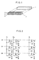
- the LCD panel of the known optical exposure system generally comprises a LCD part 1 for producing the optical image for the electric image signal by red(R), green(G) and blue(B) color lines and a color filter part 2 which adheres to the LCD part 1 in order to bring out the R, G and B colors.
- the equivalent circuit of the LCD part 1 is constructed by the R, G and B color lines such that three groups of liquid crystal elements (L R1 - L Rh ), (L G1 - L Gh )and (L B1 - L Bh ) are arranged corresponding to the R, G and B lines, each common electrode terminal of the above liquid crystal elements (L R1 - L Rh ) , (L G1 - L Gh ) and (L B1 - L Bh ) is grounded, and the signal electrode terminals of the liquid crystal elements (L R1 - L Rh ), (L G1 - L Gh ) and (L B1 - L Bh ) are connected to the source terminals of three groups of thin film transistors (T R1 - T Rh ), (T G1 - T Gh ) and (T B1 - T Bh ), respectively.
- T R1 - T Rh thin film transistors
- the gates of the thin film transistors (T R1 -T Rh ), (T G1 - T Gh ) and (T B1 - T Bh ) are connected to the R, G and B gate lines G R , G G , and G B by the R, G and B lines, respectively.
- the drain terminals of the thin film transistors (T R1 , T G1 and T B1 ) , (T R2 , T G2 and T B2 ) , ---- (T Rh , T Gh and T Bh ) are connected, by pixels, to the drain lines D 1 , D 2 , ----D h , respectively.
- the color filter part 2 comprises R, G and B color filters corresponding to the three groups of liquid crystal elements (L R1 - L Rh ), (L G1 - L Gh ) and (L B1 - L Bh ), respectively.
- the horizontal scanning signals are applied to the R, G and B gate lines G R , G G , and G B at predetermined periods and then the signal voltages corresponding to the pixels are sequentially applied to the drain lines D 1 , D 2 ,----,D h synchronously with the horizontal scanning signals applied to the R, G and B gate lines, the thin film transistors (T R1 , T G1 and T B1 ), (T R2 , T G2 and T B2 ), ---- (T Rh , T Gh and T Bh ) are turned on, thereby applying the signal voltages corresponding to the pixels to the liquid crystal elements (L R1 - L Rh ), (L G1 - L Gh ) and (L B1 - L Bh ), respectively.
- the liquid crystal elements (L R1 - L Rh ), (L G1 - L Gh ) and (L B1 - L Bh ) maintain the respective signal voltages, having been applied thereto, for one period by means of a condenser. Therefore, the transmittivities of the liquid crystal elements (L R1 - L Rh ), (L G1 - L Gh ) and (L B1 - L Bh ) are varied in proportion to the signal voltages applied thereto.
- the back light source irradiates the light to the LCD panel.
- the LCD panel makes the quantity of light which is transmitted therethrough to be varied in proportion to the signal voltages due to the respective transmittivities of the liquid crystal elements (L R1 - L Rh ), (L G1 - L Gh ) and (L B1 - L Bh ).
- the transmitted light is then applied to the color filter part 2 in order to cause the R, G and B colors to be brought out thereby.
- the R, G and B color lights from the color filter part 2 are transmitted through the fiber optics face plate, thereby causing the photosensitive medium to be exposed thereto.
- the photosensitive medium is exposed to the optical color image at the optical exposure system, then heated itself by a heat fixing system in order to fix the color image thereof.
- the photosensitive medium is exposed to the optical color image at the optical exposure system, then compressed with a receiver paper by a developing system in order to develop the color image thereof onto a receiver paper which is then heated by the heat fixing system in order to fix the color image thereof.
- the number of color gradations of the printed image is substantially influenced by the number of gradations of transmittivities of the liquid crystal elements.
- the number of gradations of transmittivities of the liquid crystal elements gradually increase as technique for manufacturing the liquid crystal element advances.
- the increase of the number of gradations of transmittivities of the liquid crystal elements is obliged to be limited in view of the present technical level.
- the higher the number of gradations of transmittivities increases the more the manufacturing process of the liquid crystal element is accompanied with difficulty, thereby causing the manufacturing cost to substantially increase.
- the liquid crystal elements of 8-gradation transmittivities are appropriate in view of the present level of technique for manufacturing the liquid crystal element, thus they are wide used.
- the known optical exposure system for the color video printer generally comprises the liquid crystal elements of 8-gradation transmittivities, thus the transmittivity of the color filter part is obliged to be fixed at a predetermined level.
- the known optical exposure system for color video printer provided with the conventional liquid crystal elements of 8-gradation transmittivities can vary the transmittivities of the liquid crystal elements by 8 gradations for each color R, G, B.
- the number of gradations resulting from the variance of the transmittivities of the liquid crystal elements of this system is substantially deficient in providing the desired natural color, thereby causing the printer to provide a bad image quality.
- the optical exposure system may be provided with the liquid crystal elements of increased number of gradations of transmittivities, but this type of optical exposure system has a disadvantage of a difficult manufacturing process and also expensive manufacturing cost.
- Document DE-A-4 106 016 discloses a device for producing an image for a video printer comprising a LCD part with lines of red, green and blue pixels, in accordance with the preamble of claim 1.
- the above-mentioned object of the present invention can be accomplished by providing an optical exposure system for a color video printer according to claim 1.
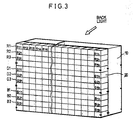
- the LCD panel includes a LCD part 10 comprising, in each red(R), green(G) and blue(B) line, a plurality of liquid crystal element lines, respectively.
- the LCD panel is additionally provided with a color filter part 20 comprising, in the red(R), green(G) and blue(B) lines, a plurality of color filters (R1, R2, --), (G1, G2, --), and (B1, B2, --) corresponding to the R, G and B lines of the LCD part 10, respectively.
- the LCD elements of the LCD part 10 are conventional LCD elements of 8-gradation transmittivities and the color filter part 20 is constructed of color filters having different transmittivities in the lines of each color R, G, B.
- the color filter part 20 is constructed such that the transmittivity ratio thereof in the R, G and B lines can be described as follows: 1/K 0 : 1/K 1 : ------ : 1/K n-1
- K is the number of gradations of each liquid crystal element.
- each liquid crystal element is a liquid crystal element of 8 gradations
- the number K of gradations of the liquid crystal element will be "8".
- this optical exposure system is provided with the multi-flow type LCD panel which includes the LCD part 10 comprising, by the red(R), green(G) and blue(B) lines, the plurality of liquid crystal element lines, respectively, and the color filter part 20 comprising, by the red(R), green(G) and blue(B) lines, the plurality of color filters (R1, R2, --), (G1, G2, --), and (B1, B2, --) corresponding to the R, G and B lines of the LCD part 10, respectively.
- the liquid crystal elements of the LCD part 10 comprise conventional liquid crystal elements of 8- gradation transmittivities and the color filter part 20 is constructed of the color filters having the different transmittivities by the lines of each color R, G, B.
- the optical exposure system having the multi-flow type LCD panel makes one horizontal line of a photosensitive medium to be exposed to the R, G and B color lights by several times for each color light, respectively, thereby reducing the required time for the optical exposure process and thus accomplishing a high speed printing.
- the optical exposure system of this invention including the color filter part 20 comprising the color filters having the different transmittivities by the lines makes one horizontal line of a photosensitive medium to be repeatedly exposed to the R, G and B color lights, respectively.
- the value resulting from multiplying the gradation data by the gain in consideration of the transmittivity of each corresponding color filter is applied to an equivalent circuit of the LCD panel as a liquid crystal driving signal value.
- this optical exposure system when this optical exposure system repeatedly exposes the one horizontal line of the photosensitive medium to the R, G and B color lights several times for each color light, it increases the number of color gradations by virtue of the different transmittivities of the color filters for each color light R, G, B.
- the transmittivity ratio of the color filters will be 1 : 1/8 : 1/64.
- the number of color gradations will be X 1 /8 + X 2 /64 + X 3 /512, that is, the number of (64X 1 + 8X 2 + X 3 )/512.
- each liquid crystal element has a transmittivity of a predetermined number of gradations, for example, 8 gradations
- the data value for R color expression of the subject pixel is X and also the eight-step fixing value of the data value X is X x
- the quantity of optical exposure light in case of the optical exposure by using the liquid crystal element of 8 gradations, that is, the quantity of light transmitted through the liquid crystal element will be a value of X X /8.
- the method for calculating the eight-step fixing values X 1 , X 2 and X 3 for example, in case of assuming that the data value of R color light exposure for the subject pixel of an optical exposure system of 512-gradation expression is "363", can be described as follows.
- the first fixing value X 1 is selected as "5".
- the value resulting from multiplying "64” by "5" is "320”
- the value "320” is subtracted from the data value "363” in order to obtain the result value "43”.
- the second fixing value X 2 is selected as "5".
- the number of gradations "8" is multiplied by "5" in order to obtain a result value "40” which is then subtracted from the value "43", thereby obtaining a result value "3”.
- the third fixing value X 3 is selected as "3".
- the liquid crystal element corresponding to the subject pixel and being disposed at the first R line is driven by a value of 5/8 in order to obtain a quantity of optical exposure light of 320/512.
- the liquid crystal element corresponding to the subject pixel and being disposed at the second R line is driven by a value of 5/8 in order to obtain a quantity of optical exposure light of 43/512.
- the liquid crystal element corresponding to the subject pixel disposed at the third R line is driven by a value of 3/8 in order to obtain a quantity of optical exposure light of 3/512.
- the subject pixel of the three LCD lines are driven by the values 5/8, 5/8 and 3/8, respectively.
- the color filters R1, R2 and R3 have the different transmittivities, the quantity of optical exposure light is totally 363/512.
- Figs. 4A to 4C illustrate the operation of the multi-flow type liquid crystal display panel of this invention, respectively.
- the transmittivities of the liquid crystal elements are determined in accordance with the magnitude of the values X 1 , X 2 and X 3 .
- the photosensitive medium 30 is normally fed under the condition of contacting with the optical exposure system.
- the liquid crystal elements are driven by the value X 1 in order to provide the predetermined quantity of optical exposure light 64*X 1 .
- the liquid crystal elements are driven by the value X 2 in order to provide the predetermined quantity of optical exposure light 8*X 2 .
- the liquid crystal elements are driven by the value X 1 in order to provide the predetermined quantity of optical exposure light 1*X 3 .
- the present invention provides a multi-flow type optical exposure system comprising a fiber optics liquid crystal package including a multi-flow type LCD panel which uses conventional liquid crystal elements of 8 gradations, is provided with color filters having the different transmittivities, thereby providing a gradation expression exceeding at least 64 gradations.
- the present invention provides advantage in that it improves the image quality of the printed image due to increase of the color gradations and also reduces the manufacturing cost of the color video printer due to use of conventional inexpensive liquid crystal elements of 8 gradations.
Landscapes
- Engineering & Computer Science (AREA)
- Multimedia (AREA)
- Signal Processing (AREA)
- Liquid Crystal (AREA)
- Printers Or Recording Devices Using Electromagnetic And Radiation Means (AREA)
- Fax Reproducing Arrangements (AREA)
- Optical Filters (AREA)
- Color, Gradation (AREA)
Claims (2)
- System zur optischen Belichtung für einen Videofarbdrucker, enthaltend eine Flüssigkristall-Anzeigeeinheit (10) mit roten (R), grünen (G) und blauen (B) Farblinien, dadurch gekennzeichnet, daß
jede der roten (R), grünen (G) und blauen (B) Farblinien eine Vielzahl von Flüssigkristallelementlinien aufweist und daß das System zur optischen Belichtung weiterhin eine Farbfiltereinheit (20) enthält, die für jede der roten (R), grünen (G) und blauen (B) Farblinien eine Vielzahl von Farbfiltern jeweils fur jede der Flüssigkristallelementlinien umfaßt, wobei die vielen Farbfilter für einige Farblinien verschiedene, vorherbestimmte Transmittivitäten besitzen, die eine Funktion der Anzahl der Übertragungsraten jeder Flüssigkristallelementlinie und der Anzahl der Farbfilter pro Farbe sind. - System zu optischen Belichtung gemäß Anspruch 1, gekennzeichnet dadurch, daß die vorherbestimmten Transmittivitäten der Vielzahl von Filtern durch das verhältniß 1/K0; 1/K1; ... ; 1/Kn-1 bestimmt werden, wobei K der Anzahl der Übertragungsraten jedes Flüssigkristallelements und n der Anzahl der Farbfilter pro Farbe entspricht.
Applications Claiming Priority (2)
| Application Number | Priority Date | Filing Date | Title |
|---|---|---|---|
| KR1019910005542A KR940009449B1 (ko) | 1991-04-06 | 1991-04-06 | 칼라비디오 프린터의 노광장치 |
| KR554291 | 1991-04-06 |
Publications (3)
| Publication Number | Publication Date |
|---|---|
| EP0508872A2 EP0508872A2 (de) | 1992-10-14 |
| EP0508872A3 EP0508872A3 (en) | 1993-02-10 |
| EP0508872B1 true EP0508872B1 (de) | 1996-09-25 |
Family
ID=19312987
Family Applications (1)
| Application Number | Title | Priority Date | Filing Date |
|---|---|---|---|
| EP92400952A Expired - Lifetime EP0508872B1 (de) | 1991-04-06 | 1992-04-06 | System zur optischen Belichtung für einen Videofarbdrucker |
Country Status (5)
| Country | Link |
|---|---|
| US (1) | US5493428A (de) |
| EP (1) | EP0508872B1 (de) |
| JP (1) | JPH06197369A (de) |
| KR (1) | KR940009449B1 (de) |
| DE (1) | DE69213989T2 (de) |
Families Citing this family (5)
| Publication number | Priority date | Publication date | Assignee | Title |
|---|---|---|---|---|
| US5844663A (en) * | 1996-09-13 | 1998-12-01 | Electronic Systems Engineering Co. | Method and apparatus for sequential exposure printing of ultra high resolution digital images using multiple multiple sub-image generation and a programmable moving-matrix light valve |
| US5946031A (en) * | 1996-10-22 | 1999-08-31 | Polaroid Corporation | Electronic still camera with printing capability |
| US6078303A (en) | 1996-12-19 | 2000-06-20 | Colorado Microdisplay, Inc. | Display system having electrode modulation to alter a state of an electro-optic layer |
| US6046716A (en) | 1996-12-19 | 2000-04-04 | Colorado Microdisplay, Inc. | Display system having electrode modulation to alter a state of an electro-optic layer |
| US5920298A (en) | 1996-12-19 | 1999-07-06 | Colorado Microdisplay, Inc. | Display system having common electrode modulation |
Family Cites Families (13)
| Publication number | Priority date | Publication date | Assignee | Title |
|---|---|---|---|---|
| IL60156A (en) * | 1980-05-25 | 1984-11-30 | Stolov Michael | Large electronically controlled liquid crystal display of one or more colors |
| JPS63109069A (ja) * | 1986-10-27 | 1988-05-13 | Canon Inc | 液晶プリンタ装置 |
| JPH0268520A (ja) * | 1988-09-02 | 1990-03-08 | Sharp Corp | 表示装置 |
| FR2637407B1 (fr) * | 1988-09-30 | 1994-02-11 | Commissariat A Energie Atomique | Procede d'affichage de niveaux de gris sur un ecran a cristaux liquides ferroelectriques a phase smectique chirale |
| JPH02166419A (ja) * | 1988-12-21 | 1990-06-27 | Nippon I B M Kk | 液晶表示装置 |
| JPH02227268A (ja) * | 1989-02-28 | 1990-09-10 | Sony Corp | プリンタ装置 |
| DE3910418A1 (de) * | 1989-03-31 | 1990-10-04 | Licentia Gmbh | Anzeigevorrichtung |
| US5216414A (en) * | 1989-11-20 | 1993-06-01 | Sharp Kabushiki Kaisha | Color liquid crystal display device |
| KR910016199A (ko) * | 1990-02-27 | 1991-09-30 | 이헌조 | 비데오 프린터의 결상장치 |
| NL9002011A (nl) * | 1990-09-13 | 1992-04-01 | Philips Nv | Weergeefinrichting. |
| DE4139407C2 (de) * | 1990-11-29 | 1993-11-11 | Gold Star Co | Vorrichtung und Verfahren zum Erzeugen von Bilddarstellungen in einem Farbvideodrucker |
| JP3029489B2 (ja) * | 1991-07-25 | 2000-04-04 | キヤノン株式会社 | 表示装置 |
| US5319480A (en) * | 1993-03-19 | 1994-06-07 | Honeywell Inc. | Liquid crystal half-tone display with gray level uniformity |
-
1991
- 1991-04-06 KR KR1019910005542A patent/KR940009449B1/ko not_active Expired - Fee Related
-
1992
- 1992-04-06 JP JP4084187A patent/JPH06197369A/ja active Pending
- 1992-04-06 US US07/863,824 patent/US5493428A/en not_active Expired - Lifetime
- 1992-04-06 EP EP92400952A patent/EP0508872B1/de not_active Expired - Lifetime
- 1992-04-06 DE DE69213989T patent/DE69213989T2/de not_active Expired - Fee Related
Also Published As
| Publication number | Publication date |
|---|---|
| KR940009449B1 (ko) | 1994-10-13 |
| KR920019537A (ko) | 1992-11-19 |
| JPH06197369A (ja) | 1994-07-15 |
| EP0508872A3 (en) | 1993-02-10 |
| US5493428A (en) | 1996-02-20 |
| EP0508872A2 (de) | 1992-10-14 |
| DE69213989T2 (de) | 1997-06-05 |
| DE69213989D1 (de) | 1996-10-31 |
Similar Documents
| Publication | Publication Date | Title |
|---|---|---|
| US4239385A (en) | Photographic copying machine with means for varying exposure across the surface of the original copied | |
| US4373156A (en) | Apparatus and method for producing rapid, high resolution hard color copies from computer-based graphics and digital image processing systems | |
| DE3642821A1 (de) | Farbnegativpruefgeraet | |
| DE3933150A1 (de) | Videodrucker | |
| DE3901516C2 (de) | Bildleseeinrichtung | |
| US4743963A (en) | Apparatus for magnifying or reducing a color image in which sequentially-stored RGB data are selectively read out from a memory in accordance with previously-determined read control data | |
| US5050001A (en) | Printing system with liquid crystal shutter matrix panel | |
| JPH10221783A (ja) | 画像形成ディスプレイを用いて感光材料上にプリントするための方法および装置 | |
| US4958237A (en) | Method of making enlarged prints by subdividing an original image and interpolating the subdivided image | |
| DE69127891T2 (de) | Digitale hartcopy-farbphotoreproduktionen mit internegativ | |
| EP0508872A2 (de) | System zur optischen Belichtung für einen Videofarbdrucker | |
| US4924302A (en) | CRT color video printer which eliminates magnification changes due to chromatic aberrations | |
| US5223960A (en) | Image-producing apparatus for a video printer | |
| KR920005770B1 (ko) | 인쇄복제용 원판필름 제작을 위한 장치 | |
| JPH08227108A (ja) | 液晶画像形成方法及び液晶画像形成装置 | |
| US5757410A (en) | Image-wise exposure apparatus and image displaying apparatus | |
| US5440399A (en) | Method for optical exposure in a color video printed utilizing LCD | |
| JPH08211844A (ja) | 画像表示方法 | |
| JPS6428623A (en) | Image forming device and its driving method | |
| DE60031600T2 (de) | Digitaler fotografischer Belichter mit subtraktiver Lichtmodulatoren-Zeile | |
| EP0512924A2 (de) | Optisches Belichtungssystem für Farbvideodrucker | |
| JP2545286B2 (ja) | 液晶シャッターマトリクスパネルを用いたプリンティング装置 | |
| JP2748944B2 (ja) | ビデオプリンタ | |
| JPS6053935A (ja) | 画像形成方法 | |
| DE4139407A1 (de) | Vorrichtung und verfahren zum erzeugen von bilddarstellungen in einem farbvideodrucker |
Legal Events
| Date | Code | Title | Description |
|---|---|---|---|
| PUAI | Public reference made under article 153(3) epc to a published international application that has entered the european phase |
Free format text: ORIGINAL CODE: 0009012 |
|
| AK | Designated contracting states |
Kind code of ref document: A2 Designated state(s): DE FR GB NL |
|
| PUAL | Search report despatched |
Free format text: ORIGINAL CODE: 0009013 |
|
| AK | Designated contracting states |
Kind code of ref document: A3 Designated state(s): DE FR GB NL |
|
| 17P | Request for examination filed |
Effective date: 19930508 |
|
| 17Q | First examination report despatched |
Effective date: 19950406 |
|
| RAP1 | Party data changed (applicant data changed or rights of an application transferred) |
Owner name: LG ELECTRONICS INC. |
|
| GRAH | Despatch of communication of intention to grant a patent |
Free format text: ORIGINAL CODE: EPIDOS IGRA |
|
| GRAH | Despatch of communication of intention to grant a patent |
Free format text: ORIGINAL CODE: EPIDOS IGRA |
|
| GRAA | (expected) grant |
Free format text: ORIGINAL CODE: 0009210 |
|
| AK | Designated contracting states |
Kind code of ref document: B1 Designated state(s): DE FR GB NL |
|
| PG25 | Lapsed in a contracting state [announced via postgrant information from national office to epo] |
Ref country code: NL Free format text: LAPSE BECAUSE OF FAILURE TO SUBMIT A TRANSLATION OF THE DESCRIPTION OR TO PAY THE FEE WITHIN THE PRESCRIBED TIME-LIMIT Effective date: 19960925 Ref country code: FR Effective date: 19960925 |
|
| REF | Corresponds to: |
Ref document number: 69213989 Country of ref document: DE Date of ref document: 19961031 |
|
| EN | Fr: translation not filed | ||
| NLV1 | Nl: lapsed or annulled due to failure to fulfill the requirements of art. 29p and 29m of the patents act | ||
| PLBE | No opposition filed within time limit |
Free format text: ORIGINAL CODE: 0009261 |
|
| STAA | Information on the status of an ep patent application or granted ep patent |
Free format text: STATUS: NO OPPOSITION FILED WITHIN TIME LIMIT |
|
| 26N | No opposition filed | ||
| PGFP | Annual fee paid to national office [announced via postgrant information from national office to epo] |
Ref country code: GB Payment date: 19980330 Year of fee payment: 7 |
|
| PGFP | Annual fee paid to national office [announced via postgrant information from national office to epo] |
Ref country code: DE Payment date: 19980414 Year of fee payment: 7 |
|
| PG25 | Lapsed in a contracting state [announced via postgrant information from national office to epo] |
Ref country code: GB Free format text: LAPSE BECAUSE OF NON-PAYMENT OF DUE FEES Effective date: 19990406 |
|
| GBPC | Gb: european patent ceased through non-payment of renewal fee |
Effective date: 19990406 |
|
| PG25 | Lapsed in a contracting state [announced via postgrant information from national office to epo] |
Ref country code: DE Free format text: LAPSE BECAUSE OF NON-PAYMENT OF DUE FEES Effective date: 20000201 |