EP0508628B1 - Method for driving active matrix type liquid crystal display device - Google Patents
Method for driving active matrix type liquid crystal display device Download PDFInfo
- Publication number
- EP0508628B1 EP0508628B1 EP92302419A EP92302419A EP0508628B1 EP 0508628 B1 EP0508628 B1 EP 0508628B1 EP 92302419 A EP92302419 A EP 92302419A EP 92302419 A EP92302419 A EP 92302419A EP 0508628 B1 EP0508628 B1 EP 0508628B1
- Authority
- EP
- European Patent Office
- Prior art keywords
- liquid crystal
- signal
- period
- voltage
- selection
- Prior art date
- Legal status (The legal status is an assumption and is not a legal conclusion. Google has not performed a legal analysis and makes no representation as to the accuracy of the status listed.)
- Expired - Lifetime
Links
Images












Classifications
-
- G—PHYSICS
- G09—EDUCATION; CRYPTOGRAPHY; DISPLAY; ADVERTISING; SEALS
- G09G—ARRANGEMENTS OR CIRCUITS FOR CONTROL OF INDICATING DEVICES USING STATIC MEANS TO PRESENT VARIABLE INFORMATION
- G09G3/00—Control arrangements or circuits, of interest only in connection with visual indicators other than cathode-ray tubes
- G09G3/20—Control arrangements or circuits, of interest only in connection with visual indicators other than cathode-ray tubes for presentation of an assembly of a number of characters, e.g. a page, by composing the assembly by combination of individual elements arranged in a matrix no fixed position being assigned to or needed to be assigned to the individual characters or partial characters
- G09G3/34—Control arrangements or circuits, of interest only in connection with visual indicators other than cathode-ray tubes for presentation of an assembly of a number of characters, e.g. a page, by composing the assembly by combination of individual elements arranged in a matrix no fixed position being assigned to or needed to be assigned to the individual characters or partial characters by control of light from an independent source
- G09G3/36—Control arrangements or circuits, of interest only in connection with visual indicators other than cathode-ray tubes for presentation of an assembly of a number of characters, e.g. a page, by composing the assembly by combination of individual elements arranged in a matrix no fixed position being assigned to or needed to be assigned to the individual characters or partial characters by control of light from an independent source using liquid crystals
- G09G3/3611—Control of matrices with row and column drivers
- G09G3/367—Control of matrices with row and column drivers with a nonlinear element in series with the liquid crystal cell, e.g. a diode, or M.I.M. element
-
- G—PHYSICS
- G09—EDUCATION; CRYPTOGRAPHY; DISPLAY; ADVERTISING; SEALS
- G09G—ARRANGEMENTS OR CIRCUITS FOR CONTROL OF INDICATING DEVICES USING STATIC MEANS TO PRESENT VARIABLE INFORMATION
- G09G3/00—Control arrangements or circuits, of interest only in connection with visual indicators other than cathode-ray tubes
- G09G3/20—Control arrangements or circuits, of interest only in connection with visual indicators other than cathode-ray tubes for presentation of an assembly of a number of characters, e.g. a page, by composing the assembly by combination of individual elements arranged in a matrix no fixed position being assigned to or needed to be assigned to the individual characters or partial characters
- G09G3/34—Control arrangements or circuits, of interest only in connection with visual indicators other than cathode-ray tubes for presentation of an assembly of a number of characters, e.g. a page, by composing the assembly by combination of individual elements arranged in a matrix no fixed position being assigned to or needed to be assigned to the individual characters or partial characters by control of light from an independent source
- G09G3/36—Control arrangements or circuits, of interest only in connection with visual indicators other than cathode-ray tubes for presentation of an assembly of a number of characters, e.g. a page, by composing the assembly by combination of individual elements arranged in a matrix no fixed position being assigned to or needed to be assigned to the individual characters or partial characters by control of light from an independent source using liquid crystals
- G09G3/3611—Control of matrices with row and column drivers
- G09G3/3674—Details of drivers for scan electrodes
-
- G—PHYSICS
- G09—EDUCATION; CRYPTOGRAPHY; DISPLAY; ADVERTISING; SEALS
- G09G—ARRANGEMENTS OR CIRCUITS FOR CONTROL OF INDICATING DEVICES USING STATIC MEANS TO PRESENT VARIABLE INFORMATION
- G09G2310/00—Command of the display device
- G09G2310/06—Details of flat display driving waveforms
-
- G—PHYSICS
- G09—EDUCATION; CRYPTOGRAPHY; DISPLAY; ADVERTISING; SEALS
- G09G—ARRANGEMENTS OR CIRCUITS FOR CONTROL OF INDICATING DEVICES USING STATIC MEANS TO PRESENT VARIABLE INFORMATION
- G09G2310/00—Command of the display device
- G09G2310/06—Details of flat display driving waveforms
- G09G2310/061—Details of flat display driving waveforms for resetting or blanking
-
- G—PHYSICS
- G09—EDUCATION; CRYPTOGRAPHY; DISPLAY; ADVERTISING; SEALS
- G09G—ARRANGEMENTS OR CIRCUITS FOR CONTROL OF INDICATING DEVICES USING STATIC MEANS TO PRESENT VARIABLE INFORMATION
- G09G2320/00—Control of display operating conditions
- G09G2320/02—Improving the quality of display appearance
- G09G2320/0204—Compensation of DC component across the pixels in flat panels
-
- G—PHYSICS
- G09—EDUCATION; CRYPTOGRAPHY; DISPLAY; ADVERTISING; SEALS
- G09G—ARRANGEMENTS OR CIRCUITS FOR CONTROL OF INDICATING DEVICES USING STATIC MEANS TO PRESENT VARIABLE INFORMATION
- G09G3/00—Control arrangements or circuits, of interest only in connection with visual indicators other than cathode-ray tubes
- G09G3/20—Control arrangements or circuits, of interest only in connection with visual indicators other than cathode-ray tubes for presentation of an assembly of a number of characters, e.g. a page, by composing the assembly by combination of individual elements arranged in a matrix no fixed position being assigned to or needed to be assigned to the individual characters or partial characters
- G09G3/2007—Display of intermediate tones
- G09G3/2011—Display of intermediate tones by amplitude modulation
Definitions
- This invention relates to an active matrix type of liquid crystal display device for performing a display operation using a two-terminal type active element such as an MIM (Metal-Insulator-Metal) element, an MIS (Metal-Insulator-Semiconductor) element, a ring diode, a varistor or the like, and particularly to a driving method for a liquid crystal display device to compensate for degradation of display quality due to a characteristic of the two-terminal type of active element.
- a two-terminal type active element such as an MIM (Metal-Insulator-Metal) element, an MIS (Metal-Insulator-Semiconductor) element, a ring diode, a varistor or the like
- an active matrix type liquid crystal device performs a high contrast display operation, and thus it is widely used in various display fields such as a liquid crystal television, a display terminal of a computer, etc.
- this active matrix type of liquid crystal device has been known a display device in which a two-terminal type active element such as an MIM element, an MIS element, a ring diode, a varistor or the like is installed to perform a switch-driving operation of each picture element, and another type display device in which a three-terminal active element such as a thin film transistor (TFT) is installed to perform the switch-driving operation of each picture element.
- TFT thin film transistor
- Such conventional liquid crystal display devices are not equipped with a driving method according to this invention which will be described together with embodiments as described later.
- the inventor has found the cause of degradation of display quality by a conventional driving method of the liquid crystal display device, and has proposed a countermeasure thereto.
- the active matrix type liquid crystal display device comprises a liquid crystal panel 100, an X-drive circuit 200 and a Y-drive circuit 300.
- the picture elements of the liquid crystal panel 100 are line-sequentially scanned by the X-drive circuit 200 and the Y-drive circuit 300 to perform a display operation.
- the liquid crystal panel 100 includes a set of plural column electrodes X 1 to X M (in figure, an m-th column electrode X m is representatively represented) which are connected to the X-drive circuit 200, another set of plural row electrodes Y 1 to Y N (in figure, n-th row electrode Y n is representatively represented) which are connected to the Y-drive circuit 300, the set of column electrodes (column electrode set) and the set of row electrodes (row electrode set) being provided on respective facing substrates so as to intersect each other, liquid crystal filled in a space between the set of the column electrodes X 1 to X M and the set of the row electrodes Y 1 to Y N , and two-terminal active elements each provided to each intersecting portion (picture element portion) between the column electrode and the row electrode).
- a liquid crystal layer 102 serving as a picture element and a two-terminal type active element 103 are connected in series between the column electrode X m and the row electrode Y n , and the liquid crystal layer 102 and the two-terminal type active element 103 are supplied with a voltage V L and a voltage V D through a difference voltage between a column electrode signal VX m supplied to the column electrode X m and a row electrode signal HY n supplied to the row electrode Y n .
- the X-drive circuit 200 is equipped with an a.c. video generating circuit 201 and an X shift register 202.
- the a.c. video generating circuit 201 receives a video signal P from an external device, and outputs an a.c. video signal Ps which is synchronized with an a.c. inversion signal FR.
- the X shift register serves to shift a shift start signal DX in synchronism with a shift clock signal X SCL having predetermined frequency f X to thereby successively generate sampling signals S 1 to S M from respective output contact points corresponding to the column electrodes X 1 to X M .
- a set of latch circuits and a set of column electrodes driving circuits are provided between the output contact points of the X shift register 202 and the column electrodes X 1 to X M .
- a transmission line 203 through which the a.c. video signal Ps is transmitted is connected to the input contact point of a first analog switch 204 whose conducting and non-conducting states are switched in synchronism with the sampling signal S m , the output contact point of the first analog switch 204 is connected to a first sample-and-hold capacitor 207 and the input contact point of a buffer amplifier 208, and the output contact point of the buffer amplifier 208 is connected to the column electrode X m .
- the first analog switch 204 is switched to a conducting state in synchronism with the switching of the sampling signal S m to a logical value "H", and the a.c. video signal Ps at that time is held in the sample-and-hold capacitor 205. Thereafter, when the second analog switch 206 is switched to a conducting state in response to the switching of the latch pulse signal LP to a logical value "H", charges which have been accumulatively held in the first sample-and-hold capacitor 205 are transferred to and held in the second sample-and-hold capacitor 207, and the column electrode X m is supplied with a voltage corresponding to the charges held in the second sample-and-hold capacitor 207 through the buffer amplifier 208.
- the Y-drive circuit 300 is equipped with a liquid crystal power generating circuit 301 and a Y shift register 302.
- the liquid crystal power generating circuit 301 receives four kinds of voltages V p , -V p , V a and -V a which satisfy the following inequality:
- the inversion signal FR has a logical value "H"
- the liquid crystal voltage V S is equal to the voltage V p
- the a.c. inversion signal FR has a logical value "L”
- the liquid crystal voltage V S is equal to the voltage -V P
- the liquid crystal voltage V N becomes the voltage V a or -V a as described later.
- the a.c. inversion signal FR is a rectangular signal whose logical value is inverted every horizontal scanning period, and in other words it is a signal whose period corresponds to two horizontal scanning periods.
- the Y shift register 302 serves to shift a shift start signal DY in synchronism with a shift clock signal Y SCL having a predetermined frequency f Y to successively generate selection signals C 1 to C N from respective output contact points for the row electrodes Y 1 to Y N .
- a set of selection circuits are provided between the respective contact points of the Y shift register 302 and the respective row electrodes Y 1 to Y N .
- a transmission line 303 is connected to the input contact point of a first analog switch 304 whose conducting and non-conducting states are switched in synchronism with a selection signal C n
- the output contact point of the first analog switch 304 is connected to the row electrode Y n
- a transmission line 305 is connected to the input contact point of a second analog switch 306 whose conducting and non-conducting states are switched in the opposite manner to that of the first analog switch 304 in synchronism with the selection signal C n
- the output contact point of the second analog switch 306 is connected to the row electrode Y n .
- Each two-terminal active element has a voltage-current characteristic (I-V characteristic) as shown in Fig. 2, which varies in accordance with voltage variation of the signals VX 1 to VX M and HY 1 to HY N which are supplied to the column electrodes X 1 to X M and the row electrodes Y 1 to Y N , respectively.
- the two-terminal active element has a non-linear characteristic in which a remarkable small amount of current flows through the two-terminal active element when a low voltage is supplied between both ends of the element, but the current is rapidly increased when a high voltage is supplied between both ends of the element.
- the two-terminal active element is supplied with a high voltage to perform a display operation (at a selection time), and with a low voltage to perform a non-display operation (at a non-selection time), whereby the driving of the liquid crystal is carried out.
- the phase of the video signal P remains invariable when the a.c. inversion signal FR has the logical value "H" while the phase is inverted to an opposite phase when the a.c. inversion signal FR has the logical value "L”, and then the video signal P is outputted to the transmission line 203.
- a period for the former case is referred to as a non-inversion period, and a period for the latter case is referred to as an inversion period. Therefore, the a.c. video signal Ps is varied as shown in Fig. 3.
- the voltage V S of the a.c. video signal Ps has a 100% level for white at the non-inversion phase period and a 0% level (corresponding to a pedestal level) for white for the inversion phase period.
- the voltage (-V a ) is a 0% level (corresponding to the pedestal level) for white for the non-inversion period and a 100% level for white for the inversion phase period.
- the Y shift register 302 serves to shift a shift start signal DY in synchronism with a shift clock signal Y SCL having a period corresponding to a horizontal scanning period to successively generate selection signals C 1 to C N .
- Each of the latch pulse signal LP and the shift start signal DX which are applied to the X-drive circuit 200 is a rectangular signal which has a logical value "H" in matching with the one-horizontal scanning period.
- the latch pulse signal LP is switched to a state of a logical value "H" substantially in synchronism with the time when the a.c. video signal Ps is phase-inverted, and the shift start signal DX is switched to a state of a logical value "H" at the start time within each one-horizontal scanning period for which the a.c. video signal Ps exists.
- the shift clock signal X SCL is provided with a sufficiently high frequency to enable the X shift register 202 to perform an M-stage shift operation within a period from the time when the shift start signal DX takes “H” until the time when the latch pulse signal LP takes "H".
- the X shift register 202 shifts the shift start signal DX in synchronism with the shift clock signal X SCL , thereby generating the sampling signals S 1 through S m to S M in synchronism with the shift clock signal X SCL .
- sampling signals S 1 to S M and the latch pulse signal LP are generated every one-horizontal scanning period for which a set of the row electrodes Y 1 to Y N are successively scanned by the Y-drive circuit 300, so that the liquid crystal layer corresponding to picture element portions of the liquid crystal panel 100 are line-sequentially scanned by the signals VH 1 to VX M and VX 1 to HY N .
- the timing at which the a.c. video signal Ps is held in the set of the first sample-and-hold capacitors of the X-drive circuit 200 is shifted by one horizontal period from the timing at which the charges held in the set of the first sample-and-hold capacitors are transferred to the set of the second sample-and-hold capacitors in synchronism with the latch pulse signal LP to simultaneously supply the column electrode signals VX 1 to VX M to the column electrodes X 1 to X M .
- an n-th a.c. video signal Ps which has been sampled with a sampling signal S m as shown in Fig. 3 (in figure, a sampling position is represented by a circle) is transferred to the column electrode X m in synchronism with the sampling timing of an (n+1)-th a.c. video signal Ps after one horizontal scanning period elapses from the sampling time of the n-th a.c. video signal Ps.
- Fig. 4 shows timing charts representatively for a difference signal (VX m - HY n ) applied between the column electrode X m and the row electrode Y n of difference signals (VX 1 - HY 1 ) to (VX m - HY n ) which are applied at the intersecting portions between the set of column electrodes X 1 to X M and the set of row electrodes Y 1 to Y N .
- the a.c. video signal Ps as shown in Fig. 4 corresponds to the a.c. video signal Ps as shown in Fig. 3, and the voltage levels V a and -V a correspond to 100% and 0% levels for white respectively for the non-inversion phase period, and 0% and 100% for white respectively for the inversion-phase period.
- the row electrode signal HY n is equal to the liquid crystal voltage V S for a selection period (a period for which the selection signal C n is in a state of logical value "H") Ts, and is equal to the liquid crystal voltage V N for a non-selection period (a period for which the selection signal C n is in a state of logical value "L”) T N .
- the column electrode signal VX m is formed by sampling and holding the a.c. video signal Ps as described with reference to Fig. 3.
- the difference signal (VX m - HY n ) has a waveform as shown by a solid line at the lower side of Fig. 4.
- a chain line of Fig. 4 shows a trace of potential variation at a contact portion of the liquid crystal layer 102 and the non-linear element 103.
- the two-terminal active element 103 is supplied with a large voltage, and thus apparently from the I-V characteristic of Fig. 2, a current flowing through the two-terminal active element is increased, so that the liquid crystal layer 102 is charged.
- the charge amount of the liquid crystal layer 102 corresponds to the amplitude of the difference signal (VX m - HY n ) for the selection period T S .
- the charge amount is controlled by the level of the electrode signal VX m , and thus the sampling level of the a.c. video signal P S .
- a non-selection potential (a potential for the non-selection period) is variable in accordance with the polarity of a selection potential (a potential for the selection period) prior to the non-selection potential, so that the difference signal (VX m - HY n ) has a positive level for a non-selection period T N after a selection period T S of positive polarity, but has a negative level for a non-selection period after a selection period T S of a negative polarity.
- the voltage to be supplied to the two-terminal active element 103 for the non-selection period T N in both of the above cases is small, and thus the charges which have been charged into the liquid crystal layer 102 for the selection period T S are hardly discharged through the two-terminal active element.
- An effective voltage to be supplied to the liquid crystal layer 102 is proportional to the area of an oblique portion of Fig. 4, and is consequently dependent on the level of the sampled a.c. video signal Ps.
- the liquid crystal layer 102 serves to control light-transmission in accordance with an effective voltage supplied thereto, and displays an image on the liquid crystal panel 100.
- the driving method as shown by the timing chart of Figs. 3 and 4 is used in place of the driving method of this invention in the active matrix type liquid crystal display device having two-terminal active elements, the following problem such as the degradation of display quality would occur due to the electrical characteristics of the two-terminal active element.
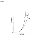
- the MIM elements, the MIS elements and the other two-terminal active elements do not have necessarily an invariable single I-V characteristic as shown in Fig. 2, but have a characteristic which varies in accordance with a continually-applied voltage V as shown in Figs. 5 and 6.
- Fig. 5 shows variation of the I-V characteristic with an applied voltage, in which an initial I-V characteristic as indicated by a solid line c is changed to that as indicated by a dotted line d due to a continually-applied voltage V
- Fig. 6 shows a variation amount (hereinafter referred to as "shift amount") of the I-V characteristic with variation of a voltage-applying time for each applied voltage.
- shift amount variation amount
- the initial I-V characteristic is varied to that as indicated by the dotted line d of Fig. 6 after a time elapses, and stabilized to the I-V characteristic after the variation.
- shift characteristic differs in accordance with difference in applied voltage V (for example, in Fig. 6, the voltage V satisfies the following inequality: p>r>n>f, and the shift characteristics of the respective I-V characteristics are different from each other).
- a time required for the I-V characteristic varied due to the continually-applied voltage to return to the initial I-V characteristic is longer as the shift amount (the variation amount as indicated by an arrow of Fig. 5) is increased.
- the shift characteristic is described in more detail in "E. Mizobatta, et al: SID 91 Digest, p.226 (1991)" or other papers.
- the shift characteristic causes the occurrence of an afterimage on the liquid crystal panel.
- a window pattern having a white portion at the center portion thereof and a black portion surrounding the white portion is first displayed on the liquid crystal panel as shown in Fig. 7(a), and then is changed to an overall white pattern (white raster).
- the first displayed window pattern is not completely erased, and it is left behind as an afterimage on the liquid crystal panel as shown in Fig. 7(b), so that the overall white pattern is not obtained on the liquid crystal panel.
- This so-called afterimage phenomenon is gradually extinguished as a long time elapses, but the display quality is remarkably degraded.
- the white display portion is supplied with a difference signal of applied voltage n as show in Fig. 7(c) for the selection period T S , while the black display portion is supplied with a difference signal of applied voltage f (f ⁇ n) for the selection period T S . Therefore, the two-terminal active element located at the white display portion is supplied with a higher voltage than that located at the black display portion, so that apparently from Figs.
- the shift amount of the I-V characteristic of the two-terminal active element at the white display portion is larger than that of the two-terminal active element at the black display portion.
- the afterimage as shown in Fig. 7(b) occurs due to the difference of the shift amounts of the two-terminal active elements at the white and black display portions.
- the afterimage phenomenon also occurs in a case where a window pattern having a white portion at the center portion of the liquid crystal panel and a black portion surrounding the white portion is first displayed on the liquid crystal panel, and then the whole screen of the liquid crystal panel is changed from the above display pattern to a display pattern having a half tone, and also in a case where a pattern having a half tone is first displayed on the liquid crystal panel, and then the display pattern is changed from the above pattern to a pattern having different half tone which is set with a lower voltage that the former pattern.
- the afterimage phenomenon due to such an display pattern changing operation to a half tone pattern will be described in more detail.
- the following assumption is introduced.
- the black portion P1 is formed by a difference signal (VX m1 - HY n ) which is applied through the column electrode X m1 and the row electrode Y n
- the white portion P2 is formed by a difference signal (VX m2 - HV n ) which is applied through the column electrode X m2 and the row electrode Y n
- the display pattern changing operation to a half tone pattern is carried out by applying difference signals (VX m1 - HY n ) and (VX m2 - HV n ) which are equal to each other, so that an afterimage occurs in which the central portion P2 is darker than the surrounding portion P1 as shown in Fig. 9.
- the difference signals (VX m1 - HY n ) and (VX m2 - HY n ) are applied in accordance with timing charts as shown in Fig. 10. That is, for each selection period T S (in a case of_normally black display) within a period for which black and white are displayed, the voltage V mSB of the difference signal (VX m1 - HY n ) which is applied to the two-terminal active elements for the black portion P1 is lower than the voltage V msW of the difference signal (VX m2 - HY n ) which is applied to the two-terminal active elements for the white portion P2. Therefore, apparently from Figs.
- the shift amount of the two-terminal active element for the portion P2 is larger than that of the two-terminal active element for the portion P1.
- the internal impedance of the two-terminal active element for the portion P2 is increased while the internal impedance of the two-terminal active element for the portion P1 is lower than the former, and this characteristic is maintained.
- the amount of charges Q2 flowing into the liquid crystal layer through the two-terminal active element for the portion P2 is smaller that the amount of charges Q1 flowing into the liquid crystal layer through the two-terminal active element for the portion P1 within a half tone display period although the voltage V ms1 of the difference signal (VX m1 - HY n ) and the voltage V ms2 of the difference signal (VX m2 - HY n ) which are supplied for the selection period T S are voltages for the same half tone.
- the effective voltage (which is proportional to the charge amount Q2) applied to the liquid crystal layer for the portion P2 for a non-selection period T N within the half tone display period is represented by an oblique portion S2 in Fig. 10 while the effective voltage (which is proportional to the charge amount Q1) applied to the liquid crystal layer for the portion P1 is represented by an oblique portion in Fig. 10, and thus the following inequality is apparently satisfied: S1 > S2. Therefore, a dark afterimage is formed at the portion P2 while a predetermined half tone image is formed at the portion P1. Such an afterimage phenomenon is called a "sticking phenomenon".
- a first embodiment of the driving method according to this invention will be next described with reference to Figs. 11 through 16.
- the first embodiment has been implemented in view of the degradation of display quality due to the shift characteristic in which the I-V characteristic of the two-terminal active element is shifted in accordance with a voltage applied to the two-terminal active element and can prevent occurrence of the afterimage phenomenon by compensating the shift characteristic of the two-terminal active element in a display operation of the liquid crystal panel of the liquid crystal display device.
- the liquid crystal display device is equipped with a liquid crystal panel 400, an X-drive circuit 500 and a Y-drive circuit 600, and performs a display operation through a line-sequential scanning of the picture elements of the liquid crystal panel 400 by the X-drive circuit 500 and the Y-drive circuit 600.
- the liquid crystal panel 400 includes a set of plural column electrodes X 1 through X m to X M (in figure, a m-th column electrode X m is representatively represented) which are connected to the X-drive circuit 500, another set of plural row electrodes Y 1 through Y n to Y N (in figure, n-th row electrode Y n is representatively represented) which are connected to the Y-drive circuit 600, the set of column electrodes and the set of row electrodes being provided on respective facing substrates so as to intersect each other, liquid crystal filled in a space between the column electrodes X 1 through X m to X M and the row electrodes Y 1 through Y n to Y N , and two-terminal active elements each provided at each intersecting portion (picture element portion) between the column electrode and the row electrode).
- a liquid crystal layer 401 serving as a picture element and a two-terminal type active element 402 are connected in series between the column electrode X m and the row electrode Y n , and both of a voltage V 1 to be applied to the liquid crystal layer 401 and a voltage V m to be applied to the two-terminal active element 402 are determined in accordance with a difference signal (VX m - HY n ) to be applied between the electrodes X m and Y n .
- the X-drive circuit 500 is equipped with an X shift register 501 having output contact points of M for the column electrodes X 1 through X m to X M , a set of latch circuits (in figure, the latch circuit 502 for the m-th column electrode X m is representatively shown), and a set of column electrode driving circuits (in figure, the column electrode driving circuit 503 for the m-th column electrode X m is representatively shown), these sets being provided between these output contact points and the set of the column electrodes X 1 through X m to X M .
- An A/D converter 700 receives the video signal P, and converts it to N-bit digital video data in which the maximum gradation is represented by (2 N -1).
- the converted digital video data is supplied to the X shift register 501.
- the X shift register 501 is supplied with the digital video data in synchronism with the shift clock signal X SCL of predetermined frequency f x , and is equipped with an M-stage shift register for performing a parallel shifting operation every N bits, thereby successively outputting digital video data D 1 through D m to D M from the output contact points in synchronism with the shift clock signal X SCL .
- a set of latch circuits and a set of driving circuits are provided between the column electrodes X 1 through X m to X M and the output contacts of the X shift register 501.
- the following description is made representatively for a latch circuit 502 and a driving circuit 503 for the m-th column electrode X m .
- the latch circuit 502 latches a digital video data D m outputted from the X shift register 501 in synchronism with an output timing.
- the driving circuit 503 carries out a pulse-width modulation processing to output to the column electrode X m a column electrode signal VX m having a time width which is proportional to a gradation set or represented by the digital video data D m .
- the a.c. inversion signal FR is formed of a rectangular waveform having 50% duty factor and each half period thereof corresponds to one horizontal scanning period, so that the a.c. inversion signal FR serves to set the selection period T S for which the row electrodes Y 1 to Y N are successively selected at the timing of the line-sequential scanning operation.
- a selection period for negative polarity (negative-polarity selection period) T S is set up when the a.c.
- inversion signal FR has the logical value "H", while a selection period for positive polarity (positive-polarity selection period) T S is set up when the a.c. inversion signal FR has the logical value "L".
- the maximum gradation (2 N - 1) of the digital video data D m is set to be equal to the time width of the half period (i.e., T S ) of the a.c. inversion signal FR, and the pulse width modulation (PWM modulation) is carried out within this time width. Further, when the a.c.
- the column electrode signal VX m is set to V a for the time width T on which is proportional to the digital video data D m , and is set to - V a for the residual time width T off .
- the column electrode signal VX m is set to -V a for a selection time width T on corresponding to the digital video data D m and is set to V a for the residual time width T off .
- a liquid crystal power generating circuit 601 in the Y-drive circuit 600 is supplied with six kinds of voltages V r , V p , V a , -V r , -V p , -V a whose absolute values satisfy the following inequality:
- the Y shift register 605 shifts the Y shift start signal DY in synchronism with the shift clock signal Y SCL of predetermined frequency f Y to successively output the selection signals C 1 through C n to C N from the output contact points of N.
- a set of switching circuits are provided between the respective output contact points of the Y shift register 605 and the row electrodes Y 1 through Y n to Y N .
- the following description is made representatively for a switching circuit for an n-th row electrode Y n .
- the switching circuit includes an AND gate 606 for obtaining a logical product between a selection signal C n outputted from an n-th output contact point of the Y shift register 605 and a selection signal C n-1 outputted from an (n-1)-th output contact point which is located just prior to the n-th output contact point, an AND gate 607 for obtaining a logical product between the selection signal C n outputted from the n-th output contact point and a logically-inverted signal of the selection signal C n-1 outputted from the (n-1)-th output contact point which is located just prior to the n-th output contact point, an analog switch 608 which is provided between the transmission line 602 and the row electrode Y n and switched between conducting and non-conducting states in accordance with the logical output of the AND gate 606, an analog switch 609 which is provided between the transmission line 603 and the row electrode Y n and switched between conducting and non-conducting states in accordance with the logical output of the AND gate 607, and
- inversion signal FR has the logical value "H”
- the selection signal C n-1 has the logical value “L”
- the selection signal C n has the logical value "H”
- the selection voltage +V P is applied to the row electrode Y n
- the selection signal C n-1 has the logical value "L”
- the selection signal C n has the logical value "H”
- the selection voltage -V P is applied to the row electrode Y n .
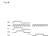
- the time width of the shift start signal DY is set to a period corresponding to four periods of the shift clock signal Y SCL .
- the shift start signal DY is successively shifted in synchronism with the trailing edge of the shift clock signal Y SCL in the Y shift register 605 to thereby generate selection signals C 1 to C N which have the same time width as the shift start signal DY and are deviated from one another by one period of the shift clock signal Y SCL .
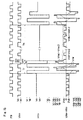
- a difference signal to be applied to each of m1-th and m2-th column electrodes X m1 and X m2 for an n-th row electrode Y n has a waveform as shown in Fig. 15.
- a period T r for which the logical values of both of the selection signals C n-1 and C n are "H” is three times of the horizontal scanning period (3H).
- the electrodes are supplied with a larger voltage than the maximum-amplitude voltage used for an ordinary display operation (the maximum amplitude voltage is equal to V p + V a for black at the positive polarity, and is equal to - (V p + V a ) for black at the negative polarity.
- a next one-horizontal period subsequent to the reset period T r corresponds to an ordinary selection period T s , and the column electrode signal VX m outputted from the X-drive circuit 500 is supplied to the column electrode X m .
- the selection period T s is completed, a next scanning operation of the row electrode is started, and thus this period is a non-selection period T N for the row electrode Y n .
- This non-selection period T N is continued until one-field scanning period or one-frame scanning period elapses. Thereafter, upon completion of the one-field or one-frame scanning period, the non-selection period T N is transferred to the reset period T r and the selection period T S , and these processings are repeated. The same processings are conducted on the other scanning operations of the other column electrodes C 1 to C n+1 and C n+1 to C N .
- the polarity of the voltage to be applied to each of the column electrodes c 1 to C N is inverted every one-field or one-frame scanning period.
- a picture element at an intersecting portion (ml, n) between the ml-th column electrode X m1 and the n-th row electrode Y n is supplied with a difference signal (VX m1 - HY n ) having an absolute value
- a picture element at an intersecting portion (m2, n) between the m2-th column electrode X m2 and the n-th row electrode Y n is supplied with a difference signal (VX m2 - HY n ) having an absolute value
- the picture elements (m1,n) and (m2,n) are switched from the above display states to a half tone display state for a half tone display period.
- the difference signal (VX m1 - HY n ) applied to the picture element at the intersecting portion between the column electrode X m1 and the row electrode Y n is equal to the difference signal (VX m2 - HY n ) applied to the picture element at the intersecting portion between the column electrode X m2 and the row electrode Y n , however, the effective voltages V ms1 and V ms2 applied to the liquid crystal layer, and the effective values S1 and S2 are respectively different from each other as shown in Fig. 15 due to the difference in shift characteristic which is caused by the white and black display operations.
- This difference in shift characteristic causes an afterimage.
- the following description is the principle of greatly depressing the afterimage phenomenon by applying a difference signal of large voltage in the reset period T r just before the ordinary selection period T S .
- the cause of occurrence of the afterimage resides in that there is a difference in shift amount of electrical characteristic between two-terminal active elements used for the picture elements which are carrying out white and black display operations, respectively, and thus the effective voltages to be applied to the liquid crystal layer are different between these two-terminal active elements due to the difference of the characteristics thereof even when both of the two-terminal active elements are driven to carry out the same half tone display operation.
- a difference signal having high voltage is applied to a two-terminal active element for the reset period T r to thereby saturate the I-V shift characteristic of the two-terminal active element with the high voltage and hold the I-V shift characteristic, so that the I-V characteristic of the two-terminal active element is not fluctuated since then.
- the two-terminal active element carries out a display operation on the basis of the stabilized I-V shift characteristic which has been subjected to the above saturation treatment with the high voltage, so that the occurrence of the afterimage phenomenon which has been conventionally caused due to the shift characteristic can be greatly depressed.
- Fig. 16 is an enlarged view of the timing chart within the half tone display period as shown in Fig. 15.
- Fig. 16 shows representatively the column electrode signal VX m and the row electrode signal HY n which are applied to the m-th column electrode X m and the n-th row electrode Y n respectively, and the difference signal (VX m - HY n ).
- a waveform indicated by a solid line represents an actually-applied voltage
- a waveform indicated by a dotted line represents an effective voltage.
- the voltage V ms1 of the difference signal (VX m - HY n ) and the effective voltage V mn1 are voltages before one-field or one-frame period
- the voltage V ms2 of the difference signal (VX m - HY n ) and the effective voltage V mn2 are voltages after one-field or one-frame period.
- the voltages V ms1 , V 1s1 , V mn1 and S1 represent voltages which are applied to the liquid crystal layer and the two-terminal active element for the half tone display state after the black display period
- the voltages V ms2 , V 1s2 , V mn2 and S2 are voltages which are applied to the liquid crystal layer and the two-terminal active element for the half tone display state after the white display period, these voltages being superposedly shown on the same time axis
- the reset period T r is circulatingly provided to each of the row electrodes Y 1 to Y N every one-field or one-frame period, and thus the reset period T r every three horizontal scanning periods (3H) merely corresponds to a period of several % of the one-field or one-frame period. Accordingly, the fluctuation of the voltage applied to the liquid crystal layer is remarkably slight even when the high voltage is applied to the liquid crystal layer for the reset period T r according to the driving method of this embodiment, and thus the application of the high voltage to the liquid crystal layer never causes the degradation of display quality.
- the reset period T r is set to three-horizontal scanning periods.
- the reset period T r is not necessarily limited to this value, and may be set to a period longer than the above period insofar as the degradation of display quality due to the voltage fluctuation is not induced.
- the reset period T r may be shorter than that of this embodiment by increasing the applied voltage in the reset period T r . In this case, it is needless to say that the maximum value of the voltage must be set to such a value that the liquid crystal layer and the two-terminal active element are not damaged.
- FIG. 17 A second embodiment of this invention will be next described with reference to Figs. 17 through 20.
- this embodiment has been implemented in view of the problem of the degradation of the display quality due to the shift characteristic that the I-V characteristic is shifted in accordance with the voltage applied to the two-terminal active element, and can prevent the occurrence of the afterimage phenomenon by compensating for the shift characteristic of the two-terminal active element in the display operation of the liquid crystal panel of the liquid crystal display device.
- Fig. 17 the same or substantially same portions as those of Fig. 11 are represented by the same reference numerals.
- the liquid crystal display device of this embodiment is equipped with the liquid crystal panel 400, the X-drive circuit 500 and the Y-drive circuit 600, and the display operation is carried out through the line-sequential scanning operation of the respective picture element portions of the liquid crystal panel 400 using the X-drive circuit 500 and the Y-drive circuit 600.
- the liquid crystal panel 400 includes a set of plural column electrodes X 1 through X m to X M (in figure, a m-th column electrode X m is representatively represented) which are connected to the X-drive circuit 500, another set of plural row electrodes Y 1 through Y n to Y N (in figure, n-th row electrode Y n is representatively represented) which are connected to the Y-drive circuit 600, the set of column electrodes and the set of row electrodes being provided on respective facing substrates so as to be intersected to each other, liquid crystal filled in a space between the column electrodes X 1 through X m to X M and the row electrodes Y 1 through Y n to Y N , and two-terminal active elements each provided at each intersecting portion (picture element portion) between the column electrode and the row electrode).
- a liquid crystal layer 401 serving as a picture element and a two-terminal type active element 402 are connected in series between the column electrode X m and the row electrode Y n .
- the X-drive circuit 500 is equipped with an X shift register 501 having output contact points of M for the column electrodes X 1 through X m to X M , a set of latch circuits (in figure, the latch circuit 502 for the m-th column electrode X m is representatively shown), and a set of column electrode driving circuits (in figure, the column electrode driving circuit 503 for the m-th column electrode X m is representatively shown), these sets being provided between these output contact points and the set of the column electrodes X 1 through X m to X M .
- An A/D converter 700 receives the video signal P, and converts it to an N-bit digital video data in which the maximum gradation is represented by (2 N -1).
- the converted digital video data is supplied to the X shift register 501.
- the X shift register 501 is supplied with the digital video data in synchronism with shift clock signal X SCL of predetermined frequency f X , and is equipped with an M-stage shift register for performing a parallel shifting operation every N bits, thereby successively outputting digital video data D 1 through D m to D M from the output contact points in synchronism with the shift clock signal X SCL .
- a set of latch circuits and a set of driving circuits are provided between the column electrodes X 1 through X m to X M and the output contacts of the X shift register 501.
- the following description is made representatively for a latch circuit 502 and a driving circuit 503 for the m-th column electrode X m .
- the latch circuit 502 latches a digital video data D m outputted from the X shift register 501 in synchronism with an output timing.
- the driving circuit 503 carries out a pulse-width modulation processing to output to the column electrode X m a column electrode signal VX m having a time width which is proportional to a gradation set by the digital video data D m .
- the pulse-width modulation processing is carried out in accordance with the same principle as in the first embodiment.
- the liquid crystal power generating circuit 601 in the Y-drive circuit 600 is supplied with four kinds of voltages V p , V a , -V p , -V a whose absolute values satisfy the following inequality:
- the Y shift register 605 shifts a Y shift start signal DY in synchronism with a shift clock signal Y SCL of predetermined frequency f Y to successively output selection signals C 1 through C n to C N from the output contact points of N.
- a set of switching circuits are provided between the output contact points and the row electrodes Y 1 through Y n to Y N .
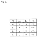
- the switching circuit includes a first analog switch 613 whose conducting and non-conducting states are switched in accordance with the selection signal C n outputted from the n-th output contact point of the Y shift register 605, and which is connected between the transmission line 611 and the row electrode Y n , and a second switch whose conducting and non-conducting states are switched in accordance with an inversion signal of the selection signal C n and which is connected between the transmission line 612 and the row electrode Y n .
- the liquid crystal voltage V n is supplied to the row electrode Y n
- the selection signal C n has a logical value "L”
- the liquid crystal voltage V N is supplied to the row electrode Y n .
- the time width of the shift start signal DY is set to a value corresponding to four periods of the shift clock signal Y SCL .
- the shift start signal DY is successively shifted in synchronism with the trailing edge of the shift clock signal Y SCL , thereby generating the selection signals C 1 to C N which have the same time width as the shift start signal DY and are deviated from one another by one period of the shift clock signal Y SCL .
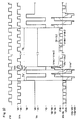
- difference signals (VX m1 - HY n ) and (VX m2 - HY n ) which are applied to the ml-th and m2-th column electrodes X m1 and X m2 for the n-th row electrode, respectively, have waveforms as shown in Fig. 19.
- a period T S ' for which the selection signal C n has the logical value "H" (hereinafter referred to as "reset period") is equal to three times of the horizontal scanning period (3H).
- a period subsequent to the reset period T S ' corresponds to an ordinary selection period T S , and the column electrode signal VX m outputted from the X-drive circuit 500 is supplied to the column electrode X m . Further, when the selection period T S is completed, the scanning operation of the next row electrode is started, and this period is a non-selection period for the row electrode Y n . The non-selection period T N is continued until one-field or one-frame scanning period elapses. Thereafter, the reset period T S ' and the selection period T S are returned again, and these processings are repeated. The same processings are repeated for the scanning operation of the other column electrodes C 1 to C n-1 and C n+1 to C N .
- the polarity of the voltage applied to each of the column electrodes C 1 to C N is inverted every one-field or one-frame scanning period.
- Fig. 19 shows a situation where a picture element (m1,n) at the intersecting portion between the m1-th column electrode X m1 and the n-th row electrode Y n is supplied with the difference signal (VX m1 - HY n ) having the voltage
- the effective voltages of the difference signals (VX m1 - HY n ) and (VX m2 - HY n ) are equal to V ms1 and V ms2 respectively for the selection period T S within the half tone display period, and the effective voltages in the non-selection period T N are equal to S1 and S2.
- the difference signal (VX m1 - HY n ) applied to the picture element at the intersecting portion between the column electrode X m1 and the row electrode Y n is equal to the difference signal (VX m2 - HY n ) applied to the picture element at the intersecting portion between the column electrode X m2 and the row electrode Y n , however, the effective voltages V ms1 and V ms2 applied to the liquid crystal layer, and the effective values S1 and S2 are respectively different from each other as shown in Fig. 19 due to the difference in shift characteristic which is caused by the white and black display operations.
- This difference in shift characteristic causes an afterimage phenomenon.
- the following description is the principle of greatly depressing the afterimage phenomenon by applying a difference signal of large voltage in the reset period T S ' just before the ordinary selection period T S .
- the cause of occurrence of the afterimage resides in that there is a difference in shift amount of electrical characteristic between two-terminal active elements used for the picture elements which are carrying out white and black display operations, respectively, and thus the effective voltages to be applied to the liquid crystal layer are different between these two-terminal active elements due to the difference of the characteristics thereof even when both of the two-terminal active elements are driven to carry out the same half tone display operation.
- a difference signal having high voltage is applied to a two-terminal active element for the reset period T S ' to thereby saturate the I-V shift characteristic of the two-terminal active element with the high voltage and hold the I-V shift characteristic, so that the I-V characteristic of the two-terminal active element is not fluctuated since then.
- the two-terminal active element carries out a display operation on the basis of the stabilized I-V characteristic, so that the occurrence of the afterimage phenomenon which has been conventionally caused due to the shift characteristic can be greatly depressed.
- Fig. 20 is an enlarged view of the timing chart within the half tone display period as shown in Fig. 19.
- Fig. 20 shows representatively the column electrode signal VX m and the row electrode signal HY n which are applied to the m-th column electrode X m and the n-th row electrode Y n respectively, and the difference signal (VX m - HY n ).
- a waveform indicated by a solid line represents an actually-applied voltage
- a waveform indicated by a dotted line represents an effective voltage.
- the voltage V ms1 of the difference signal (VX m - HY n ) and the effective voltage V mn1 are voltages before one-field or one-frame period
- the voltage V ms2 of the difference signal (VX m - HY n ) and the effective voltage V mn2 are voltages after one-field or one-frame period.
- the voltages V ms1 , V 1s1 , V mn1 and S1 represent voltages which are applied to the liquid crystal layer and the two-terminal active element for the half tone display state after the black display period
- the voltages V ms2 , V 1s2 , V mn2 and S2 are voltages which are applied to the liquid crystal layer and the two-terminal active element for the half tone display state after the white display period, these voltages being superposedly shown on the same time axis.
- the reset period T S ' is circulatingly provided to each of the row electrodes Y 1 to Y N every one-field or one-frame period, and thus the reset period T S ' every three horizontal scanning periods (3H) merely corresponds to a period of several % of the one-field or one-frame period. Accordingly, the fluctuation of the voltage applied to the liquid crystal layer is remarkably slight even when the high voltage is applied to the liquid crystal layer for the reset period T S ' according to the driving method of this embodiment, and thus the application of the high voltage to the liquid crystal layer never causes the degradation of display quality.
- the reset period T S ' is set to three-horizontal scanning period.
- the reset period T S ' is not necessarily limited to this value, and may be set to a period above the above period or any value insofar as the degradation of display quality due to the voltage fluctuation is not induced. Further, the reset period T S ' may be shorter than that of this embodiment by increasing the applied voltage in the reset period T S '.
- the high voltage as used in the first embodiment is not applied for the reset period in the second embodiment, and thus it is not required to apply an excessive voltage to the liquid crystal layer and the two-terminal active element, so that the deterioration of the liquid crystal panel with time lapse can be prevented.
- a power generator for independently generating a high voltage for a reset operation is not required, so that the switching circuit provided between the Y shift register 605 and the row electrodes Y 1 to Y N can be simplified in construction.
- a third embodiment of this invention will be next described with reference to Figs. 21 through 23.
- this embodiment has been implemented in view of the problem of the degradation of display quality due to the shift characteristic that the I-V characteristic is shifted in accordance with the voltage applied to the two-terminal active element.
- the occurrence of the afterimage phenomenon is prevented by compensating for the shift characteristic of the two-terminal active element for a period except for an actual displaying operation period.
- the construction of the active matrix type liquid crystal display device has the same construction as that of Fig. 11.
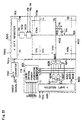
- the set of driving circuits (in figure, a driving circuit 503 is representatively shown) provided in the X-drive circuit 500 is supplied with six kinds of voltages V r /2, V p /2, V a /2, -V r /2,-V p /2, -V a /2, in place of the voltages V a and -V a .
- the liquid crystal power generating circuit 601 is supplied with V r /2, V p /2, V a /2, -V r /2, -V p /2,-V a /2, in place of the voltages V r , V p , V a , -V r , -V p , -V a .
- These voltages satisfy the following inequality:
- a period from the time when a power of the liquid crystal display device is switched on by an user or the like until the time when an actual displaying operation starts is defined as a refresh period T R
- a period for which the actual display operation is carried out after the refresh period T R is defined as a display period T D .
- a video signal is subjected to the pulse width modulation to be converted to rectangular column electrode signals VX 1 to VX M , and these converted column electrode signals are supplied to the column electrodes X 1 to X n in synchronism with the timing of the linesequential scan.
- rectangular row electrode signals HY 1 to HY N as shown in Fig. 22(b) are supplied to the row electrodes Y 1 to Y N in synchronism with the timing of the line-sequential scan.
- a difference signal as shown in Fig. 21 is formed for the display period T D .
- one-frame period, one-field period and one-horizontal period are represented by 1F, 1V and 1H.
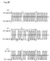
- the row electrode signals HY 1 to HY N applied to the row electrodes Y 1 to Y N are deviated in phase from the row electrode signals as shown in Fig. 22(b) by 180°, and thus voltages of (V r + V a )/2 and -(V r + V a ) are outputted in place of (V p + V a )/2 and -(V p + V a ). Simultaneously with the application of the row electrode signals HY 1 to HY N as shown in Fig.
- the column electrode signals VX 1 to VX M which have rectangular forms as shown in Fig. 22(a) and output voltages of (V r + V a )/2, (V r - V a )/2, -(V r - V a )/2, -(V r - V a )/2 (in place of (V r + V a )/2, (V p - V a )/2, -(V p - V a )/2, -(V r - V a )/2) are applied, thereby obtaining difference signals having waveforms as shown in Fig. 23(b).
- the difference signal as shown in Fig. 23(b) corresponds to the signal in the refresh period T R as shown in Fig. 21.
- a high voltage is also beforehand applied between the set of column electrodes and the set of row electrodes for the refresh period T R to shift the I-V characteristic of the two-terminal active element to the I-V characteristic at the high voltage region, so that the I-V characteristic is fixed for a next normal display period T D . Therefore, the accumulation of the d.c. offset component is prevented, and thus the occurrence of the afterimage phenomenon can be depressed.
- a fourth embodiment will be next described with reference to Fig. 24.
- the active matrix type liquid crystal display device to which this embodiment is applied has the same construction as the third embodiment (see Fig. 11).
- the feature of this embodiment resides in that the waveform of a difference signal having high amplitude voltage applied for the refresh period T R is designed so as to have a completely rectangular waveform as shown in Fig. 24(c).
- a waveform as shown in Fig. 24(a) is assigned to the column electrode signals VX 1 to VX M while a waveform as shown in Fig. 24(b) is assigned to the row electrode signals HY 1 to HY N .
- one-frame period, one-field period and one-horizontal period are represented by 1F, 1V and 1H, respectively.
- a high voltage can be easily obtained, and the compensation of the electrical characteristic of the two-terminal active element can be easily performed.
- the active matrix type liquid crystal display device of this embodiment has the same construction as the third embodiment (see Fig. 11).
- the refresh period T R is suitably inserted in the display period T D to periodically compensate for the shift characteristic of the two-terminal active element. According to this method, the compensating operation is periodically carried out and thus the shift characteristic of the two-terminal active element can be surely compensated.
- the refresh period T R is set to an excessively long time, then the normal display period T D would be damaged, and thus the refresh period T r is preferably inserted every several seconds, one-horizontal scanning period or one-vertical scanning period.
Landscapes
- Engineering & Computer Science (AREA)
- Chemical & Material Sciences (AREA)
- Crystallography & Structural Chemistry (AREA)
- Physics & Mathematics (AREA)
- Computer Hardware Design (AREA)
- General Physics & Mathematics (AREA)
- Theoretical Computer Science (AREA)
- Liquid Crystal Display Device Control (AREA)
- Liquid Crystal (AREA)
- Control Of Indicators Other Than Cathode Ray Tubes (AREA)
Priority Applications (1)
| Application Number | Priority Date | Filing Date | Title |
|---|---|---|---|
| EP95113259A EP0697690B1 (en) | 1991-03-20 | 1992-03-20 | Method for driving active matrix type liquid crystal display device |
Applications Claiming Priority (8)
| Application Number | Priority Date | Filing Date | Title |
|---|---|---|---|
| JP5715291 | 1991-03-20 | ||
| JP57152/91 | 1991-03-20 | ||
| JP15031591 | 1991-06-21 | ||
| JP150315/91 | 1991-06-21 | ||
| JP19675391 | 1991-08-06 | ||
| JP196753/91 | 1991-08-06 | ||
| JP196754/91 | 1991-08-06 | ||
| JP19675491 | 1991-08-06 |
Related Child Applications (1)
| Application Number | Title | Priority Date | Filing Date |
|---|---|---|---|
| EP95113259.6 Division-Into | 1992-03-20 |
Publications (3)
| Publication Number | Publication Date |
|---|---|
| EP0508628A2 EP0508628A2 (en) | 1992-10-14 |
| EP0508628A3 EP0508628A3 (en) | 1993-02-03 |
| EP0508628B1 true EP0508628B1 (en) | 1997-06-11 |
Family
ID=27463456
Family Applications (2)
| Application Number | Title | Priority Date | Filing Date |
|---|---|---|---|
| EP92302419A Expired - Lifetime EP0508628B1 (en) | 1991-03-20 | 1992-03-20 | Method for driving active matrix type liquid crystal display device |
| EP95113259A Expired - Lifetime EP0697690B1 (en) | 1991-03-20 | 1992-03-20 | Method for driving active matrix type liquid crystal display device |
Family Applications After (1)
| Application Number | Title | Priority Date | Filing Date |
|---|---|---|---|
| EP95113259A Expired - Lifetime EP0697690B1 (en) | 1991-03-20 | 1992-03-20 | Method for driving active matrix type liquid crystal display device |
Country Status (4)
| Country | Link |
|---|---|
| US (1) | US5526013A (online.php) |
| EP (2) | EP0508628B1 (online.php) |
| DE (2) | DE69222959T2 (online.php) |
| TW (1) | TW200572B (online.php) |
Families Citing this family (19)
| Publication number | Priority date | Publication date | Assignee | Title |
|---|---|---|---|---|
| US6271817B1 (en) | 1991-03-20 | 2001-08-07 | Seiko Epson Corporation | Method of driving liquid crystal display device that reduces afterimages |
| US5790089A (en) * | 1991-03-20 | 1998-08-04 | Seiko Epson Corporation | Method of driving an active matrix type liquid crystal display |
| JP3482667B2 (ja) * | 1993-01-13 | 2003-12-22 | セイコーエプソン株式会社 | 液晶表示装置の駆動方法及び液晶表示装置 |
| US5666131A (en) * | 1992-06-19 | 1997-09-09 | Citizen Watch Co., Ltd. | Active matrix liquid-crystal display device with two-terminal switching elements and method of driving the same |
| JP3167135B2 (ja) * | 1992-06-19 | 2001-05-21 | シチズン時計株式会社 | 2端子型アクティブマトリクス液晶表示装置及びその駆動方法 |
| US5561441A (en) * | 1993-04-08 | 1996-10-01 | Citizen Watch Co., Ltd. | Liquid crystal display device |
| DE69322154T2 (de) * | 1993-04-08 | 1999-07-01 | Citizen Watch Co., Ltd., Tokio/Tokyo | Verfahren zur Steuerung einer Flüssigkristallanzeigetafel |
| JP3133215B2 (ja) * | 1994-07-15 | 2001-02-05 | シャープ株式会社 | 表示装置の駆動方法 |
| JPH08129360A (ja) * | 1994-10-31 | 1996-05-21 | Tdk Corp | エレクトロルミネセンス表示装置 |
| US6853083B1 (en) * | 1995-03-24 | 2005-02-08 | Semiconductor Energy Laboratory Co., Ltd. | Thin film transfer, organic electroluminescence display device and manufacturing method of the same |
| JP3135819B2 (ja) * | 1995-04-25 | 2001-02-19 | シャープ株式会社 | 液晶表示装置の駆動方法 |
| JP3854329B2 (ja) * | 1995-12-27 | 2006-12-06 | シャープ株式会社 | マトリクス型表示装置の駆動回路 |
| US6421038B1 (en) | 1998-09-19 | 2002-07-16 | Lg. Philips Lcd Co., Ltd. | Active matrix liquid crystal display |
| KR100700415B1 (ko) * | 1998-09-19 | 2007-03-27 | 엘지.필립스 엘시디 주식회사 | 액티브 매트릭스 액정표시장치 |
| US7002542B2 (en) | 1998-09-19 | 2006-02-21 | Lg.Philips Lcd Co., Ltd. | Active matrix liquid crystal display |
| TW591590B (en) * | 2003-04-17 | 2004-06-11 | Hannstar Display Corp | Black image insertion method and apparatus for display |
| CN100412938C (zh) * | 2003-06-11 | 2008-08-20 | 瀚宇彩晶股份有限公司 | 插入黑画面的显示方式与装置 |
| JP2010128365A (ja) * | 2008-11-28 | 2010-06-10 | Fujitsu Ltd | 表示装置 |
| JP5552954B2 (ja) * | 2010-08-11 | 2014-07-16 | セイコーエプソン株式会社 | 電気光学装置および電子機器 |
Family Cites Families (10)
| Publication number | Priority date | Publication date | Assignee | Title |
|---|---|---|---|---|
| JPS5758190A (en) * | 1980-09-25 | 1982-04-07 | Suwa Seikosha Kk | Active matric type liquid crystal indicator driving system |
| JPS5821793A (ja) * | 1981-07-31 | 1983-02-08 | セイコーエプソン株式会社 | 液晶表示装置 |
| GB2173335B (en) * | 1985-04-03 | 1988-02-17 | Stc Plc | Addressing liquid crystal cells |
| NL8701420A (nl) * | 1987-06-18 | 1989-01-16 | Philips Nv | Weergeefinrichting en werkwijze voor het besturen van een dergelijke weergeefinrichting. |
| US5117298A (en) * | 1988-09-20 | 1992-05-26 | Nec Corporation | Active matrix liquid crystal display with reduced flickers |
| NL8802436A (nl) * | 1988-10-05 | 1990-05-01 | Philips Electronics Nv | Werkwijze voor het besturen van een weergeefinrichting. |
| GB2223618A (en) * | 1988-10-07 | 1990-04-11 | Philips Electronic Associated | Display devices |
| JPH02135419A (ja) * | 1988-11-17 | 1990-05-24 | Seiko Epson Corp | 液晶表示装置の駆動法 |
| JPH02187789A (ja) * | 1989-01-13 | 1990-07-23 | Matsushita Electric Ind Co Ltd | アクティブマトリクス型液晶表示装置 |
| JPH02187788A (ja) * | 1989-01-13 | 1990-07-23 | Matsushita Electric Ind Co Ltd | アクティブマトリクス型液晶表示装置 |
-
1992
- 1992-03-20 DE DE69222959T patent/DE69222959T2/de not_active Expired - Fee Related
- 1992-03-20 TW TW081102104A patent/TW200572B/zh active
- 1992-03-20 EP EP92302419A patent/EP0508628B1/en not_active Expired - Lifetime
- 1992-03-20 DE DE69220283T patent/DE69220283T2/de not_active Expired - Fee Related
- 1992-03-20 EP EP95113259A patent/EP0697690B1/en not_active Expired - Lifetime
-
1994
- 1994-08-23 US US08/294,878 patent/US5526013A/en not_active Expired - Fee Related
Non-Patent Citations (2)
| Title |
|---|
| PATENT ABSTRACTS OF JAPAN, unexamined applications, P field, vol. 14, no. 468, October 12, 1990 THE PATENT OFFICE JAPANESE GOVERNMENT page 146 P 1115 * Kokai-no. 2-187 788 (MATSUSHITA). * |
| PATENT ABSTRACTS OF JAPAN, unexamined applications, P field, vol. 14, no. 468, October 12, 1990 THE PATENT OFFICE JAPANESE GOVERNMENT page 146 P 1115 * Kokai-no. 2-187 789 (MATSUSHITA). * |
Also Published As
| Publication number | Publication date |
|---|---|
| DE69222959T2 (de) | 1998-03-19 |
| EP0697690B1 (en) | 1997-10-29 |
| TW200572B (online.php) | 1993-02-21 |
| US5526013A (en) | 1996-06-11 |
| DE69220283T2 (de) | 1997-10-30 |
| EP0508628A3 (en) | 1993-02-03 |
| DE69222959D1 (de) | 1997-12-04 |
| EP0697690A1 (en) | 1996-02-21 |
| DE69220283D1 (de) | 1997-07-17 |
| EP0508628A2 (en) | 1992-10-14 |
Similar Documents
| Publication | Publication Date | Title |
|---|---|---|
| US5526013A (en) | Method of driving an active matrix type liquid crystal display | |
| US5892504A (en) | Matrix display device and its method of operation | |
| US4795239A (en) | Method of driving a display panel | |
| US5598180A (en) | Active matrix type display apparatus | |
| EP0767449B1 (en) | Method and circuit for driving active matrix liquid crystal panel with control of the average driving voltage | |
| US20010010511A1 (en) | Active-matrix display device and method for driving the same | |
| US6566643B2 (en) | Electro-optical device, method of driving the same, and electronic apparatus using the same | |
| JPS59113420A (ja) | マトリクス表示装置の駆動方法 | |
| EP0656615B1 (en) | Active matrix liquid crystal display with improvements to the connection of the last line | |
| JPH0968689A (ja) | 液晶表示装置の駆動方法 | |
| US6829392B2 (en) | System and method for providing an image deghosting circuit in an electroptic display device | |
| US5790089A (en) | Method of driving an active matrix type liquid crystal display | |
| KR100864497B1 (ko) | 액정 표시 장치 | |
| JPH07318903A (ja) | 液晶表示装置及びその駆動方法 | |
| JPH01107237A (ja) | 液晶表示装置 | |
| JPH0683416B2 (ja) | 液晶表示装置用駆動回路 | |
| JPH07306660A (ja) | 液晶表示装置の階調駆動回路及びその階調駆動方法 | |
| EP0607860B1 (en) | Method of driving liquid crystal display device | |
| US6271817B1 (en) | Method of driving liquid crystal display device that reduces afterimages | |
| JPH04186282A (ja) | 多階調画像表示装置 | |
| JP3610074B2 (ja) | アクティブ・マトリクス型液晶表示装置の駆動方法 | |
| JPWO1995020209A1 (ja) | 液晶表示装置 | |
| WO1995020209A1 (en) | Liquid crystal display | |
| US5864327A (en) | Method of driving liquid crystal display device and liquid crystal display device | |
| JPH06301011A (ja) | マトリクス表示装置およびその駆動方法 |
Legal Events
| Date | Code | Title | Description |
|---|---|---|---|
| PUAI | Public reference made under article 153(3) epc to a published international application that has entered the european phase |
Free format text: ORIGINAL CODE: 0009012 |
|
| AK | Designated contracting states |
Kind code of ref document: A2 Designated state(s): DE FR GB |
|
| PUAL | Search report despatched |
Free format text: ORIGINAL CODE: 0009013 |
|
| AK | Designated contracting states |
Kind code of ref document: A3 Designated state(s): DE FR GB |
|
| 17P | Request for examination filed |
Effective date: 19930602 |
|
| 17Q | First examination report despatched |
Effective date: 19950216 |
|
| GRAG | Despatch of communication of intention to grant |
Free format text: ORIGINAL CODE: EPIDOS AGRA |
|
| GRAH | Despatch of communication of intention to grant a patent |
Free format text: ORIGINAL CODE: EPIDOS IGRA |
|
| GRAH | Despatch of communication of intention to grant a patent |
Free format text: ORIGINAL CODE: EPIDOS IGRA |
|
| GRAA | (expected) grant |
Free format text: ORIGINAL CODE: 0009210 |
|
| AK | Designated contracting states |
Kind code of ref document: B1 Designated state(s): DE FR GB |
|
| DX | Miscellaneous (deleted) | ||
| REF | Corresponds to: |
Ref document number: 69220283 Country of ref document: DE Date of ref document: 19970717 |
|
| ET | Fr: translation filed | ||
| PLBE | No opposition filed within time limit |
Free format text: ORIGINAL CODE: 0009261 |
|
| STAA | Information on the status of an ep patent application or granted ep patent |
Free format text: STATUS: NO OPPOSITION FILED WITHIN TIME LIMIT |
|
| 26N | No opposition filed | ||
| REG | Reference to a national code |
Ref country code: GB Ref legal event code: IF02 |
|
| PGFP | Annual fee paid to national office [announced via postgrant information from national office to epo] |
Ref country code: GB Payment date: 20080326 Year of fee payment: 17 |
|
| PGFP | Annual fee paid to national office [announced via postgrant information from national office to epo] |
Ref country code: DE Payment date: 20080313 Year of fee payment: 17 Ref country code: FR Payment date: 20080311 Year of fee payment: 17 |
|
| GBPC | Gb: european patent ceased through non-payment of renewal fee |
Effective date: 20090320 |
|
| REG | Reference to a national code |
Ref country code: FR Ref legal event code: ST Effective date: 20091130 |
|
| PG25 | Lapsed in a contracting state [announced via postgrant information from national office to epo] |
Ref country code: DE Free format text: LAPSE BECAUSE OF NON-PAYMENT OF DUE FEES Effective date: 20091001 |
|
| PG25 | Lapsed in a contracting state [announced via postgrant information from national office to epo] |
Ref country code: FR Free format text: LAPSE BECAUSE OF NON-PAYMENT OF DUE FEES Effective date: 20091123 Ref country code: GB Free format text: LAPSE BECAUSE OF NON-PAYMENT OF DUE FEES Effective date: 20090320 |