EP0507183A2 - Verfahren zur selektiven Ablagerung einer Schutzschicht aus Polymeren - Google Patents
Verfahren zur selektiven Ablagerung einer Schutzschicht aus Polymeren Download PDFInfo
- Publication number
- EP0507183A2 EP0507183A2 EP92105018A EP92105018A EP0507183A2 EP 0507183 A2 EP0507183 A2 EP 0507183A2 EP 92105018 A EP92105018 A EP 92105018A EP 92105018 A EP92105018 A EP 92105018A EP 0507183 A2 EP0507183 A2 EP 0507183A2
- Authority
- EP
- European Patent Office
- Prior art keywords
- substrate
- film
- trench
- coating
- exposing
- Prior art date
- Legal status (The legal status is an assumption and is not a legal conclusion. Google has not performed a legal analysis and makes no representation as to the accuracy of the status listed.)
- Withdrawn
Links
Images

Classifications
-
- H—ELECTRICITY
- H10—SEMICONDUCTOR DEVICES; ELECTRIC SOLID-STATE DEVICES NOT OTHERWISE PROVIDED FOR
- H10P—GENERIC PROCESSES OR APPARATUS FOR THE MANUFACTURE OR TREATMENT OF DEVICES COVERED BY CLASS H10
- H10P14/00—Formation of materials, e.g. in the shape of layers or pillars
- H10P14/60—Formation of materials, e.g. in the shape of layers or pillars of insulating materials
- H10P14/68—Organic materials, e.g. photoresists
- H10P14/683—Organic materials, e.g. photoresists carbon-based polymeric organic materials, e.g. polyimides, poly cyclobutene or PVC
-
- B—PERFORMING OPERATIONS; TRANSPORTING
- B05—SPRAYING OR ATOMISING IN GENERAL; APPLYING FLUENT MATERIALS TO SURFACES, IN GENERAL
- B05D—PROCESSES FOR APPLYING FLUENT MATERIALS TO SURFACES, IN GENERAL
- B05D1/00—Processes for applying liquids or other fluent materials
- B05D1/60—Deposition of organic layers from vapour phase
-
- H—ELECTRICITY
- H10—SEMICONDUCTOR DEVICES; ELECTRIC SOLID-STATE DEVICES NOT OTHERWISE PROVIDED FOR
- H10P—GENERIC PROCESSES OR APPARATUS FOR THE MANUFACTURE OR TREATMENT OF DEVICES COVERED BY CLASS H10
- H10P14/00—Formation of materials, e.g. in the shape of layers or pillars
- H10P14/60—Formation of materials, e.g. in the shape of layers or pillars of insulating materials
- H10P14/65—Formation of materials, e.g. in the shape of layers or pillars of insulating materials characterised by treatments performed before or after the formation of the materials
- H10P14/6516—Formation of materials, e.g. in the shape of layers or pillars of insulating materials characterised by treatments performed before or after the formation of the materials of treatments performed after formation of the materials
- H10P14/6529—Formation of materials, e.g. in the shape of layers or pillars of insulating materials characterised by treatments performed before or after the formation of the materials of treatments performed after formation of the materials by exposure to a gas or vapour
- H10P14/6532—Formation of materials, e.g. in the shape of layers or pillars of insulating materials characterised by treatments performed before or after the formation of the materials of treatments performed after formation of the materials by exposure to a gas or vapour by exposure to a plasma
-
- H—ELECTRICITY
- H10—SEMICONDUCTOR DEVICES; ELECTRIC SOLID-STATE DEVICES NOT OTHERWISE PROVIDED FOR
- H10P—GENERIC PROCESSES OR APPARATUS FOR THE MANUFACTURE OR TREATMENT OF DEVICES COVERED BY CLASS H10
- H10P50/00—Etching of wafers, substrates or parts of devices
- H10P50/20—Dry etching; Plasma etching; Reactive-ion etching
- H10P50/24—Dry etching; Plasma etching; Reactive-ion etching of semiconductor materials
- H10P50/242—Dry etching; Plasma etching; Reactive-ion etching of semiconductor materials of Group IV materials
- H10P50/244—Dry etching; Plasma etching; Reactive-ion etching of semiconductor materials of Group IV materials comprising alternated and repeated etching and passivation steps
-
- H—ELECTRICITY
- H10—SEMICONDUCTOR DEVICES; ELECTRIC SOLID-STATE DEVICES NOT OTHERWISE PROVIDED FOR
- H10W—GENERIC PACKAGES, INTERCONNECTIONS, CONNECTORS OR OTHER CONSTRUCTIONAL DETAILS OF DEVICES COVERED BY CLASS H10
- H10W10/00—Isolation regions in semiconductor bodies between components of integrated devices
- H10W10/01—Manufacture or treatment
- H10W10/011—Manufacture or treatment of isolation regions comprising dielectric materials
- H10W10/014—Manufacture or treatment of isolation regions comprising dielectric materials using trench refilling with dielectric materials, e.g. shallow trench isolations
- H10W10/0145—Manufacture or treatment of isolation regions comprising dielectric materials using trench refilling with dielectric materials, e.g. shallow trench isolations of trenches having shapes other than rectangular or V-shape
-
- H—ELECTRICITY
- H10—SEMICONDUCTOR DEVICES; ELECTRIC SOLID-STATE DEVICES NOT OTHERWISE PROVIDED FOR
- H10W—GENERIC PACKAGES, INTERCONNECTIONS, CONNECTORS OR OTHER CONSTRUCTIONAL DETAILS OF DEVICES COVERED BY CLASS H10
- H10W10/00—Isolation regions in semiconductor bodies between components of integrated devices
- H10W10/10—Isolation regions comprising dielectric materials
- H10W10/17—Isolation regions comprising dielectric materials formed using trench refilling with dielectric materials, e.g. shallow trench isolations
-
- H—ELECTRICITY
- H10—SEMICONDUCTOR DEVICES; ELECTRIC SOLID-STATE DEVICES NOT OTHERWISE PROVIDED FOR
- H10P—GENERIC PROCESSES OR APPARATUS FOR THE MANUFACTURE OR TREATMENT OF DEVICES COVERED BY CLASS H10
- H10P14/00—Formation of materials, e.g. in the shape of layers or pillars
- H10P14/60—Formation of materials, e.g. in the shape of layers or pillars of insulating materials
- H10P14/63—Formation of materials, e.g. in the shape of layers or pillars of insulating materials characterised by the formation processes
- H10P14/6326—Deposition processes
- H10P14/6328—Deposition from the gas or vapour phase
- H10P14/6334—Deposition from the gas or vapour phase using decomposition or reaction of gaseous or vapour phase compounds, i.e. chemical vapour deposition
- H10P14/6336—Deposition from the gas or vapour phase using decomposition or reaction of gaseous or vapour phase compounds, i.e. chemical vapour deposition in the presence of a plasma [PECVD]
-
- H—ELECTRICITY
- H10—SEMICONDUCTOR DEVICES; ELECTRIC SOLID-STATE DEVICES NOT OTHERWISE PROVIDED FOR
- H10P—GENERIC PROCESSES OR APPARATUS FOR THE MANUFACTURE OR TREATMENT OF DEVICES COVERED BY CLASS H10
- H10P14/00—Formation of materials, e.g. in the shape of layers or pillars
- H10P14/60—Formation of materials, e.g. in the shape of layers or pillars of insulating materials
- H10P14/68—Organic materials, e.g. photoresists
- H10P14/683—Organic materials, e.g. photoresists carbon-based polymeric organic materials, e.g. polyimides, poly cyclobutene or PVC
- H10P14/687—Organic materials, e.g. photoresists carbon-based polymeric organic materials, e.g. polyimides, poly cyclobutene or PVC the materials being fluorocarbon compounds, e.g. (CHxFy) n or polytetrafluoroethylene
Definitions
- This invention relates to a process for selectively depositing a conformal polymer coating on a substrate, such as a surface of a semiconductor device.
- the process as claimed involves first forming a patterned film on the substrate, exposing selected areas, the film being formed by treating the substrate with a compound having strong electron donor characteristics, such as a metal.
- the film is formed by exposing the substrate to a gaseous plasma, preferably comprising a halogen-containing compound.
- the patterned film and the substrate are exposed to the vapor of a monomer under such conditions as to condense the monomer to form a conformal coating on those areas of the substrate which are not covered by the patterned film, which inhibits substantial deposition of the coating.
- a conformal polymer coating is selectively deposited only on those portions of the substrate where desired. As such, complicated mechanical schemes for removing the strongly adhering coating are not required, as the coating is selectively formed.
- a conformal polymer coating is formed on selected surfaces of a substrate trench.
- the substrate is exposed to a gaseous plasma comprising a halogen-containing compound to form a halide film on the trench sidewall surfaces.
- the remaining film and the substrate are exposed to the vapor of a monomer under such conditions as to condense the monomer to form a conformal polymer coating on the substrate and on the bottom surface of the trench, the halide film inhibiting substantial deposition of the coating.
- various process steps such as doping or isotropic etching, can be performed on the exposed trench sidewalls.
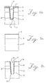
- the process starts by forming a patterned film 2 on a substrate 1, such as, for example, silicon, polysilicon, silicon dioxide, silicon nitride, conventional photoresists, etc.
- a substrate such as, for example, silicon, polysilicon, silicon dioxide, silicon nitride, conventional photoresists, etc.
- the film 2 is formed by exposing the substrate 1 through a mask (not shown) to a gaseous plasma which contains a compound that is strongly electron donating.
- the compound is a halogen-containing compound, preferably a fluorine-containing compound, and more preferably a fluorocarbon, such as trifluoromethane (CHF3).
- fluorocarbons for example, CF4, CF2C12, C4F8, etc., may be suitably employed.
- the plasma may include other compounds, such as oxygen or carbon dioxide, if it is desired, for example, to limit the thickness of the resulting film 2.
- the film 2 will form to a thickness ranging from about 1 - 100 nm (10 - 1000 ⁇ ), depending upon a number of factors, such as the composition of the plasma, the process conditions, such as pressure, power, time, etc., as should be apparent to those skilled in the art.
- the plasma treatment step is carried out in a conventional bell-jar type reactor system, such as an AME 8100, a commercial RIE system available from Applied Materials.
- the patterned film 2 may be formed by first forming a film over the substrate 1, and then patterning it in a conventional fashion.
- a suitable photolithographic material can be applied to the film and then patterned to expose selected areas of the film, followed by etching to transfer the pattern through the photolithographic material to form a pattern of openings in the film, such as shown in Fig. 1a. There again, the result is to expose selected areas of the substrate 1.
- the patterned film 2 and the exposed areas of the substrate 1 are then exposed to the vapor of a monomer, which is capable of condensing to form a conformal coating 3.
- the monomer comprises p-xylylene or a derivative thereof, and the vapor is produced by pyrolytic cleavage to produce divalent p-xylylene radicals which condense and polymerize on the exposed areas of the substrate 1 to form a homogeneous coating 3.
- the pyrolysis is generally carried out at a temperature greater than about 300 o C for a time which is sufficient to form a coating of desired thickness.
- the coating 3 has a thickness ranging from about 5 - 400 nm (50 - 4000 ⁇ ), and is prepared by employing a temperature from about 600 - 850 o C, at a pressure of about 4.000 - 133.32 Pa (30 - 1000 millitorr), for a time from about 0.5 - 45 minutes. More preferably, the coating 3 has a thickness ranging from about 100 - 300 nm (1000 - 3000 ⁇ ), with the time ranging from about 7-30 minutes.
- the resulting poly-p-xylylene polymers can be produced in a conventional apparatus which comprises a deposition chamber, in communication with a vaporization-pyrolysis furnace.
- the furnace is maintained at a temperature which is sufficiently high to cause evaporation and pyrolysis of the monomer to form the corresponding divalent radicals.
- These radicals pass to the deposition chamber and condense and polymerize upon contact with the surface of the substrate 1 to form a coating 3 comprising poly-p-xylylene or a derivative thereof.
- a conventional apparatus is shown, for example, in "Some Mechanical and Electrical Properties of Polyfluoro-p-Xylylene Films Prepared by Chemical Vapor Deposition," J. of Applied Polymer Science, Vol. 40, 1795-1800 (1990), the entire disclosure of which is incorporated herein by reference.
- Suitable p-xylylene monomers that can be employed in forming the polymer coatings in accordance with the process of the invention are disclosed, for example, in U.S. Pat. Nos. 3,342,754 and 3,900,600, the entire disclosures of both of which are incorporated herein by reference.
- the polymer does not substantially form on the patterned film 2.
- the nature of the film 2 is such that it inhibits substantial deposition of the coating, and this results in a selective deposition, so that the coating forms only on exposed areas of the substrate.
- the process of the invention provides a selective deposition of a conformal coating over patterned features of varying geometry.
- a conformal polymer coating is deposited on selected surfaces of a substrate trench.
- Examples 1a-5a a conventional vapor deposition system was used to deposit a coating of poly-p-xylylene.
- the substrate silicon wafer
- the vapor deposition chamber was placed in the vapor deposition chamber, and about 40-50 grams of p-xylylene were evaporated at 165 o C and 8.000 Pa (60 millitorr).
- the vapors were heated in a furnace at 800 o C to pyrolize the p-xylylene and form the corresponding divalent radicals.
- the radicals were then introduced into the deposition chamber, having a temperature of about 25-75 o C, where they condensed on the substrate surface to form a coating as summarized in Table I below.
- a film was first generated on a silicon wafer by exposing the wafer to a plasma mixture of trifluoromethane and carbon dioxide.
- the plasma polymerization was carried out in an AME 8100, a commercial RIE system made by Applied Materials, having a hexagonal-shaped electrode powered by 13.56 Mh rf power.
- the powered electrode was water cooled and covered with lexan or silicon fillers, the wafer being held to the electrode with four spring held clamps.
- the film was formed on the silicon surface according to the procedure outlined in Bariya, et al., Proceedings of the Seventh Symposium On Plasma Processing, The Electrochem. Soc., Proceedings Vol. 88-22 (1988), pp. 59-66, the entire disclosure of which is incorporated herein by reference. The following process conditions were employed:
- the film which formed on the silicon surface, can be characterized as a fluorinated polymer represented by the formula: (CF x ) y , where x is 1 to 3 and y is 1 to n, where n is an integer.
- the addition of the small amount of carbon dioxide caused a slight etching of the polymer, thus reducing the film thickness on the surface.
- Surface ESCA analysis showed the presence of a thin polymer film (3-5 nm), with CF, CF2 and CF3 bonding with minimal oxygen content.
- the film can be further characterized as stable and highly electron donating due to the presence of fluorine, which is strongly electronegative.
- fluorine-based (e.g., CF4, CF2Cl2, C4H8, etc.) monomer glow discharges should form polymers of similar composition and similar highly electron donating properties for selective deposition in accordance with the process of the present invention.
- Substrate Deposition time Thickness of Coating nm ( ⁇ ) 1a silicon 15 185.5 (1855) 1b film-coated silicon 15 0 (0) 2a silicon 30 294.2 (2942) 2b film-coated silicon 30 0 (0) 3a silicon 45 396.8 (3968) 3b film-coated silicon 45 5 (50) 4a silicon 60 516.9 (5169) 4b film-coated silicon 60 198.5 (1985) 5a silicon 75 762.4 (7624) 5b film-coated silicon 75 380.5 (3805)
- the purpose of the demonstration in the following examples was to determine the selectivity of deposition of a coating of poly-p-xylylene on trench substrate surfaces.
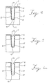
- trenches were formed in silicon substrates as follows: A p- epitaxial layer 4 was grown on a p+ substrate 5. A silicon oxide layer 6 was deposited on the epitaxial layer 4 using well known techniques (see Fig. 3a). A photoresist was then applied to the oxide layer 6, and after patterning, selected portions of the oxide layer 6 were removed to expose portions of the epitaxial layer 4. The oxide was etched in an AME 8100 etch tool, using a two-step process, viz.
- BCl3 (40 cm3/min at 0°C and 1013.3 hPa (sccm) gas flow, 1.333 Pa (10 millitorr) pressure and 950 watts of power), followed by 90 cm3/min at 0°C and 1013.3 hPa (sccm) HCl and 30 cm3/min at 0°C and 1013.3 hPa (sccm) Cl2 2.000 Pa (15 millitorr) pressure and 650 watts of power).
- a silicon oxychloride film 10 was formed on the sidewall surfaces 8, but not on the bottom surface 9, of the trench 7, as shown in Fig. 3b. It should be noted that this trench etch chemistry is particularly preferred, as it produces substantially vertical sidewall surfaces 8 and a rounded bottom surface 9.
- a trench 7 was first formed, following the procedure of Example 6. Then, a coating 11 of poly-p-xylylene 150 nm (1500 ⁇ ) was deposited over the silicon substrate, using the procedure of Examples 1-5. Poly-p-xylylene deposition occurred only on the horizontal substrate surfaces and on the bottom surface 9 of the trench 7. There was no deposition on the sidewalls 8 due to the formation of the silicon oxychloride film 10 during the trench etch, which inhibited deposition of poly-p-xylylene.
- a trench 7 was first formed, following the procedure of Example 6. Then, the oxychloride film 10 was removed from the trench sidewalls 8 by immersing the structure in a solution of buffered hydrofluoric acid. Next, the silicon substrate was exposed to a plasma mixture of trifluoromethane and carbon dioxide, using the procedure of Examples 1-5. This mixture did not etch the silicon surfaces, but did form a film 12 on all surfaces exposed to the plasma. Again following the procedure of Examples 1-5, the film was exposed to the vapor of p-xylylene, but there was no deposition of poly-p-xylylene on any surfaces, due to the presence of the film 12, which inhibited deposition.
- a trench 7 was first formed, following the procedure of Example 6. Then, the oxychloride film 10 was removed from the trench sidewalls 8 by immersing the structure in a solution of buffered hydrofluoric acid. Then, the silicon substrate was exposed to a plasma mixture of trifluoromethane and carbon dioxide, using the procedure of Examples 1-5. This mixture did not etch the silicon surfaces, but did form a film 12 on all surfaces exposed to the plasma.
- the film 12 was anisotropically etched in an AME 8100 etch tool with oxygen (30 cm3/min at 0°C and 1013.3 hPa (sccm) gas flow, 3.333 Pa (25 millitorr) pressure and 500 watts of power), so as to remove the film from the horizontal silicon surfaces, including the bottom surface 9 of the trench 7, but not from the vertical trench sidewalls 8, as shown in Fig. 6a.
- a coating 11 of poly-p-xylylene 150 nm (1500 ⁇ ) was deposited over the silicon substrate, using the procedure of Examples 1-5. There was no poly-p-xylylene deposition on the vertical trench sidewalls, but only on the horizontal surfaces, including the bottom surface 9 of the trench 7, as illustrated in Fig. 6b. There was no deposition on the sidewalls 8 due to the presence of the film 12, which inhibited deposition of poly-p-xylylene.
Landscapes
- Chemical Vapour Deposition (AREA)
- Formation Of Insulating Films (AREA)
Applications Claiming Priority (2)
| Application Number | Priority Date | Filing Date | Title |
|---|---|---|---|
| US678475 | 1991-04-01 | ||
| US07/678,475 US5618379A (en) | 1991-04-01 | 1991-04-01 | Selective deposition process |
Publications (2)
| Publication Number | Publication Date |
|---|---|
| EP0507183A2 true EP0507183A2 (de) | 1992-10-07 |
| EP0507183A3 EP0507183A3 (en) | 1993-10-20 |
Family
ID=24722934
Family Applications (1)
| Application Number | Title | Priority Date | Filing Date |
|---|---|---|---|
| EP19920105018 Withdrawn EP0507183A3 (en) | 1991-04-01 | 1992-03-24 | Process for selective deposition of a polymer coating |
Country Status (3)
| Country | Link |
|---|---|
| US (2) | US5618379A (de) |
| EP (1) | EP0507183A3 (de) |
| JP (1) | JPH07105387B2 (de) |
Cited By (2)
| Publication number | Priority date | Publication date | Assignee | Title |
|---|---|---|---|---|
| WO1999017892A1 (en) * | 1997-10-03 | 1999-04-15 | Massachusetts Institute Of Technology | Selective chemical vapor deposition of polymers |
| US6270872B1 (en) | 1998-05-19 | 2001-08-07 | Schering-Plough Healthcare Products, Inc. | Parylene coated devices with adhesive |
Families Citing this family (14)
| Publication number | Priority date | Publication date | Assignee | Title |
|---|---|---|---|---|
| DE19736370C2 (de) * | 1997-08-21 | 2001-12-06 | Bosch Gmbh Robert | Verfahren zum anisotropen Ätzen von Silizium |
| KR100358130B1 (ko) * | 1999-12-24 | 2002-10-25 | 주식회사 하이닉스반도체 | 트렌치 저면의 스트레스 집중 현상을 완화시킬 수 있는 트렌치형 소자분리막 형성방법 |
| US20010045527A1 (en) * | 2000-04-05 | 2001-11-29 | Wissman Barry Dean | Electron-beam cured polymer mask for DRIE micro-machining |
| US6737224B2 (en) * | 2001-04-17 | 2004-05-18 | Jeffrey Stewart | Method of preparing thin supported films by vacuum deposition |
| US20050007406A1 (en) * | 2001-04-19 | 2005-01-13 | Haas William S. | Controllable thermal warming devices |
| US7122296B2 (en) | 2002-03-05 | 2006-10-17 | Brewer Science Inc. | Lithography pattern shrink process and articles |
| US7064406B2 (en) * | 2003-09-03 | 2006-06-20 | Micron Technology, Inc. | Supression of dark current in a photosensor for imaging |
| DE102004028031A1 (de) * | 2004-06-09 | 2006-01-05 | Infineon Technologies Ag | Selektives Beschichtungsverfahren und Dünnschichtsystem |
| US7871933B2 (en) * | 2005-12-01 | 2011-01-18 | International Business Machines Corporation | Combined stepper and deposition tool |
| US8384183B2 (en) * | 2010-02-19 | 2013-02-26 | Allegro Microsystems, Inc. | Integrated hall effect element having a germanium hall plate |
| US8551877B2 (en) * | 2012-03-07 | 2013-10-08 | Tokyo Electron Limited | Sidewall and chamfer protection during hard mask removal for interconnect patterning |
| WO2017003791A1 (en) * | 2015-06-30 | 2017-01-05 | 3M Innovative Properties Company | Discontinuous coatings and methods of forming the same |
| JP6861535B2 (ja) * | 2017-02-28 | 2021-04-21 | 東京エレクトロン株式会社 | 処理方法及びプラズマ処理装置 |
| CN116351662B (zh) * | 2023-03-31 | 2024-05-17 | 浙江大学 | 一种聚合物薄膜区域选择性沉积的方法 |
Family Cites Families (16)
| Publication number | Priority date | Publication date | Assignee | Title |
|---|---|---|---|---|
| US3342754A (en) * | 1966-02-18 | 1967-09-19 | Union Carbide Corp | Para-xylylene polymers |
| US3895135A (en) * | 1973-05-01 | 1975-07-15 | Union Carbide Corp | Masking process with constricted flow path for coating |
| US3900600A (en) * | 1973-06-29 | 1975-08-19 | Ibm | Paraxylylene-silane dielectric films |
| US4163828A (en) * | 1978-01-20 | 1979-08-07 | Union Carbide Corporation | Parylene stabilization |
| US4299866A (en) * | 1979-07-31 | 1981-11-10 | International Business Machines Corporation | Coating process mask |
| US4636038A (en) * | 1983-07-09 | 1987-01-13 | Canon Kabushiki Kaisha | Electric circuit member and liquid crystal display device using said member |
| US4743327A (en) * | 1984-06-15 | 1988-05-10 | Cordis Corporation | Adhesive bonding of fluoropolymers |
| US4786675A (en) * | 1984-12-21 | 1988-11-22 | Nippon Zeon Co., Ltd. | Sealed semiconductor containing an epoxy resin composition |
| US4576834A (en) * | 1985-05-20 | 1986-03-18 | Ncr Corporation | Method for forming trench isolation structures |
| JPS6221151A (ja) * | 1985-07-19 | 1987-01-29 | Matsushita Electric Ind Co Ltd | パタ−ン形成方法 |
| IT1191646B (it) * | 1985-12-19 | 1988-03-23 | Montedison Spa | Processo per l'adesione di poli-p.xililene a substrati e articoli ottenuti |
| JPH0251226A (ja) * | 1988-08-12 | 1990-02-21 | Fuji Electric Co Ltd | 半導体装置の製造方法 |
| JPH02181428A (ja) * | 1989-01-06 | 1990-07-16 | Hitachi Ltd | 薄膜形成方法 |
| JPH02198153A (ja) * | 1989-01-27 | 1990-08-06 | Hitachi Ltd | 半導体装置の製造方法 |
| US4954609A (en) * | 1989-02-28 | 1990-09-04 | Hoechst Celanese Corp. | Intermediate molecular weight fluorine containing polymide and method for preparation |
| JP2753586B2 (ja) * | 1989-03-23 | 1998-05-20 | ティーディーケイ株式会社 | 高耐食性磁石 |
-
1991
- 1991-04-01 US US07/678,475 patent/US5618379A/en not_active Expired - Fee Related
-
1992
- 1992-02-15 JP JP4061297A patent/JPH07105387B2/ja not_active Expired - Lifetime
- 1992-03-24 EP EP19920105018 patent/EP0507183A3/en not_active Withdrawn
-
1996
- 1996-09-13 US US08/714,882 patent/US5714798A/en not_active Expired - Fee Related
Cited By (2)
| Publication number | Priority date | Publication date | Assignee | Title |
|---|---|---|---|---|
| WO1999017892A1 (en) * | 1997-10-03 | 1999-04-15 | Massachusetts Institute Of Technology | Selective chemical vapor deposition of polymers |
| US6270872B1 (en) | 1998-05-19 | 2001-08-07 | Schering-Plough Healthcare Products, Inc. | Parylene coated devices with adhesive |
Also Published As
| Publication number | Publication date |
|---|---|
| EP0507183A3 (en) | 1993-10-20 |
| JPH07105387B2 (ja) | 1995-11-13 |
| JPH06168935A (ja) | 1994-06-14 |
| US5714798A (en) | 1998-02-03 |
| US5618379A (en) | 1997-04-08 |
Similar Documents
| Publication | Publication Date | Title |
|---|---|---|
| EP0507183A2 (de) | Verfahren zur selektiven Ablagerung einer Schutzschicht aus Polymeren | |
| US6939808B2 (en) | Undoped and fluorinated amorphous carbon film as pattern mask for metal etch | |
| US6686295B2 (en) | Anisotropic etch method | |
| US4855017A (en) | Trench etch process for a single-wafer RIE dry etch reactor | |
| US5514247A (en) | Process for plasma etching of vias | |
| US9299581B2 (en) | Methods of dry stripping boron-carbon films | |
| US10510518B2 (en) | Methods of dry stripping boron-carbon films | |
| KR100880131B1 (ko) | 유기질 저유전율 재료의 에칭 방법 | |
| US5169487A (en) | Anisotropic etch method | |
| US6008139A (en) | Method of etching polycide structures | |
| KR20030022361A (ko) | 티타늄 질화물 에칭방법 | |
| US6428716B1 (en) | Method of etching using hydrofluorocarbon compounds | |
| US5549784A (en) | Method for etching silicon oxide films in a reactive ion etch system to prevent gate oxide damage | |
| US6372634B1 (en) | Plasma etch chemistry and method of improving etch control | |
| EP0820093A1 (de) | Ätzung einer organischen antireflektierenden Schicht von einem Substrat | |
| JP2004512673A (ja) | 炭素を含有するシリコン酸化物膜をエッチングする方法 | |
| US5271799A (en) | Anisotropic etch method | |
| Smolinsky et al. | Reactive ion etching of silicon oxides with ammonia and trifluoromethane. The role of nitrogen in the discharge | |
| US6455232B1 (en) | Method of reducing stop layer loss in a photoresist stripping process using a fluorine scavenger | |
| CN120769545A (zh) | 一种半导体工艺方法 | |
| KR960006171B1 (ko) | 폴리 실리콘 식각시 생성되는 클로로-카본 폴리머 제거방법 | |
| JPH05198538A (ja) | ドライエッチング方法 | |
| KR20050065740A (ko) | 반도체 소자의 트렌치 제조 방법 | |
| JPH06168913A (ja) | ドライエッチング方法 | |
| JPS6115156B2 (de) |
Legal Events
| Date | Code | Title | Description |
|---|---|---|---|
| PUAI | Public reference made under article 153(3) epc to a published international application that has entered the european phase |
Free format text: ORIGINAL CODE: 0009012 |
|
| AK | Designated contracting states |
Kind code of ref document: A2 Designated state(s): DE FR GB |
|
| PUAL | Search report despatched |
Free format text: ORIGINAL CODE: 0009013 |
|
| AK | Designated contracting states |
Kind code of ref document: A3 Designated state(s): DE FR GB |
|
| STAA | Information on the status of an ep patent application or granted ep patent |
Free format text: STATUS: THE APPLICATION IS DEEMED TO BE WITHDRAWN |
|
| 18D | Application deemed to be withdrawn |
Effective date: 19940901 |