EP0506175A2 - Flüssigkristallbildwiedergabeanordnung mit Orientierungsschicht - Google Patents
Flüssigkristallbildwiedergabeanordnung mit Orientierungsschicht Download PDFInfo
- Publication number
- EP0506175A2 EP0506175A2 EP92200757A EP92200757A EP0506175A2 EP 0506175 A2 EP0506175 A2 EP 0506175A2 EP 92200757 A EP92200757 A EP 92200757A EP 92200757 A EP92200757 A EP 92200757A EP 0506175 A2 EP0506175 A2 EP 0506175A2
- Authority
- EP
- European Patent Office
- Prior art keywords
- crystalline material
- orientation layer
- liquid
- display device
- crystal display
- Prior art date
- Legal status (The legal status is an assumption and is not a legal conclusion. Google has not performed a legal analysis and makes no representation as to the accuracy of the status listed.)
- Granted
Links
Images

Classifications
-
- G—PHYSICS
- G02—OPTICS
- G02F—OPTICAL DEVICES OR ARRANGEMENTS FOR THE CONTROL OF LIGHT BY MODIFICATION OF THE OPTICAL PROPERTIES OF THE MEDIA OF THE ELEMENTS INVOLVED THEREIN; NON-LINEAR OPTICS; FREQUENCY-CHANGING OF LIGHT; OPTICAL LOGIC ELEMENTS; OPTICAL ANALOGUE/DIGITAL CONVERTERS
- G02F1/00—Devices or arrangements for the control of the intensity, colour, phase, polarisation or direction of light arriving from an independent light source, e.g. switching, gating or modulating; Non-linear optics
- G02F1/01—Devices or arrangements for the control of the intensity, colour, phase, polarisation or direction of light arriving from an independent light source, e.g. switching, gating or modulating; Non-linear optics for the control of the intensity, phase, polarisation or colour
- G02F1/13—Devices or arrangements for the control of the intensity, colour, phase, polarisation or direction of light arriving from an independent light source, e.g. switching, gating or modulating; Non-linear optics for the control of the intensity, phase, polarisation or colour based on liquid crystals, e.g. single liquid crystal display cells
- G02F1/133—Constructional arrangements; Operation of liquid crystal cells; Circuit arrangements
- G02F1/1333—Constructional arrangements; Manufacturing methods
- G02F1/1337—Surface-induced orientation of the liquid crystal molecules, e.g. by alignment layers
- G02F1/133711—Surface-induced orientation of the liquid crystal molecules, e.g. by alignment layers by organic films, e.g. polymeric films
Definitions
- the invention relates to a method of manufacturing a liquid crystal display device comprising an orientation layer, said orientation layer being formed in contact with the surface of a mould, which mould is subsequently removed.
- the invention also relates to a liquid crystal display device comprising an orientation layer and switchable liquid-crystalline material.
- a liquid crystal display device comprises a cell with switchable liquid-crystalline material between two flat substrates on which electric conductor tracks may be present which can be used to switch the liquid-crystalline material between an "on” and an "off” state in accordance with a desired pattern.
- one or both substrates of a so-called active display device may additionally be provided with switching elements such as transistors.
- Orientation layers are frequently applied between a substrate having conductor tracks and the switchable liquid-crystalline material to provide the molecules of the liquid-crystalline material with a parallel (homogeneous), perpendicular (homeotropic) or oblique (tilted) preferred orientation. It is possible to provide an orientation layer on one or on both sides of the cell, i.e. on one or on both substrates.
- Polymer layers of, for example, polyethylene or polyimide are often used for this purpose, which layers are rubbed in one direction, for example, by means of a cloth.
- This has the disadvantage, however, that underlying electric elements such as wiring or transistors may be damaged, for example, mechanically or by a static charge.
- Another type of orientation layer consists of a layer of silicon oxide which is provided at an angle by vacuum evaporation, but such layers cannot readily be manufactured on a large scale.
- orientation layer for a liquid crystal display device is described in an abstract relating to the published Japanese Patent Application JP 1-94318, in Patent Abstracts of Japan, Volume 13, Number 329 (P-904) on page 122 (1989).
- the orientation layers are formed in contact with the surface of a mould which is subsequently removed.
- the surface of the mould contacting the orientation layers to be formed is provided with a saw-tooth structure which is transferred to the surface of the orientation layers.
- Said orientation layers which consist of polyimide, are rubbed in the desired directions after which the cell is filled with ferroelectric liquid-crystalline material and spacers in a manner which is known per se, and then sealed.
- a disadvantage of said known method resides in the necessity of using a mould having an accurately mechanically machined surface. Said method can only be used to obtain an orientation having a small angle of inclination. Further, an unsmooth intermediate face in the display device is undesirable because of the effects it has on the optical properties.
- the invention particularly aims at providing a method which can suitably be used for the manufacture of an active display device. It is an object of the invention to provide a liquid crystal display device comprising an orientation layer having a very effective orienting effect.
- the invention further aims at providing a display device having a flat and smooth orientation layer.
- the surface of the mould having an orienting effect consists of a rubbed polymer layer.
- Polymer layers which are customarily used for this purpose such as layers of polyethylene or polyimide, can suitably be used, which layers are rubbed in one direction, for example, with a non-fluff cotton cloth before they are used.
- the reactive liquid-crystalline material by means of actinic radiation.
- Actinic radiation is to be understood to mean herein, for example, radiation with UV light, electrons, X-rays, gamma rays or high-energy particles.
- the orientation layer is preferably cured by UV light in order to prevent the underlying electric elements from being damaged.
- UV light is used, in general, a small quantity of a light-sensitive initiator will be added to the reactive material according to a method which is known per se.
- the reactive liquid-crystalline material is cured, thereby forming a polymer network in which the non-reactive liquid-crystalline material is dispersed.
- a network can be manufactured by applying a monomer reactive material having at least two reactive groups per molecule.
- a stable material is obtained the properties of which are only slightly governed by, for example, temperature.
- a network it suffices to use a proportionately small quantity of reactive material relative to the quantity of non-reactive material.
- the choice of the non-reactive material enables the properties of the material of the orientation layer to be adapted to the requirements within wide limits.
- the object of providing a liquid crystal display device comprising an orientation layer and switchable liquid-crystalline material is achieved by a display device in which the orientation layer consists of an oriented polymer network in which a non-reactive liquid-crystalline material is dispersed.
- the orientation layer consists of an oriented polymer network in which a non-reactive liquid-crystalline material is dispersed.
- the invention can be used for the manufacture of a passive display device in which electric conductor tracks, for example of transparent indium oxide/tin oxide, may be situated on the substrate.
- the invention can very suitably be used for the manufacture of an active display device in which the orientation layer is provided on a substrate comprising electric switching elements.
- Such switching elements are constructed, in known manner, as semiconductor switches comprising, inter alia, transistors.
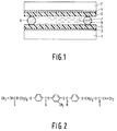
- a liquid crystal display device was manufactured from two flat substrates 1,2 of glass which were provided with electric conductor tracks 3,4 of indium oxide/tin oxide according to a desired pattern, see Fig. 1.
- the substrates may be provided with switching elements such as transistors which are constructed as, for example, thin layers of amorphous silicon.
- a mixture of liquid-crystalline materials was manufactured from 10% by weight of a reactive liquid-crystalline material, 88% by weight of a non-reactive liquid-crystalline material and 2% by weight of the light-sensitive initiator 2,2-dimethoxy-2-phenyl-aceto phenone.
- the diacrylate compound C6M the structural formula of which is shown in Fig. 2, was used as the reactive liquid-crystalline material.
- the mixture was provided on the substrates 1, 2 in the form of thin layers having a thickness of 10 ⁇ m and brought into contact with the surface of rubbed polyethylene foils. As a result thereof, the molecules of the mixture were oriented in the direction in which the foils were rubbed.
- the diacrylate compound C6M was made to cure by exposing it to UV light, thereby forming the orientation layers 5, 6.
- the intensity of the UV light was 0.2 mW/cm2 at the location of the layers 5, 6.
- a polymer network was formed in which the non-reactive material was dispersed. After curing the polyethylene foils were removed.
- a cell was manufactured by locating the substrates 1 and 2, including the layers provided thereon, opposite each other and providing a switchable liquid-crystalline material, according to the example the mixture E7, between said substrates. Glass fibres 8 having a diameter of 10 ⁇ m and serving as spacers were provided between the substrates.
- the cell was sealed in a customary manner by applying an epoxy resin adhesive, not shown in the Figure, along the edges of the cell.
- orientation layers 5 and 6 very effectively induce the desired orientation in the switchable liquid-crystalline material 7.
- the desired angle of inclination can be obtained within wide limits by adapting the composition of the orientation layers, in particular by the choice of the non-reactive liquid-crystalline material.
- the orientation layers have favourable optical properties such as transparency and flatness.
Landscapes
- Physics & Mathematics (AREA)
- Nonlinear Science (AREA)
- Spectroscopy & Molecular Physics (AREA)
- Mathematical Physics (AREA)
- Chemical & Material Sciences (AREA)
- Crystallography & Structural Chemistry (AREA)
- General Physics & Mathematics (AREA)
- Optics & Photonics (AREA)
- Liquid Crystal (AREA)
Applications Claiming Priority (2)
| Application Number | Priority Date | Filing Date | Title |
|---|---|---|---|
| EP91200676 | 1991-03-26 | ||
| EP91200676 | 1991-03-26 |
Publications (3)
| Publication Number | Publication Date |
|---|---|
| EP0506175A2 true EP0506175A2 (de) | 1992-09-30 |
| EP0506175A3 EP0506175A3 (en) | 1993-04-07 |
| EP0506175B1 EP0506175B1 (de) | 1996-12-04 |
Family
ID=8207570
Family Applications (1)
| Application Number | Title | Priority Date | Filing Date |
|---|---|---|---|
| EP92200757A Expired - Lifetime EP0506175B1 (de) | 1991-03-26 | 1992-03-17 | Flüssigkristallbildwiedergabeanordnung mit Orientierungsschicht |
Country Status (4)
| Country | Link |
|---|---|
| US (1) | US5262882A (de) |
| EP (1) | EP0506175B1 (de) |
| JP (1) | JP3121099B2 (de) |
| DE (1) | DE69215565T2 (de) |
Cited By (11)
| Publication number | Priority date | Publication date | Assignee | Title |
|---|---|---|---|---|
| EP0657763A3 (en) * | 1993-11-25 | 1995-06-28 | Sharp Kk | A liquid crystal display device. |
| EP0846976A1 (de) * | 1996-12-05 | 1998-06-10 | Samsung Display Devices Co., Ltd. | Flüssigkristallanzeige mit Orientierungsschichten aus einem polymerdispergierten Flüssigkristall und Verfahren zur Herstellung |
| WO1998049253A1 (en) * | 1997-04-29 | 1998-11-05 | Koninklijke Philips Electronics N.V. | Method of preparing a cross-linked macroscopically oriented polymer |
| US6201588B1 (en) | 1997-03-06 | 2001-03-13 | Sharp Kabushiki Kaisha | Liquid crystal optical element and liquid crystal device incorporating same |
| SG79925A1 (en) * | 1995-10-31 | 2001-04-17 | Rolic Ag | Liquid crystal cells for integrated optical components |
| WO2002044801A2 (en) | 2000-11-23 | 2002-06-06 | Merck Patent Gmbh | Homeotropic alignment layer |
| GB2388201A (en) * | 2002-04-30 | 2003-11-05 | Hewlett Packard Co | Liquid crystal device |
| WO2005008324A1 (en) * | 2003-07-18 | 2005-01-27 | Koninklijke Philips Electronics N.V. | Liquid crystal display device comprising an anchoring layer |
| CN100485492C (zh) * | 2004-02-10 | 2009-05-06 | 大日本印刷株式会社 | 液晶显示元件 |
| CN101952390A (zh) * | 2008-02-22 | 2011-01-19 | 株式会社艾迪科 | 含有聚合性化合物的液晶组合物和使用该液晶组合物的液晶显示元件 |
| CN103242863A (zh) * | 2013-04-19 | 2013-08-14 | 北京京东方光电科技有限公司 | 液晶复合材料、显示面板、显示装置及显示面板制造方法 |
Families Citing this family (29)
| Publication number | Priority date | Publication date | Assignee | Title |
|---|---|---|---|---|
| US5438421A (en) * | 1991-04-24 | 1995-08-01 | Alps Electric Co., Ltd. | Orientation film of liquid crystal having bilaterally asymmetric ridges separated by grooves |
| KR100231082B1 (ko) * | 1991-12-09 | 1999-11-15 | 요트. 게이.아. 롤페즈 | 액정 재료를 포함하는 표시 장치 및 그 제조방법 |
| US5473450A (en) * | 1992-04-28 | 1995-12-05 | Sharp Kabushiki Kaisha | Liquid crystal display device with a polymer between liquid crystal regions |
| JPH0647118A (ja) * | 1992-07-16 | 1994-02-22 | Tokyo Reinetsu Sangyo Kk | 水泳装置 |
| DE69306201T2 (de) * | 1992-09-01 | 1997-05-28 | Philips Electronics Nv | Einrichtung zur optischen Modulation |
| TW289095B (de) * | 1993-01-11 | 1996-10-21 | ||
| SG50569A1 (en) * | 1993-02-17 | 2001-02-20 | Rolic Ag | Optical component |
| JP2933816B2 (ja) * | 1993-07-15 | 1999-08-16 | シャープ株式会社 | 液晶表示素子及びその製造方法 |
| JP3102970B2 (ja) * | 1993-07-28 | 2000-10-23 | シャープ株式会社 | 情報表示装置およびその製造方法 |
| US5712696A (en) * | 1994-02-17 | 1998-01-27 | Stanley Electric, Co., Ltd. | Manufacture of LCD device by transferring the orientation state from a parent substrate to a child substrate |
| TW339415B (en) * | 1994-04-28 | 1998-09-01 | Chisso Corp | Processing and manufacturing method of LCD elements |
| JP3074111B2 (ja) * | 1994-05-27 | 2000-08-07 | シャープ株式会社 | 液晶パネル及びその製造方法 |
| JP3836140B2 (ja) * | 1995-02-28 | 2006-10-18 | コーニンクレッカ フィリップス エレクトロニクス エヌ ヴィ | 電気光学装置 |
| CN1163765C (zh) | 1997-05-09 | 2004-08-25 | 罗利克有限公司 | 光学元件和包含它的防伪或防拷贝元器件 |
| TW523621B (en) * | 1997-06-11 | 2003-03-11 | Koninkl Philips Electronics Nv | Multi-domain liquid-crystal display device |
| US6124970A (en) * | 1997-10-20 | 2000-09-26 | Latents Image Technology Ltd. | Polymer materials with latent images visible in polarized light and methods for their production |
| US5953091A (en) * | 1998-04-09 | 1999-09-14 | Ois Optical Imaging Systems, Inc. | Multi-domain LCD and method of making same |
| GB9812636D0 (en) * | 1998-06-11 | 1998-08-12 | Rolic Ag | Optical component orientation layer and layerable polymerisable mixture |
| AU3887100A (en) | 1999-11-12 | 2001-05-30 | 3M Innovative Properties Company | Liquid crystal alignment structure and display devices containing same |
| AU1763701A (en) | 1999-11-12 | 2001-06-06 | 3M Innovative Properties Company | Liquid crystal alignment structures and optical devices containing same |
| KR100542082B1 (ko) * | 1999-12-20 | 2006-01-10 | 엘지.필립스 엘시디 주식회사 | 액정 셀 제조방법 |
| US6699533B2 (en) | 2000-12-01 | 2004-03-02 | 3M Innovative Properties Company | Stabilized liquid crystal alignment structure with pre-tilt angle and display devices containing the same |
| US6791749B2 (en) * | 2001-08-29 | 2004-09-14 | Delpico Joseph | Polarized exposure for web manufacture |
| GB0209917D0 (en) * | 2002-04-30 | 2002-06-05 | Hewlett Packard Co | Bistable nematic liquid crystal device |
| TWI282009B (en) * | 2002-05-31 | 2007-06-01 | Sharp Kk | Liquid crystal display device and method of producing the same |
| WO2006123791A1 (ja) * | 2005-05-19 | 2006-11-23 | Dai Nippon Printing Co., Ltd. | 液晶表示素子および液晶表示素子の製造方法 |
| US7907247B2 (en) * | 2005-05-19 | 2011-03-15 | Dai Nippon Printing Co., Ltd. | Liquid crystal display |
| JP4839959B2 (ja) * | 2005-05-19 | 2011-12-21 | 大日本印刷株式会社 | 液晶表示素子 |
| TWI344032B (en) * | 2006-09-07 | 2011-06-21 | Taiwan Tft Lcd Ass | Liquid crystal display panel and method of fabricating the liquid crystal display panel |
Family Cites Families (10)
| Publication number | Priority date | Publication date | Assignee | Title |
|---|---|---|---|---|
| EP0157708B1 (de) * | 1984-04-05 | 1990-10-10 | Stein Heurtey | Entfettungsverfahren für kaltgewalztes Stahlband |
| DD252449A1 (de) * | 1986-09-04 | 1987-12-16 | Werk Fernsehelektronik Veb | Verfahren zur orientierung von fluessigkristallen |
| EP0261712A1 (de) * | 1986-09-04 | 1988-03-30 | Koninklijke Philips Electronics N.V. | Bildanzeigezelle, Verfahren zur Herstellung einer orientierenden Schicht über ein Substrat dieser Bildanzeigezelle und Monomer-Verbindung für ihre Anwendung als orientierende Schicht |
| JPH0194318A (ja) * | 1987-10-07 | 1989-04-13 | Matsushita Electric Ind Co Ltd | 液晶表示素子 |
| NL8802832A (nl) * | 1988-02-29 | 1989-09-18 | Philips Nv | Methode voor het vervaardigen van een gelaagd element en het aldus verkregen element. |
| US5067797A (en) * | 1988-03-25 | 1991-11-26 | Hitachi, Ltd. | Liquid crystal display cell and process for producing the same |
| JPH0328822A (ja) * | 1989-06-27 | 1991-02-07 | Nippon Oil Co Ltd | 液晶表示素子用補償板 |
| NL9001643A (nl) * | 1990-07-19 | 1992-02-17 | Philips Nv | Werkwijze voor het aanbrengen van een orientatielaag in een vloeibaar kristallijne beeldweergeefcel. |
| EP0501905A1 (de) * | 1991-02-27 | 1992-09-02 | Jordi Arnau Masdevall | Verpackung für Rollen aus befeuchtetem Papier für die Körperhygiene |
| EP0506176B1 (de) * | 1991-03-26 | 1996-02-07 | Koninklijke Philips Electronics N.V. | Lichtstreuelement |
-
1992
- 1992-03-17 DE DE69215565T patent/DE69215565T2/de not_active Expired - Fee Related
- 1992-03-17 EP EP92200757A patent/EP0506175B1/de not_active Expired - Lifetime
- 1992-03-23 JP JP04065278A patent/JP3121099B2/ja not_active Expired - Fee Related
- 1992-03-26 US US07/858,258 patent/US5262882A/en not_active Expired - Fee Related
Cited By (21)
| Publication number | Priority date | Publication date | Assignee | Title |
|---|---|---|---|---|
| EP0657763A3 (en) * | 1993-11-25 | 1995-06-28 | Sharp Kk | A liquid crystal display device. |
| US5512336A (en) * | 1993-11-25 | 1996-04-30 | Sharp Kabushiki Kaisha | Liquid crystal display device |
| SG79925A1 (en) * | 1995-10-31 | 2001-04-17 | Rolic Ag | Liquid crystal cells for integrated optical components |
| EP0846976A1 (de) * | 1996-12-05 | 1998-06-10 | Samsung Display Devices Co., Ltd. | Flüssigkristallanzeige mit Orientierungsschichten aus einem polymerdispergierten Flüssigkristall und Verfahren zur Herstellung |
| US5929957A (en) * | 1996-12-05 | 1999-07-27 | Samsung Display Devices Co., Ltd. | Liquid crystal display cell and method of making the same |
| US6201588B1 (en) | 1997-03-06 | 2001-03-13 | Sharp Kabushiki Kaisha | Liquid crystal optical element and liquid crystal device incorporating same |
| WO1998049253A1 (en) * | 1997-04-29 | 1998-11-05 | Koninklijke Philips Electronics N.V. | Method of preparing a cross-linked macroscopically oriented polymer |
| WO2002044801A2 (en) | 2000-11-23 | 2002-06-06 | Merck Patent Gmbh | Homeotropic alignment layer |
| WO2002044801A3 (en) * | 2000-11-23 | 2002-08-01 | Merck Patent Gmbh | Homeotropic alignment layer |
| US7105209B2 (en) | 2000-11-23 | 2006-09-12 | Merck Kgaa | Homeotropic alignment layer |
| GB2389191A (en) * | 2002-04-30 | 2003-12-03 | Hewlett Packard Development Co | Liquid crystal device |
| GB2389191B (en) * | 2002-04-30 | 2005-06-08 | Hewlett Packard Development Co | Liquid crystal device |
| GB2388201A (en) * | 2002-04-30 | 2003-11-05 | Hewlett Packard Co | Liquid crystal device |
| US7326449B2 (en) | 2002-04-30 | 2008-02-05 | Hewlett-Packard Development Company, L.P. | Liquid crystal device |
| WO2005008324A1 (en) * | 2003-07-18 | 2005-01-27 | Koninklijke Philips Electronics N.V. | Liquid crystal display device comprising an anchoring layer |
| CN100485492C (zh) * | 2004-02-10 | 2009-05-06 | 大日本印刷株式会社 | 液晶显示元件 |
| CN101364012B (zh) * | 2004-02-10 | 2010-09-22 | 大日本印刷株式会社 | 液晶显示元件 |
| CN101952390A (zh) * | 2008-02-22 | 2011-01-19 | 株式会社艾迪科 | 含有聚合性化合物的液晶组合物和使用该液晶组合物的液晶显示元件 |
| CN101952390B (zh) * | 2008-02-22 | 2013-10-16 | 株式会社艾迪科 | 含有聚合性化合物的液晶组合物和使用该液晶组合物的液晶显示元件 |
| CN103242863A (zh) * | 2013-04-19 | 2013-08-14 | 北京京东方光电科技有限公司 | 液晶复合材料、显示面板、显示装置及显示面板制造方法 |
| CN103242863B (zh) * | 2013-04-19 | 2015-07-29 | 北京京东方光电科技有限公司 | 液晶复合材料、显示面板、显示装置及显示面板制造方法 |
Also Published As
| Publication number | Publication date |
|---|---|
| DE69215565T2 (de) | 1997-05-28 |
| EP0506175B1 (de) | 1996-12-04 |
| DE69215565D1 (de) | 1997-01-16 |
| US5262882A (en) | 1993-11-16 |
| JPH0580341A (ja) | 1993-04-02 |
| EP0506175A3 (en) | 1993-04-07 |
| JP3121099B2 (ja) | 2000-12-25 |
Similar Documents
| Publication | Publication Date | Title |
|---|---|---|
| EP0506175B1 (de) | Flüssigkristallbildwiedergabeanordnung mit Orientierungsschicht | |
| EP0552508B1 (de) | Anzeigevorrichtung mit Flüssigkristallmaterial | |
| US5570216A (en) | Bistable cholesteric liquid crystal displays with very high contrast and excellent mechanical stability | |
| JP3070777B2 (ja) | 液晶材料およびこれを使用する表示セル | |
| US5365356A (en) | Method of fabricating an encapsulated liquid crystal display | |
| JP2669609B2 (ja) | 液晶表示素子 | |
| JPH04220620A (ja) | 液晶電気光学装置の作製方法 | |
| CN1239232A (zh) | 液晶电光显示装置及其制造方法 | |
| EP0733228B1 (de) | Anzeigevorrichtung | |
| EP0420670B1 (de) | Orientierungsfilm für Flüssigkristall und sein Herstellungsverfahren und Flüssigkristallelement mit diesem Film | |
| JPH0369921A (ja) | 電気導電性高分子及び電気導電性高分子を用いた液晶スイッチ及びディスプレー素子における配向層 | |
| US3966304A (en) | Liquid crystal display device | |
| JPH04240614A (ja) | 液晶電気光学素子 | |
| JPH0720479A (ja) | 液晶素子およびその製造方法 | |
| US7834963B2 (en) | Optical integrator | |
| EP0540806A2 (de) | Flüssigkristallfilm | |
| EP0224328A1 (de) | Optische Vorrichtungen mit ferroelektrischen Flüssigkristallen | |
| JPS63136024A (ja) | 液晶配向膜およびその製造法 | |
| JPH03102323A (ja) | 液晶パネル及びその製造方法 | |
| Wilson et al. | Alignment of liquid crystals on surfaces with films deposited obliquely at low and high rates | |
| Ji et al. | The mechanism for the formation of polymer wall in higher polymer content cholesteric liquid crystal mixture | |
| JPS55157719A (en) | Liquid crystal display panel | |
| KR950004383B1 (ko) | 고분자 분산 네마틱 액정 표시 소자와 그 구동 방법 | |
| JP3027523B2 (ja) | 液晶用配向膜の形成方法 | |
| JPH05257152A (ja) | 液晶表示素子 |
Legal Events
| Date | Code | Title | Description |
|---|---|---|---|
| PUAI | Public reference made under article 153(3) epc to a published international application that has entered the european phase |
Free format text: ORIGINAL CODE: 0009012 |
|
| AK | Designated contracting states |
Kind code of ref document: A2 Designated state(s): DE FR GB |
|
| PUAL | Search report despatched |
Free format text: ORIGINAL CODE: 0009013 |
|
| AK | Designated contracting states |
Kind code of ref document: A3 Designated state(s): DE FR GB |
|
| 17P | Request for examination filed |
Effective date: 19931005 |
|
| 17Q | First examination report despatched |
Effective date: 19950523 |
|
| GRAG | Despatch of communication of intention to grant |
Free format text: ORIGINAL CODE: EPIDOS AGRA |
|
| GRAH | Despatch of communication of intention to grant a patent |
Free format text: ORIGINAL CODE: EPIDOS IGRA |
|
| GRAH | Despatch of communication of intention to grant a patent |
Free format text: ORIGINAL CODE: EPIDOS IGRA |
|
| GRAA | (expected) grant |
Free format text: ORIGINAL CODE: 0009210 |
|
| AK | Designated contracting states |
Kind code of ref document: B1 Designated state(s): DE FR GB |
|
| REF | Corresponds to: |
Ref document number: 69215565 Country of ref document: DE Date of ref document: 19970116 |
|
| ET | Fr: translation filed | ||
| PLBE | No opposition filed within time limit |
Free format text: ORIGINAL CODE: 0009261 |
|
| STAA | Information on the status of an ep patent application or granted ep patent |
Free format text: STATUS: NO OPPOSITION FILED WITHIN TIME LIMIT |
|
| 26N | No opposition filed | ||
| REG | Reference to a national code |
Ref country code: FR Ref legal event code: CD |
|
| REG | Reference to a national code |
Ref country code: GB Ref legal event code: IF02 |
|
| REG | Reference to a national code |
Ref country code: GB Ref legal event code: 746 Effective date: 20021017 |
|
| REG | Reference to a national code |
Ref country code: FR Ref legal event code: D6 |
|
| PGFP | Annual fee paid to national office [announced via postgrant information from national office to epo] |
Ref country code: FR Payment date: 20030328 Year of fee payment: 12 |
|
| PGFP | Annual fee paid to national office [announced via postgrant information from national office to epo] |
Ref country code: GB Payment date: 20030331 Year of fee payment: 12 |
|
| PGFP | Annual fee paid to national office [announced via postgrant information from national office to epo] |
Ref country code: DE Payment date: 20030515 Year of fee payment: 12 |
|
| PG25 | Lapsed in a contracting state [announced via postgrant information from national office to epo] |
Ref country code: GB Free format text: LAPSE BECAUSE OF NON-PAYMENT OF DUE FEES Effective date: 20040317 |
|
| PG25 | Lapsed in a contracting state [announced via postgrant information from national office to epo] |
Ref country code: DE Free format text: LAPSE BECAUSE OF NON-PAYMENT OF DUE FEES Effective date: 20041001 |
|
| GBPC | Gb: european patent ceased through non-payment of renewal fee |
Effective date: 20040317 |
|
| PG25 | Lapsed in a contracting state [announced via postgrant information from national office to epo] |
Ref country code: FR Free format text: LAPSE BECAUSE OF NON-PAYMENT OF DUE FEES Effective date: 20041130 |
|
| REG | Reference to a national code |
Ref country code: FR Ref legal event code: ST |