EP0502739B1 - System zur Rückgewinnung von Daten und NRZ-Taktsignalen mit einer Phasenregelschleife - Google Patents
System zur Rückgewinnung von Daten und NRZ-Taktsignalen mit einer Phasenregelschleife Download PDFInfo
- Publication number
- EP0502739B1 EP0502739B1 EP92301912A EP92301912A EP0502739B1 EP 0502739 B1 EP0502739 B1 EP 0502739B1 EP 92301912 A EP92301912 A EP 92301912A EP 92301912 A EP92301912 A EP 92301912A EP 0502739 B1 EP0502739 B1 EP 0502739B1
- Authority
- EP
- European Patent Office
- Prior art keywords
- signal
- nrz
- blivet
- produce
- clock
- Prior art date
- Legal status (The legal status is an assumption and is not a legal conclusion. Google has not performed a legal analysis and makes no representation as to the accuracy of the status listed.)
- Expired - Lifetime
Links
Images


Classifications
-
- H—ELECTRICITY
- H03—ELECTRONIC CIRCUITRY
- H03L—AUTOMATIC CONTROL, STARTING, SYNCHRONISATION OR STABILISATION OF GENERATORS OF ELECTRONIC OSCILLATIONS OR PULSES
- H03L7/00—Automatic control of frequency or phase; Synchronisation
- H03L7/06—Automatic control of frequency or phase; Synchronisation using a reference signal applied to a frequency- or phase-locked loop
- H03L7/08—Details of the phase-locked loop
- H03L7/085—Details of the phase-locked loop concerning mainly the frequency- or phase-detection arrangement including the filtering or amplification of its output signal
- H03L7/089—Details of the phase-locked loop concerning mainly the frequency- or phase-detection arrangement including the filtering or amplification of its output signal the phase or frequency detector generating up-down pulses
-
- G—PHYSICS
- G11—INFORMATION STORAGE
- G11B—INFORMATION STORAGE BASED ON RELATIVE MOVEMENT BETWEEN RECORD CARRIER AND TRANSDUCER
- G11B20/00—Signal processing not specific to the method of recording or reproducing; Circuits therefor
- G11B20/10—Digital recording or reproducing
- G11B20/14—Digital recording or reproducing using self-clocking codes
- G11B20/1403—Digital recording or reproducing using self-clocking codes characterised by the use of two levels
- G11B20/1407—Digital recording or reproducing using self-clocking codes characterised by the use of two levels code representation depending on a single bit, i.e. where a one is always represented by a first code symbol while a zero is always represented by a second code symbol
- G11B20/1419—Digital recording or reproducing using self-clocking codes characterised by the use of two levels code representation depending on a single bit, i.e. where a one is always represented by a first code symbol while a zero is always represented by a second code symbol to or from biphase level coding, i.e. to or from codes where a one is coded as a transition from a high to a low level during the middle of a bit cell and a zero is encoded as a transition from a low to a high level during the middle of a bit cell or vice versa, e.g. split phase code, Manchester code conversion to or from biphase space or mark coding, i.e. to or from codes where there is a transition at the beginning of every bit cell and a one has no second transition and a zero has a second transition one half of a bit period later or vice versa, e.g. double frequency code, FM code
-
- H—ELECTRICITY
- H03—ELECTRONIC CIRCUITRY
- H03L—AUTOMATIC CONTROL, STARTING, SYNCHRONISATION OR STABILISATION OF GENERATORS OF ELECTRONIC OSCILLATIONS OR PULSES
- H03L7/00—Automatic control of frequency or phase; Synchronisation
- H03L7/06—Automatic control of frequency or phase; Synchronisation using a reference signal applied to a frequency- or phase-locked loop
- H03L7/08—Details of the phase-locked loop
- H03L7/085—Details of the phase-locked loop concerning mainly the frequency- or phase-detection arrangement including the filtering or amplification of its output signal
- H03L7/087—Details of the phase-locked loop concerning mainly the frequency- or phase-detection arrangement including the filtering or amplification of its output signal using at least two phase detectors or a frequency and phase detector in the loop
-
- H—ELECTRICITY
- H03—ELECTRONIC CIRCUITRY
- H03M—CODING; DECODING; CODE CONVERSION IN GENERAL
- H03M5/00—Conversion of the form of the representation of individual digits
- H03M5/02—Conversion to or from representation by pulses
- H03M5/04—Conversion to or from representation by pulses the pulses having two levels
- H03M5/14—Code representation, e.g. transition, for a given bit cell depending on the information in one or more adjacent bit cells, e.g. delay modulation code, double density code
-
- H—ELECTRICITY
- H04—ELECTRIC COMMUNICATION TECHNIQUE
- H04L—TRANSMISSION OF DIGITAL INFORMATION, e.g. TELEGRAPHIC COMMUNICATION
- H04L7/00—Arrangements for synchronising receiver with transmitter
- H04L7/0079—Receiver details
- H04L7/0087—Preprocessing of received signal for synchronisation, e.g. by code conversion, pulse generation or edge detection
-
- H—ELECTRICITY
- H04—ELECTRIC COMMUNICATION TECHNIQUE
- H04L—TRANSMISSION OF DIGITAL INFORMATION, e.g. TELEGRAPHIC COMMUNICATION
- H04L7/00—Arrangements for synchronising receiver with transmitter
- H04L7/02—Speed or phase control by the received code signals, the signals containing no special synchronisation information
- H04L7/033—Speed or phase control by the received code signals, the signals containing no special synchronisation information using the transitions of the received signal to control the phase of the synchronising-signal-generating means, e.g. using a phase-locked loop
-
- Y—GENERAL TAGGING OF NEW TECHNOLOGICAL DEVELOPMENTS; GENERAL TAGGING OF CROSS-SECTIONAL TECHNOLOGIES SPANNING OVER SEVERAL SECTIONS OF THE IPC; TECHNICAL SUBJECTS COVERED BY FORMER USPC CROSS-REFERENCE ART COLLECTIONS [XRACs] AND DIGESTS
- Y10—TECHNICAL SUBJECTS COVERED BY FORMER USPC
- Y10S—TECHNICAL SUBJECTS COVERED BY FORMER USPC CROSS-REFERENCE ART COLLECTIONS [XRACs] AND DIGESTS
- Y10S331/00—Oscillators
- Y10S331/02—Phase locked loop having lock indicating or detecting means
Definitions
- This invention relates to digital data transmission, and more particularly to non-return to zero (NRZ) clock and data recovery.
- NRZ non-return to zero
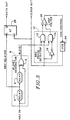
- FIG. 1 shows one prior art approach to this problem.
- a non-linearity in the form of a delay line and an exclusive-OR gate, is introduced to produce a frequency component at the NRZ clock frequency.
- the delay element is typically one half of the expected bit interval or less.
- a bandpass filter detects the introduced frequency component at the clock frequency and either produces a clock directly or produces a clock indirectly with the assistance of a phase lock loop.
- FIG. 2 Another prior art approach is shown in FIG. 2. This approach does not require a tuned circuit and is therefore more amenable to IC implementation.
- the accuracy of the placement of the clock edge in the center of the bit interval depends primarily on the length of the delay line. In all of the typical IC implementations of a delay line, the amount of delay that results is subject to process and temperature variations. Thus, the clock edge is not well centered within the bit interval and, in the presence of significant jitter, the bit error rate suffers accordingly.
- US-A-4590602, US-A-3992581 and EP-A-0009939 disclose input processing circuits for producing a pulse at each transition of an input signal, which pulses are input to a phase detector for comparison with a VCO output clock signal.
- the phase compared signal is filtered to provide a control signal to the VCO so that the VCO provides the recovered clock signal.
- the recovered clock is applied to a data flip-flop to which also is applied the input signal to provide the data output.
- US-A-4590602 also shows a frequency detector that compares a reference frequency from a separate oscillator with a sub-divided version of the VCO frequency (recovered clock) to provide an input to a summation circuit to which is also input the output of the phase detector, the sum being input to a loop filter.
- the frequency detector is inhibited by a lock detector that has the recovered clock and pulsed signal at each transition of the input signal, as inputs.
- NRZ data is applied to one side of an exclusive-OR gate and a twice delayed version of the NRZ data is applied to the other side.
- the output of the XOR gate a "blivet" signal, is applied to a NRZ phase detector comprising two AND gates, one of which has as its other input a recovered clock signal output of a VCO and the other of which has as its other input an inverted version of the recovered clock signal.
- the outputs of the two AND gates are an "up” signal and a "down” signal that indicate which direction a frequency control signal should change the VCO frequency.
- a data holding flip-flop whose input is a once delayed version of the NRZ data is clocked with the recovered clock signal.
- an NRZ frequency detector that includes two flip-flops for monitoring the state of the recovered clock signal on opposite edges of the blivet signal.
- Three gates monitor the output of the two flip-flops to detect too-high, too-low and "good” conditions. Additional flip-flops hold the results of this detection, and feedback from these flip-flops is used to inhibit detection of error states that are the opposite of an immediately preceding error state.
- the flip-flops holding the results of the detection can be forced to ignore their inputs and hold a "good” instead if a lock signal indicates that the phase lock loop is locked.
- a lock detector consisting of a saturating up/down counter that is incremented by one when blivets occur and the NRZ frequency detector is signaling a "good” condition and is decremented by a number larger than one when blivets occur and the NRZ frequency detector is signaling "not-good".
- a lock signal output is produced whenever the count in the counter is above a predetermined threshold, e.g. half full.
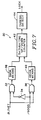
- FIG. 3 is a block diagram of a portion of the NRZ clock and data recovery circuit according to the present invention, with an inset schematic detail of the phase detection circuitry 10. This design lends itself to integration and provides automatic centering of the clock edge within the bit interval in a manner that is independent of analog delays and process and temperature variations.
- the NRZ data input is applied to a unique "blivet” generator 8.
- a "blivet” is a pulse indicative of a transition, either low-going or high-going, in the NRZ data.
- the NRZ data input is applied to one side of exclusive-OR (XOR) gate 6 and also to two matching delay elements 2 and 4 in series, after which the doubly delayed output of those delay elements is applied to the other side of the XOR gate 6.
- blivet generator 8 also provides an NRZ output that is delayed by one half of the blivet width.
- the blivet output of the blivet generator is a pulse whose duration is the sum of the delay imposed by the two matching delay elements 2 and 4. As will be further explained below, the sum of these delays should be less than one half of the bit interval of the expected data, but as long as possible within that constraint.
- the blivet output of the blivet generator 8, from XOR gate 6, is applied to NRZ phase detector 10, which also receives a clock output from a VCO 20.
- the NRZ phase detector 10 comprises AND gates 12 and 14 and inverter 16.
- the NRZ phase detector 10 generates two signals, an "up” signal that goes to the "+” input of loop filter 26, and a “down” signal that goes to the "-" input of the loop filter 26.
- the “up” and “down” signals are used by the loop filter 26 to produce the control voltage for VCO 20.
- the loop filter 26, which is suitably a charge pump, receives the "up” and “down” pulses from the NRZ phase detector 10 and integrates their difference into an analog VCO control signal with only low frequency components.
- the effectiveness of this invention relies on the centering of the low-going edge of the VCO 20 recovered clock output within this blivet.
- the duration of the output from AND gate 12 is the same as the duration of the output from AND gate 14, and the inputs to the loop filter 26 cancel, indicating that no frequency adjustment is necessary and the loop filter 26 continues to produce an unchanged VCO control signal.
- the output of AND gate 12 has a longer duration than the output of AND gate 14, and the "up" input to the loop filter prevails over the "down” input and the VCO control voltage output of the loop filter 26 increases the VCO frequency to cause the next low-going edge to occur sooner within the blivet interval.
- the NRZ phase detector 10 and loop filter 26 operate over time to force the downward edge of the clock signal from VCO 20 to the center of the blivet interval.
- the delay elements 2 and 4 are identical, they produce equal delays despite process and temperature variations. Therefore, changes in process or temperature affect the blivet width, which affects the NRZ phase detector's sensitivity, but not its ability to properly detect phase differences. Sensitivity increases with increasing blivet width, because the difference between the widths of the "up" and “down" pulses can be greater.
- the clock output of the VCO 20 is also applied to the clock input of flip-flop 28.
- the D input of flip-flop 28 is connected to receive the once delayed NRZ data output of the blivet generator 8, from the output of delay element 2.
- the ability to position the clock edge that clocks the data into flip-flop 28 in the center of the "eye" of the bit interval depends on the centering of the opposite clock edge within the blivet, as described above.
- the VCO is balanced to have a near perfect 50% duty cycle. So, with the VCO 20 clock output low-going transitions centered in the blivets from XOR gate 6, the high going transitions are guaranteed to occur while the data present at the junction of the two delay elements 2 and 4 is right in the middle of the bit interval. This is because the falling clock edge occurred half of blivet after the end of the last bit interval, and data at this junction is also delayed by one half blivet at the time of the rising clock edge.
- the D input of flip-flop 28 is connected to this junction between the delay elements 2 and 4 and is clocked by the rising edge of the VCO 20 output clock signals.
- the circuit shown in FIG. 3 reliably recovers NRZ clock and data signals and lends itself to integration into an IC.
- a complete system for NRZ clock and data recovery includes all of the circuitry shown in FIG. 3, plus an NRZ frequency detector 50, a lock detector 30 and OR gates 24 and 22 for combining the "up" and “down” outputs of the phase and NRZ frequency detectors before they are presented to the loop filter 26.
- the blivet signal is supplied to the NRZ frequency detector 50 and the lock detector 30, as well as the NRZ phase detector 10.
- the NRZ frequency detector 50 also receives the clock output of the VCO 20 and a "lock" signal from the lock detector 30.
- the NRZ frequency detector 50 produces “up” and “down” signals to steer the VCO 20 via the loop filter 26. These "up” and “down” signals are combined with the "up” and “down” signals from the NRZ phase detector 10 by up OR gate 24 and down OR gate 22.
- the NRZ frequency detector 50 also produces "not-good” signals that inform the lock detector 30 when the present blivet is going to cause an "up” or "down” signal.
- the NRZ frequency detector 50 contains four flip-flops 52, 57, 58 and 59 that are clocked by the rising edge of the blivet signal and one flip-flop 53 that is clocked by the falling edge of the blivet signal, due to the operation of inverter 51.
- Flip-flops 52 and 53 monitor the clock output of the VCO 20 on opposite edges of the blivet signal.
- a "good" blivet is a blivet whose rising edge occurs while the VCO 20 clock out is high and whose falling edge occurs while it is low.
- a good blivet therefore sets flip-flop 52 and resets flip-flop 53.
- NAND gate 54 monitors the Q output of flip-flop 52 and the /Q output of flip-flop 53, and produces a low output whenever a good blivet has been detected by these two flip-flops.
- NAND gate 55 monitors the states of flip-flops 52 and 53 for the "tool-low” condition, i.e., both flip-flops having a high output.
- the third input to this NAND gate 55 is from the D-C flip-flop created by NAND gates 62 and 63, which produces a high output from NAND gate 62 and a low output from NAND gate 63 when the frequency is too high.
- the reason for this third input to NAND gate 55 is to prevent going directly from a "too-high” condition to a "too-low” condition without going through a good state in-between.
- NAND gate 55 is prevented from producing an active-low output indicating that the next state should be “Up (too-low)” by the low output of NAND gate 63.
- NAND gate 56 monitors the states of flip-flops 52 and 53 for the "too-high” condition, i.e., both flip-flops having a low output. And, in the same way as before, a high output of NAND gate 61 in the other D-C flip-flop, indicating that the last state was not "too-low", is required before an active "too-high" signal can be produced.
- the D-C flip-flops 64 and 65 comprising NAND gates 60, 61 and 62, 63 hold the last known frequency direction, too-low, too-high or neither, until a /good blivet occurs.
- An active low/good signal attempts to clear both of the D-C flip-flops, and will do so in the absence of an active low /too-low or /too-high signal.
- the states of the NAND gates 54, 55 and 56 are clocked into flip-flops 57, 58 and 59, respectively, by the rising edge of the next blivet, if the signal lock is inactive low, indicating that the phase lock loop is not locked. If the signal lock is active high, indicating that a phase lock loop lock has been detected, the signal lock forces the /good flip-flop 57 to its cleared state, producing an inactive high output from that flip-flip, which indicates that the state is "good”. The active high lock signal also forces the "too-low” and "too-high” flip-flops to ignore their inputs from NAND gates 55 and 56, respectively, and produce inactive high outputs. Thus, while the loop is locked, the NRZ frequency detector cannot produce any output to disrupt that lock, leaving control entirely up to the NRZ phase detector 10.
- the lock detector 30 can respond by decrementing down to below its one half full level and going to an unlocked condition.
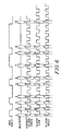
- FIG. 6 a series of blivets produces appropriate results in the presence of three different clock frequencies, one correct, one too-high and one too-low.
- good relationships between blivets and clock levels are indicated by “O"s above clock signal, while too low relationships are indicated with an “L” and too-highs with an “H”.
- the good blivet at blivet 8 is detected by NAND gate 54, whose output goes low in response.
- the good state of flip-flops 52 and 53 also means that neither of the other NAND gates 55 or 56 are satisfied.
- the low output of NAND gate 54 is clocked into flip-flop 57 on the rising edge of blivet 9.
- the same rising clock edge of blivet 9 also clocks the high levels that are present on the output of NAND gates 55 and 56 into flip-flops 58 and 59, respectively.
- the low output of flip-flop 57 immediately clears the two D-C flip-flops 60,61 and 62,63, so that their outputs on NAND gates 60 and 62 become low, since both of both of their inputs are now high.
- the cleared states of the D-C flip-flops 60,61 and 62,63 enable the third inputs to NAND gates 55 and 56, allowing them tc detect the next high or low state. If the frequency were now correct, mostly good blivets would be detected from now on and the NRZ frequency detector would behave as it does on the line labeled "Correct Clock Freq".
- the blivet length has to be less than one half of the bit interval.
- resistors implemented in silicon and metal capacitors both have tolerances of up to +/- 20%, and the delay elements 2 and 4 are based on an RC product of such devices, the worst case delay tolerance could be as bad as +/- 40%.
- the worst case deviation still leaves the resulting total delay under half of the bit interval, thereby permitting the NRZ frequency detector 50 to function properly.
- Counter 42 is a saturating up/down counter.
- a saturating counter is a counter that does not wrap around; when it reaches a full count, it stays there as additional increment signals are received.
- the saturating up/down counter 42 is incremented by incrementing means 38 whenever a "good" blivet is detected by AND gate 32, and decremented by decrementing means 40 whenever a "bad" blivet is detected by AND gate 36.
- Inverter 34 changes the /good signal into a good signal for AND gate 32. When the count in the counter reaches a threshold, for instance, more than half full, a "lock" signal is generated.
- the ratio of the increment step size (typically one) to the decrement step size (typically some multiple of increment size) determines the tolerance of the lock detector 30 to jitter.
- a 1:4 ratio has been found to provide a suitable jitter tolerance.
- the size of the saturating up/down counter 42 (in bits) determines the integration time of the lock detector 30, and hence its response time to a locked or unlocked condition. There is a trade-off between the speed with which a lock is identified and the certainty of that identification. In the present application, 12 bits of binary, for a total count of 4096, has been found to be a suitable length for this counter, so that a lock indication appears after a count of 2048. If jitter is minimal, a lock is achieved in about 15 microseconds at 270 Megabits per second.
- This lock detector 30 implementation is completely digital and therefore does not require an analog integration capacitor and associated IC pin. This is a significant benefit in some applications where a shortage of IC pins is an important design constraint.
- the present invention provides an improved NRZ clock and data recovery system that lends itself to integration, that includes a NRZ phase detector, preferably an NRZ frequency detector and a lock detector, preferably and that provides automatic centering of the clock edge within the bit interval in a manner that is independent of analog delays and process and temperature variations.
Landscapes
- Engineering & Computer Science (AREA)
- Signal Processing (AREA)
- Computer Networks & Wireless Communication (AREA)
- Theoretical Computer Science (AREA)
- Synchronisation In Digital Transmission Systems (AREA)
- Stabilization Of Oscillater, Synchronisation, Frequency Synthesizers (AREA)
- Dc Digital Transmission (AREA)
Claims (9)
- System zur Rückgewinnung von Daten und NRZ-Taktsignalen unter Verwendung einer Phasenregelschleife, gekennzeichnet durch:einen Blivet-Generator (8), der so gekoppelt ist, daß er ein NRZ-Eingangssignal empfängt, um ein einfach verzögertes NRZ-Signal zu erzeugen sowie ein Blivet-Signal, das von einem zweifach verzögerten NRZ-Signal und dem NRZ-Eingangssignal abgeleitet wird, wobei das Blivet-Signal einen Impuls für jeden Übergang des NRZ-Eingangssignals vorsieht;einen steuerbaren Oszillator (20), der so gekoppelt ist, daß er ein Oszillator-Steuersignal empfängt, um ein wiedergewonnenes Taktsignal zu erzeugen;einen NRZ-Phasendetektor (10), der so gekoppelt ist, daß er das wiedergewonnene Taktsignal und das Blivet-Signal empfängt, um ein erstes Aufwärtssignal sowie ein erstes Abwärtssignal zu erzeugen;einen Schleifenfilter (26), der so gekoppelt ist, daß er als erste und zweite Eingaben das erste Aufwärts- und das erste Abwärtssignal empfängt, um das Oszillator-Steuersignal zu erzeugen; undeine Datenrückgewinnungsschaltung (28), die so gekoppelt ist, daß sie das einfach verzögerte NRZ-Signal empfängt, um als Reaktion auf das wiedergewonnene Taktsignal ein Datenrückgewinnungs-Ausgangssignal zu erzeugen.
- System zur Rückgewinnung von Daten und NRZ-Taktsignalen nach Anspruch 1, wobei das System ferner folgendes umfaßt:einen Frequenzdetektor (50), der so gekoppelt ist, daß er das Blivet-Signal und das wiedergewonnene Taktsignal empfängt, um ein zweites Aufwärtssignal und ein zweites Abwärtssignal zu erzeugen; undeine Kombinationsschaltung (22, 24), die zwischen den NRZ-Phasendetektor und den Schleifenfilter gekoppelt ist, um die ersten und zweiten Aufwärts- und Abwärtssignale zu empfangen, um ein kombiniertes Aufwärtssignal und ein kombiniertes Abwärtssignal als erste und zweite Eingaben in den Schleifenfilter zu erzeugen.
- System zur Rückgewinnung von Daten und NRZ-Taktsignalen nach Anspruch 2, wobei das System ferner einen Sperrdetektor (30) umfaßt, der so gekoppelt ist, daß er das Blivet-Signal und ein Negations-Blivet-Signal von dem Fequenzdetektor empfängt, um ein Sperrsignal zu erzeugen, um den Frequenzdetektor daran zu hindern, daß dieser die zweiten Aufwärts- und Abwärtssignale erzeugt, wenn die Anzahl der empfangenen Impulse des Blivet-Signals ein vorbestimmtes Verhältnis zu der Anzahl der Impulse des empfangenen Negations-Blivet-Signals aufweist.
- System zur Rückgewinnung von Daten und NRZ-Taktsignalen nach Anspruch 1, 2 oder 3, wobei der Blivet-Generator folgendes aufweist:eine erste Verzögerungsschaltung (2), die so gekoppelt ist, daß sie das NRZ-Eingangssignal empfängt, um das einfach verzögerte NRZ-Signal zu erzeugen;eine zweite Verzögerungsschaltung (4), die so gekoppelt ist, daß sie das einfach verzögerte NRZ-Signal empfängt, um das zweifach verzögerte NRZ-Signal zu erzeugen; undein exklusives ODER-Glied (6), das so gekoppelt ist, daß es das NRZ-Eingangssignal und das zweifach verzögerte NRZ-Signal empfängt, um das Blivet-Signal zu erzeugen, wobei die Impulse des Blivet-Signals auftreten, wenn sich der Zustand des NRZ-Eingangssignals von dem Zustand des zweifach verzögerten NRZ-Signals unterscheidet.
- System zur Rückgewinnung von Daten und NRZ-Taktsignalen nach Anspruch 4, wobei die erste und die zweite Verzögerungsschaltung im wesentlichen gleiche Verzögerungen erzeugen.
- System zur Rückgewinnung von Daten und NRZ-Taktsignalen nach Anspruch 1, 2 oder 3, wobei der NRZ-Phasendetektor folgendes umfaßt:eine erste Gattersteuereinrichtung (12), die so gekoppelt ist, daß sie das Blivet-Signal und das wiedergewonnene Taktsignal empfängt, um das erste Aufwärtssignal zu erzeugen, wobei der Zustand des wiedergewonnenen Taktsignals mit dem Zustand des Blivet-Signals übereinstimmt;eine Umkehreinrichtung (16), die so gekoppelt ist, daß sie das wiedergewonnene Taktsignal empfängt, um ein invertiertes wiedergewonnenes Taktsignal zu erzeugen;eine zweite Gattersteuereinrichtung (14), die so gekoppelt ist, daß sie das Blivet-Signal und das invertierte wiedergewonnene Taktsignal empfängt, um das erste Abwärtssignal zu erzeugen, wobei der Zustand des invertierten wiedergewonnenen Taktsignals mit dem Zustand des Blivet-Signals übereinstimmt.
- System zur Rückgewinnung von Daten und NRZ-Taktsignalen nach Anspruch 2 oder 3, wobei der Frequenzdetektor folgendes umfaßt:eine Einrichtung zur Bestimmung (51, 52, 53) der Zustände des wiedergewonnenen Taktsignals zu Zeitpunkten, wenn Kanten in dem Blivet-Signal auftreten; undeine Einrichtung zur Feststellung (55, 56, 64, 65) aus den bestimmten Zuständen, wenn die Frequenz des wiedergewonnenen Taktsignals offensichtlich niedrig oder offensichtlich hoch ist, um das zweite Aufwärtssignal zu erzeugen, wenn die Frequenz offensichtlich niedrig ist, und um das zweite Abwärtssignal zu erzeugen, wenn die Frequenz offensichtlich hoch ist.
- System zur Rückgewinnung von Daten und NRZ-Taktsignalen nach Anspruch 7, wobei die Einrichtung zur Feststellung folgendes umfaßt:eine Einrichtung zum Ignorieren (55, 65) einer offensichtlich niedrigen Frequenz, wenn das Ergebnis einer unmittelbar vorher stattgefundenen Feststellung eine offensichtlich hohe Frequenz ergeben hat; undeine Einrichtung zum Ignorieren (56, 64) einer offensichtlich hohen Frequenz, wenn das Ergebnis einer umnittelbar vorher stattgefundenen Feststellung eine offensichtlich niedrige Frequenz ergeben hat.
- System zur Rückgewinnung von Daten und NRZ-Taktsignalen nach Anspruch 3, wobei der Sperrdetektor einen Sättigungs-Auf-Ab-Zähler (32 - 44) aufweist, der so gekoppelt ist, daß er um eine erste Konstante erhöht wird, wenn die Zustände des Blivet-Signals und eines invertierten Negations-Blivet-Signals übereinstimmen, und wobei er um eine zweite Konstante erniedrigt wird, wenn die Zustände des Blivet-Signals und des Negations-Blivet-Signals übereinstimmen, so daß das Sperrsignal erzeugt wird, wenn ein vorbestimmter Zählwert erreicht wird.
Applications Claiming Priority (2)
| Application Number | Priority Date | Filing Date | Title |
|---|---|---|---|
| US07/665,861 US5164966A (en) | 1991-03-07 | 1991-03-07 | Nrz clock and data recovery system employing phase lock loop |
| US665861 | 1991-03-07 |
Publications (3)
| Publication Number | Publication Date |
|---|---|
| EP0502739A2 EP0502739A2 (de) | 1992-09-09 |
| EP0502739A3 EP0502739A3 (en) | 1993-09-22 |
| EP0502739B1 true EP0502739B1 (de) | 1999-04-28 |
Family
ID=24671857
Family Applications (1)
| Application Number | Title | Priority Date | Filing Date |
|---|---|---|---|
| EP92301912A Expired - Lifetime EP0502739B1 (de) | 1991-03-07 | 1992-03-05 | System zur Rückgewinnung von Daten und NRZ-Taktsignalen mit einer Phasenregelschleife |
Country Status (5)
| Country | Link |
|---|---|
| US (1) | US5164966A (de) |
| EP (1) | EP0502739B1 (de) |
| JP (1) | JPH0828701B2 (de) |
| CA (1) | CA2061909A1 (de) |
| DE (1) | DE69229016T2 (de) |
Families Citing this family (39)
| Publication number | Priority date | Publication date | Assignee | Title |
|---|---|---|---|---|
| US5524109A (en) * | 1991-06-20 | 1996-06-04 | Bay Networks, Incorporated | Token ring concentrator having retiming function |
| JP3366032B2 (ja) * | 1992-12-14 | 2003-01-14 | パイオニア株式会社 | キャリア同期用pll回路 |
| US5459765A (en) * | 1993-01-12 | 1995-10-17 | Nvision, Inc. | Phase comparator for biphase coded signal including preamble with code violation |
| JP2896037B2 (ja) | 1993-03-31 | 1999-05-31 | 新光電気工業株式会社 | Pll回路 |
| US5465268A (en) * | 1994-01-14 | 1995-11-07 | The Grass Valley Group, Inc. | Digital decoding of biphase-mark encoded serial digital signals |
| US5579352A (en) * | 1994-04-06 | 1996-11-26 | National Semiconductor Corporation | Simplified window de-skewing in a serial data receiver |
| US5399995A (en) * | 1994-04-08 | 1995-03-21 | Raytheon Company | CMOS circuit providing 90 degree phase delay |
| TW281830B (de) * | 1994-07-28 | 1996-07-21 | Nippon Bickter Kk | |
| US5539784A (en) * | 1994-09-30 | 1996-07-23 | At&T Corp. | Refined timing recovery circuit |
| US5455540A (en) * | 1994-10-26 | 1995-10-03 | Cypress Semiconductor Corp. | Modified bang-bang phase detector with ternary output |
| US5987085A (en) * | 1997-03-26 | 1999-11-16 | Lsi Logic Coporation | Clock recovery circuit |
| SE9701805L (sv) * | 1997-05-15 | 1998-11-16 | Ericsson Telefon Ab L M | Fasadetektoranordning |
| US6020765A (en) * | 1997-05-30 | 2000-02-01 | Sun Microsystems, Inc. | Frequency difference detector for use with an NRZ signal |
| US6249555B1 (en) * | 1997-07-14 | 2001-06-19 | Grass Valley (Us) Inc. | Low jitter digital extraction of data from serial bitstreams |
| US6163582A (en) * | 1997-09-30 | 2000-12-19 | Intel Corporation | Differentiator, rectifier, mixer, and low-pass filter circuit |
| JPH11122232A (ja) * | 1997-10-17 | 1999-04-30 | Fujitsu Ltd | 位相検出回路及び位相検出回路を用いたタイミング抽出回路 |
| US6075825A (en) * | 1998-01-06 | 2000-06-13 | Lucent Technologies, Inc. | Timing and data recovery circuit for ultra high speed optical communication system |
| US6301318B1 (en) * | 1998-03-30 | 2001-10-09 | Pmc-Sierra Ltd. | Pipelined phase detector for clock recovery |
| JPH11308097A (ja) | 1998-04-24 | 1999-11-05 | Sony Corp | 周波数比較器およびこれを用いたpll回路 |
| JP3931477B2 (ja) * | 1998-12-03 | 2007-06-13 | 三菱電機株式会社 | クロック再生/識別装置 |
| US6583653B1 (en) * | 2000-03-31 | 2003-06-24 | Intel Corporation | Method and apparatus for generating a clock signal |
| KR20010000854A (ko) * | 2000-10-23 | 2001-01-05 | 홍성용 | 버스트 모드 광 클럭 재생기 |
| KR100398326B1 (ko) * | 2001-05-30 | 2003-09-19 | 최우영 | 엔알젯 형태의 데이터를 복원하기 위한 클럭/데이터 복원회로 |
| US6771712B2 (en) | 2001-07-27 | 2004-08-03 | The Pulsar Network, Inc. | System for extracting a clock signal and a digital data signal from a modulated carrier signal in a receiver |
| US20030190001A1 (en) * | 2002-04-08 | 2003-10-09 | Exar Corporation | Clock and data recovery circuit for return-to-zero data |
| US7245683B2 (en) * | 2003-04-11 | 2007-07-17 | Avago Technologies General Ip (Singapore) Pte. Ltd. | System and methods of recovering a clock from NRZ data |
| US7057435B2 (en) * | 2003-05-30 | 2006-06-06 | Regents Of The University Of California | Distributed delay-locked-based clock and data recovery systems |
| US7089444B1 (en) | 2003-09-24 | 2006-08-08 | Altera Corporation | Clock and data recovery circuits |
| US8085857B1 (en) | 2003-09-25 | 2011-12-27 | Cypress Semiconductor Corporation | Digital-compatible multi-state-sense input |
| ATE476042T1 (de) * | 2003-10-30 | 2010-08-15 | Panasonic Corp | Ask-demodulationsvorrichtung sowie damit ausgestattete drahtlose vorrichtung |
| TWI300293B (en) * | 2005-10-07 | 2008-08-21 | Ind Tech Res Inst | Clock generator and data recovery circuit utilizing the same |
| US7929654B2 (en) * | 2007-08-30 | 2011-04-19 | Zenko Technologies, Inc. | Data sampling circuit and method for clock and data recovery |
| FR2937203B1 (fr) * | 2008-10-13 | 2011-03-18 | Sagem Defense Securite | Dispositif de reconstitution de l'horloge d'un signal nrz et systeme de transmissoin associe. |
| US7710161B1 (en) | 2009-01-13 | 2010-05-04 | Atmel Corporation | Digital low frequency detector |
| US8258830B2 (en) * | 2009-01-20 | 2012-09-04 | Mediatek Inc. | Methods for calibrating gated oscillator and oscillator circuit utilizing the same |
| US8630382B2 (en) * | 2009-03-27 | 2014-01-14 | Freescale Semiconductor, Inc. | Asynchronous data recovery methods and apparatus |
| US9274149B2 (en) | 2012-04-16 | 2016-03-01 | Hamilton Sundstrand Corporation | Frequency phase detection three phase system |
| KR102491690B1 (ko) * | 2016-08-17 | 2023-01-26 | 에스케이하이닉스 주식회사 | 클락 검출기 및 클락 검출 방법 |
| CN116743158B (zh) * | 2023-08-15 | 2023-11-07 | 慷智集成电路(上海)有限公司 | 提取输入信号频率相位的方法及数字信号传输系统 |
Family Cites Families (18)
| Publication number | Priority date | Publication date | Assignee | Title |
|---|---|---|---|---|
| FR1355134A (fr) * | 1963-04-02 | 1964-03-13 | Ibm | Générateur de signaux de chronométrage |
| CA1063719A (en) * | 1975-04-28 | 1979-10-02 | Control Data Corporation | Phase locked loop decoder |
| US3982190A (en) * | 1975-07-31 | 1976-09-21 | Rockwell International Corporation | Phaselock circuitry with lock indication |
| US3992581A (en) * | 1975-09-02 | 1976-11-16 | Sperry Rand Corporation | Phase locked loop NRZ data repeater |
| JPS5551100U (de) * | 1978-10-02 | 1980-04-03 | ||
| US4419633A (en) * | 1980-12-29 | 1983-12-06 | Rockwell International Corporation | Phase lock loop |
| US4400667A (en) * | 1981-01-12 | 1983-08-23 | Sangamo Weston, Inc. | Phase tolerant bit synchronizer for digital signals |
| GB2138227B (en) * | 1983-04-12 | 1987-02-04 | Sony Corp | Digital video tape recorder apparatus |
| US4590602A (en) * | 1983-08-18 | 1986-05-20 | General Signal | Wide range clock recovery circuit |
| US4546486A (en) * | 1983-08-29 | 1985-10-08 | General Electric Company | Clock recovery arrangement |
| JPS62168439A (ja) * | 1986-01-20 | 1987-07-24 | Fujitsu Ltd | クロツク再生回路 |
| CA1284361C (en) * | 1986-08-29 | 1991-05-21 | Mitel Corporation | Analog phase locked loop |
| JPH01231430A (ja) * | 1988-03-10 | 1989-09-14 | Nec Corp | Pllロック検出回路 |
| US4972161A (en) * | 1989-06-28 | 1990-11-20 | Digital Equipment Corporation | Clock recovery for serial data communications system |
| US4949051A (en) * | 1989-09-01 | 1990-08-14 | General Electric Company | Phase lock clock recovery with aided frequency aquisition |
| US4984255A (en) * | 1989-11-15 | 1991-01-08 | National Semiconductor Corporation | Edge transition insensitive delay line system and method |
| US5127026A (en) * | 1990-04-05 | 1992-06-30 | Gazelle Microcircuits, Inc. | Circuit and method for extracting clock signal from a serial data stream |
| DE4019976A1 (de) * | 1990-06-22 | 1992-01-02 | Siemens Ag | Selbstzentrierender entscheider |
-
1991
- 1991-03-07 US US07/665,861 patent/US5164966A/en not_active Expired - Fee Related
-
1992
- 1992-02-26 CA CA002061909A patent/CA2061909A1/en not_active Abandoned
- 1992-03-05 DE DE69229016T patent/DE69229016T2/de not_active Expired - Fee Related
- 1992-03-05 EP EP92301912A patent/EP0502739B1/de not_active Expired - Lifetime
- 1992-03-06 JP JP8444892A patent/JPH0828701B2/ja not_active Expired - Lifetime
Also Published As
| Publication number | Publication date |
|---|---|
| US5164966A (en) | 1992-11-17 |
| DE69229016T2 (de) | 1999-11-11 |
| EP0502739A2 (de) | 1992-09-09 |
| EP0502739A3 (en) | 1993-09-22 |
| DE69229016D1 (de) | 1999-06-02 |
| CA2061909A1 (en) | 1992-09-08 |
| JPH0591098A (ja) | 1993-04-09 |
| JPH0828701B2 (ja) | 1996-03-21 |
Similar Documents
| Publication | Publication Date | Title |
|---|---|---|
| EP0502739B1 (de) | System zur Rückgewinnung von Daten und NRZ-Taktsignalen mit einer Phasenregelschleife | |
| US5256989A (en) | Lock detection for a phase lock loop | |
| US5512860A (en) | Clock recovery phase locked loop control using clock difference detection and forced low frequency startup | |
| US5400370A (en) | All digital high speed algorithmic data recovery method and apparatus using locally generated compensated broad band time rulers and data edge position averaging | |
| US5304952A (en) | Lock sensor circuit and method for phase lock loop circuits | |
| US5159279A (en) | Apparatus and method for detecting out-of-lock condition in a phase lock loop | |
| US5327103A (en) | Lock detection circuit for a phase lock loop | |
| US5457428A (en) | Method and apparatus for the reduction of time interval error in a phase locked loop circuit | |
| US5180933A (en) | Programmable digital out-of-lock detector | |
| WO1993013592A1 (en) | Phase detector circuit | |
| US6747518B1 (en) | CDR lock detector with hysteresis | |
| US7082178B2 (en) | Lock detector circuit for dejitter phase lock loop (PLL) | |
| US20030155947A1 (en) | Direction sensitive and phase-inversion free phase detectors | |
| US4686482A (en) | Clock signal arrangement for regenerating a clock signal | |
| US5986486A (en) | Circuits and methods for a phase lock loop for synchronous reference clocks | |
| US5905410A (en) | Lock/unlock indicator for PLL circuits | |
| US6954510B2 (en) | Phase-locked loop lock detector circuit and method of lock detection | |
| US6909762B2 (en) | Phase-locked loop circuit | |
| US6339833B1 (en) | Automatic recovery from clock signal loss | |
| US5555278A (en) | Semiconductor circuit having phase lock function | |
| US4583053A (en) | Phase detector insensitive to missing pulses | |
| US5563531A (en) | Digital phase comparator | |
| US5523708A (en) | Apparatus for monitoring abnormality of each clock driver input and output signal in a circuit comprising a plurality of clock drivers | |
| CN114421957B (zh) | 一种失锁检测电路和失锁检测方法 | |
| US6839394B1 (en) | Frequency difference detector with hysteresis |
Legal Events
| Date | Code | Title | Description |
|---|---|---|---|
| PUAI | Public reference made under article 153(3) epc to a published international application that has entered the european phase |
Free format text: ORIGINAL CODE: 0009012 |
|
| AK | Designated contracting states |
Kind code of ref document: A2 Designated state(s): DE ES FR GB |
|
| PUAL | Search report despatched |
Free format text: ORIGINAL CODE: 0009013 |
|
| AK | Designated contracting states |
Kind code of ref document: A3 Designated state(s): DE ES FR GB |
|
| 17P | Request for examination filed |
Effective date: 19931025 |
|
| 17Q | First examination report despatched |
Effective date: 19960621 |
|
| GRAG | Despatch of communication of intention to grant |
Free format text: ORIGINAL CODE: EPIDOS AGRA |
|
| GRAG | Despatch of communication of intention to grant |
Free format text: ORIGINAL CODE: EPIDOS AGRA |
|
| GRAH | Despatch of communication of intention to grant a patent |
Free format text: ORIGINAL CODE: EPIDOS IGRA |
|
| GRAH | Despatch of communication of intention to grant a patent |
Free format text: ORIGINAL CODE: EPIDOS IGRA |
|
| GRAA | (expected) grant |
Free format text: ORIGINAL CODE: 0009210 |
|
| AK | Designated contracting states |
Kind code of ref document: B1 Designated state(s): DE ES FR GB |
|
| PG25 | Lapsed in a contracting state [announced via postgrant information from national office to epo] |
Ref country code: FR Free format text: LAPSE BECAUSE OF FAILURE TO SUBMIT A TRANSLATION OF THE DESCRIPTION OR TO PAY THE FEE WITHIN THE PRESCRIBED TIME-LIMIT Effective date: 19990428 Ref country code: ES Free format text: THE PATENT HAS BEEN ANNULLED BY A DECISION OF A NATIONAL AUTHORITY Effective date: 19990428 |
|
| REF | Corresponds to: |
Ref document number: 69229016 Country of ref document: DE Date of ref document: 19990602 |
|
| EN | Fr: translation not filed | ||
| PLBE | No opposition filed within time limit |
Free format text: ORIGINAL CODE: 0009261 |
|
| PG25 | Lapsed in a contracting state [announced via postgrant information from national office to epo] |
Ref country code: GB Free format text: LAPSE BECAUSE OF NON-PAYMENT OF DUE FEES Effective date: 20000305 |
|
| 26N | No opposition filed | ||
| GBPC | Gb: european patent ceased through non-payment of renewal fee |
Effective date: 20000305 |
|
| PG25 | Lapsed in a contracting state [announced via postgrant information from national office to epo] |
Ref country code: DE Free format text: LAPSE BECAUSE OF NON-PAYMENT OF DUE FEES Effective date: 20010103 |