EP0501684B1 - Fabrication of GaAs devices with doped regions and devices so produced - Google Patents
Fabrication of GaAs devices with doped regions and devices so produced Download PDFInfo
- Publication number
- EP0501684B1 EP0501684B1 EP92301436A EP92301436A EP0501684B1 EP 0501684 B1 EP0501684 B1 EP 0501684B1 EP 92301436 A EP92301436 A EP 92301436A EP 92301436 A EP92301436 A EP 92301436A EP 0501684 B1 EP0501684 B1 EP 0501684B1
- Authority
- EP
- European Patent Office
- Prior art keywords
- gaas
- region
- tin
- carrier
- concentration
- Prior art date
- Legal status (The legal status is an assumption and is not a legal conclusion. Google has not performed a legal analysis and makes no representation as to the accuracy of the status listed.)
- Expired - Lifetime
Links
Images

Classifications
-
- H—ELECTRICITY
- H10—SEMICONDUCTOR DEVICES; ELECTRIC SOLID-STATE DEVICES NOT OTHERWISE PROVIDED FOR
- H10D—INORGANIC ELECTRIC SEMICONDUCTOR DEVICES
- H10D10/00—Bipolar junction transistors [BJT]
- H10D10/01—Manufacture or treatment
- H10D10/021—Manufacture or treatment of heterojunction BJTs [HBT]
-
- H—ELECTRICITY
- H01—ELECTRIC ELEMENTS
- H01L—SEMICONDUCTOR DEVICES NOT COVERED BY CLASS H10
- H01L21/00—Processes or apparatus adapted for the manufacture or treatment of semiconductor or solid state devices or of parts thereof
- H01L21/02—Manufacture or treatment of semiconductor devices or of parts thereof
- H01L21/02104—Forming layers
- H01L21/02365—Forming inorganic semiconducting materials on a substrate
- H01L21/02367—Substrates
- H01L21/0237—Materials
- H01L21/02387—Group 13/15 materials
- H01L21/02395—Arsenides
-
- H—ELECTRICITY
- H01—ELECTRIC ELEMENTS
- H01L—SEMICONDUCTOR DEVICES NOT COVERED BY CLASS H10
- H01L21/00—Processes or apparatus adapted for the manufacture or treatment of semiconductor or solid state devices or of parts thereof
- H01L21/02—Manufacture or treatment of semiconductor devices or of parts thereof
- H01L21/02104—Forming layers
- H01L21/02365—Forming inorganic semiconducting materials on a substrate
- H01L21/02436—Intermediate layers between substrates and deposited layers
- H01L21/02439—Materials
- H01L21/02455—Group 13/15 materials
- H01L21/02463—Arsenides
-
- H—ELECTRICITY
- H01—ELECTRIC ELEMENTS
- H01L—SEMICONDUCTOR DEVICES NOT COVERED BY CLASS H10
- H01L21/00—Processes or apparatus adapted for the manufacture or treatment of semiconductor or solid state devices or of parts thereof
- H01L21/02—Manufacture or treatment of semiconductor devices or of parts thereof
- H01L21/02104—Forming layers
- H01L21/02365—Forming inorganic semiconducting materials on a substrate
- H01L21/02518—Deposited layers
- H01L21/02521—Materials
- H01L21/02538—Group 13/15 materials
- H01L21/02546—Arsenides
-
- H—ELECTRICITY
- H01—ELECTRIC ELEMENTS
- H01L—SEMICONDUCTOR DEVICES NOT COVERED BY CLASS H10
- H01L21/00—Processes or apparatus adapted for the manufacture or treatment of semiconductor or solid state devices or of parts thereof
- H01L21/02—Manufacture or treatment of semiconductor devices or of parts thereof
- H01L21/02104—Forming layers
- H01L21/02365—Forming inorganic semiconducting materials on a substrate
- H01L21/02518—Deposited layers
- H01L21/0257—Doping during depositing
- H01L21/02573—Conductivity type
- H01L21/02576—N-type
-
- H—ELECTRICITY
- H01—ELECTRIC ELEMENTS
- H01L—SEMICONDUCTOR DEVICES NOT COVERED BY CLASS H10
- H01L21/00—Processes or apparatus adapted for the manufacture or treatment of semiconductor or solid state devices or of parts thereof
- H01L21/02—Manufacture or treatment of semiconductor devices or of parts thereof
- H01L21/02104—Forming layers
- H01L21/02365—Forming inorganic semiconducting materials on a substrate
- H01L21/02612—Formation types
- H01L21/02617—Deposition types
- H01L21/0262—Reduction or decomposition of gaseous compounds, e.g. CVD
-
- H—ELECTRICITY
- H01—ELECTRIC ELEMENTS
- H01L—SEMICONDUCTOR DEVICES NOT COVERED BY CLASS H10
- H01L21/00—Processes or apparatus adapted for the manufacture or treatment of semiconductor or solid state devices or of parts thereof
- H01L21/02—Manufacture or treatment of semiconductor devices or of parts thereof
- H01L21/02104—Forming layers
- H01L21/02365—Forming inorganic semiconducting materials on a substrate
- H01L21/02612—Formation types
- H01L21/02617—Deposition types
- H01L21/02631—Physical deposition at reduced pressure, e.g. MBE, sputtering, evaporation
-
- H—ELECTRICITY
- H10—SEMICONDUCTOR DEVICES; ELECTRIC SOLID-STATE DEVICES NOT OTHERWISE PROVIDED FOR
- H10D—INORGANIC ELECTRIC SEMICONDUCTOR DEVICES
- H10D62/00—Semiconductor bodies, or regions thereof, of devices having potential barriers
- H10D62/80—Semiconductor bodies, or regions thereof, of devices having potential barriers characterised by the materials
- H10D62/85—Semiconductor bodies, or regions thereof, of devices having potential barriers characterised by the materials being Group III-V materials, e.g. GaAs
- H10D62/854—Semiconductor bodies, or regions thereof, of devices having potential barriers characterised by the materials being Group III-V materials, e.g. GaAs further characterised by the dopants
-
- Y—GENERAL TAGGING OF NEW TECHNOLOGICAL DEVELOPMENTS; GENERAL TAGGING OF CROSS-SECTIONAL TECHNOLOGIES SPANNING OVER SEVERAL SECTIONS OF THE IPC; TECHNICAL SUBJECTS COVERED BY FORMER USPC CROSS-REFERENCE ART COLLECTIONS [XRACs] AND DIGESTS
- Y10—TECHNICAL SUBJECTS COVERED BY FORMER USPC
- Y10S—TECHNICAL SUBJECTS COVERED BY FORMER USPC CROSS-REFERENCE ART COLLECTIONS [XRACs] AND DIGESTS
- Y10S148/00—Metal treatment
- Y10S148/11—Metal-organic CVD, ruehrwein type
Definitions
- the invention relates to a process for making gallium arsenide based devices - devices including one or more regions of GaAs, AlGaAs, InGaAs.
- Primary use is in integrated circuits with function dependent upon electronic, photonic or hybrid properties.
- a significant category of electronic circuits incorporates heterojunction bipolar transistors having n-doped base regions.
- GaAs-based devices Failure for such GaAs-based devices to broadly supplant silicon is to large extent based on a now-familiar economic pattern. Significant cost entailed switching to the new material - in equipment design/replacement and in retraining of workers provoked effort to stay with silicon. Intensive worldwide effort has yielded ever-improving silicon devices with realization of properties previously expected to require substitution by GaAs. With respect to most prevalent LSI/VLSI structures, as exemplified by e.g. megabit and larger capacity chips, the likely correct view is to continued dominance of silicon.
- GaAs has, to some minor extent, fulfilled such promise, use has been limited by a number of processing and composition limitations.
- the layers formed by the process of the invention can be used in circuit elements which, gain from the higher n-type carrier concentrations now available.
- An important category is the HBT Pnp's which gain functional advantage as a consequence of such permitted increased concentration.
- Higher n-type doping capability permits reduction of thickness of n-type base regions (increased from the 3-5x 10 18 cm -3 of earlier work, to the 1.5x 10 19 cm -3 permitted in accordance with an embodiment of the invention, translates into a thickness reduction of about 4x).
- Carrier transit time through the base region dominates the total transit time of a now-possible Pnp HBT with a resulting device speed improvement of twice.
- the inventive teaching is with a view to lattice matching - generally for epitaxial growth on substrates of the prototypical compound GaAs.
- Device-relevant materials are accordingly generally described as pseudomorphic with the binary material, GaAs. Emphasis on such materials, while largely owing to acknowledged device properties, is in part due to the advanced state of development of GaAs relative to other III-V's.
- contemplated materials are those having lattice constants to permit growth of device-functional crystalline perfection. This consideration must take a number of factors into account. For example, requisite perfection, which in any event depends upon intended device function, varies with grown layer thickness-greater mismatch is permitted or sometimes even desired as enhancing device operation due to strain accompanying lattice mismatch. Mismatch is more easily accommodated for thinner layers.
- Contemplated materials generally contain at least 45 at.% gallium, in many instances at least 60 at.%, in the III site.
- Aluminum is, at this time, the most significant added element.
- AlGaAs compositions are of larger bandgap than that of the binary composition, with the gap increasing in magnitude with increasing aluminum but going from direct to indirect (with the crossover for otherwise substituted AlGaAs compositions, at about 45 at.% unsubstituted Ga).
- Indium, the second most probable substitution itself forms a direct bandgap composition when combined with arsenic, so that its inclusion may permit larger substitution for gallium - e.g. leaving less than the 45 at.% retained gallium noted above.
- Indium is a prominent candidate, with amounts of 5-20 at.% (as above, based on total site III occupation) resulting in higher carrier mobility, associated with lowered bandgap - resulting gap value of from ⁇ 1.37 to ⁇ 1.2 ev.
- Indium substitution is illustrative of likely compromise with a view to device operation.
- An advantage of GaAs-based devices is the high power capability due to increased bandgap.
- Specific composition involving choice/amount of indium/aluminum should be with a view to the importance to be placed on the two device properties, carrier mobility as increased by indium (speed/frequency) relative to power capability as increased by aluminum.
- AlGaAs compositions Important use of the invention is dependent upon AlGaAs compositions. Attention to this GaAs-based class of compositions is largely due to increased bandgap with its various device implications.
- Our concurrently filed European Patent Application claiming priority from US application no. 662,549 describes and claims fabrication of aluminum-containing compositions, e.g. AlGaAs compositions that enjoy a number of advantages. That related application depends on a particular category of aluminum-source materials - coordinatively saturated compositions of sufficient vapor pressure to satisfy MOMBE and other requirements. Examples are trimethylamine alane and ethyl and butyl homologs. Absence of Al-C bonding in the source avoids introduction of elemental carbon with the aluminum.
- the invention gains by use of the described processing - particularly with regard to dopant introduction and associated material growth (usually layer growth). Even process-independent device designs were initially an outgrowth of such processing.
- MOMBE is, in accordance with the invention, necessarily employed in the introduction of tin. It may serve, also for introduction of one or more of the other required elements as for the host material elements Ga and As. Alternatively, different methods may be used. For example, MBE may serve for introduction of elements other than tin required in the growth of such a layer.
- MOMBE combines the gaseous sources of MOCVD with the UHV growth environment of MBE. This combination produces a molecular beam of gaseous molecules which decompose on the heated GaAs substrate surface. In order to maintain molecular flow in the growth chamber, the total pressure in the chamber is maintained at levels ⁇ 10 -3 Torr. While MBE, by common definition, uses only elemental sources for the Group III, Group V, and dopant elements, MOMBE can utilize any combination of elemental and gaseous sources, provided that at least one or more of the Group III or dopant elements are supplied via the use of a gaseous source.
- Primary value of the invention is realized in present and future state-of-the-art structures - importantly, integrated circuits, at this time built to design rules of ⁇ 2 ⁇ m; in the future likely to be of reduced scale - 1 ⁇ m and submicron, perhaps to one or a few tenths of a micron.
- Pronounced advantages of the inventive approach are of increasing importance as applied to such structures in that they include increased speed (a driving force toward reduced scale) as well as the increased power (associated with the increased bandgap of the contemplated GaAs-based materials - a parameter of particular consequence with increased miniaturization).
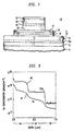
- FIG. 1 Description of FIG. 1 is first in generalized terms, and thereafter in terms of two Examples, - the first descriptive of a Pnp.
- the upper case “P” refers to a region of broad band relative to the narrow band suggested by the use of the lower case “p". Also consistent with such use, the designation, e.g. Pnp does not specify position, so that the "P" may be initially or finally grown.
- the second Example relates to the complementary structure - to the Npn.
- invention-permitted Pnp designs result in speed advantage as due to thinned base regions permitted by increased carrier concentration. Additional operating advantages result from carrier concentration increase.
- lowered parasitic resistance in turn increasing f max (the figure of merit of device frequency as affected by gain - the extrapolation of the maximum available gain v. frequency curve to 0 gain).
- Low parasitic resistance derives from lowered contact resistance and lowered sheet resistance in the base region.
- Complementary Npn structures benefit in the same manner from reduced parasitic resistance associated with reduced contact resistance there permitted in emitter and/or collector regions as tin-doped in accordance with the invention.
- FIG. 1 is used in description of the "emitter-up” as well as the inverted structure, the "collector-up” device. Description is initially in terms of the former.
- the device 10 depicted in FIG. 1 consists of substrate 11 supporting successively grown layers 12, serving as sub-collector, collector 13, and base region 14, in turn consisting of layers 15, 16 and 17. It is convenient to describe layer 16 as the functional base layer with embracing layers 15 and 17 (generally compositionally graded) serving as spacer regions (some writers refer to the entirety of region 14 as the base region).
- the emitter layer 18 is followed by optional layer 19 and finally by layers 20 and 21, the three constituting the emitter contact region in usual nomenclature.
- the collector-up device in similar terms consists of substrate 11 followed by emitter contact 12, optional emitter contact layer 12a (layer 12a, if included, is compositionally/conductively graded), emitter layer 13, base layer 14 in turn consisting of the functional base layer 16 sandwiched between spacer/graded layers 15 and 17, followed by collector layer 18, and finally by the collector contact region made up of layers 20 and 21.
- the optional graded layer 12a serving the function of graded layer 19 in the emitter-up structure, is useful as between embracing layers to assure a smooth transition (where, as in preferred embodiments, the embracing layers are of different compositions - e.g. of an AlGaAs composition (layer 18) and of the binary GaAs composition (layer 20)).
- the complementary HBT-containing IC is expected to receive early commercial attention.
- FIG. 2 is a plot of dopant level - of tin level - as produced under conditions used in the fabrication of an emitter-up structure discussed in terms of FIG. 1.
- the absc issa layer depth of 1 ⁇ m, made up in turn of high tin doped region 30 embraced between relatively low n-type conductivity regions 31 and 32 is of dimensions appropriate to present state-of-the-art integrated circuits.
- Broken curve 33 representing aluminum content, in arbitrary units, is included as showing substantial independence of attained tin doping level as between AlGaAs and GaAs regions.
- the SIMS Profile shown as solid line 34 is of particular consequence in illustrating the abruptness of n-carrier concentration change (1.5 - 2 orders of magnitude within a layer depth of 500 ⁇ ).
- Other experimental work reveals similar abruptness over a carrier concentration change of about the same size from a maximum of 1.5 x 10 19 cm -3 Sn.
- FIG. 3 contains two curves 40 and 41 in terms of tin concentration on the ordinate and layer depth on the abscissa.
- the purpose of the plot is to illustrate the abruptness of doping level attainable by means of the inventive processes.
- Experiments corresponding with both curves were designed to yield three levels of concentration of n-type carrier concentration - sublayers 42, 43 and 44 each approximately 1/3 of the total layer depth and each of a uniform carrier density.
- the objective is substantially achieved for the present processing approach (curve 40) which is representative of tin concentrations of ⁇ 5 x 10 17 ,4 x 10 18 and 2 x 10 19 for sublayers 42, 43 and 44 in that order.
- Variation in furnace temperature to yield three corresponding flux levels in the use of a prior art elemental tin source resulted in the sloping regions shown (curve 41).
- Source Temp °C
- Carrier Gas Flow Rate SCCM
- Bubbler Pressure Tir 21
- Emitter In x Ga 1-x As:Sn TMI 15 0.8 to 8.0 4.2
- Contact TEG 11.9 4.0 to 0.4 6 80 sec:300 ⁇
- Emitter Cap o GaAs:Sn TEG 11.9 4.0 6 (533 sec:2000 A) TESn -6.8 6 6 AsH 3 - 10 - 19
- Layer TMAAl 9.2 10 to 1 7 (60 sec:200 ⁇ )
Landscapes
- Engineering & Computer Science (AREA)
- Physics & Mathematics (AREA)
- Condensed Matter Physics & Semiconductors (AREA)
- General Physics & Mathematics (AREA)
- Manufacturing & Machinery (AREA)
- Computer Hardware Design (AREA)
- Microelectronics & Electronic Packaging (AREA)
- Power Engineering (AREA)
- Chemical & Material Sciences (AREA)
- Materials Engineering (AREA)
- Bipolar Transistors (AREA)
- Physical Deposition Of Substances That Are Components Of Semiconductor Devices (AREA)
Applications Claiming Priority (2)
| Application Number | Priority Date | Filing Date | Title |
|---|---|---|---|
| US662550 | 1991-02-28 | ||
| US07/662,550 US5171704A (en) | 1991-02-28 | 1991-02-28 | Gaas device fabrication utilizing metalorganic molecular beam epitaxy (mombe) |
Publications (3)
| Publication Number | Publication Date |
|---|---|
| EP0501684A2 EP0501684A2 (en) | 1992-09-02 |
| EP0501684A3 EP0501684A3 (en) | 1993-10-06 |
| EP0501684B1 true EP0501684B1 (en) | 2001-11-21 |
Family
ID=24658174
Family Applications (1)
| Application Number | Title | Priority Date | Filing Date |
|---|---|---|---|
| EP92301436A Expired - Lifetime EP0501684B1 (en) | 1991-02-28 | 1992-02-21 | Fabrication of GaAs devices with doped regions and devices so produced |
Country Status (7)
| Country | Link |
|---|---|
| US (1) | US5171704A (OSRAM) |
| EP (1) | EP0501684B1 (OSRAM) |
| JP (1) | JP3177283B2 (OSRAM) |
| KR (1) | KR100262998B1 (OSRAM) |
| CA (1) | CA2059407C (OSRAM) |
| DE (1) | DE69232213T2 (OSRAM) |
| TW (1) | TW236035B (OSRAM) |
Families Citing this family (18)
| Publication number | Priority date | Publication date | Assignee | Title |
|---|---|---|---|---|
| DE69233203T2 (de) * | 1991-11-27 | 2004-05-06 | At & T Corp. | Verfahren zum selektiven Abscheiden von Aluminium enthaltenden Schichten |
| JP3386302B2 (ja) * | 1995-12-20 | 2003-03-17 | 三菱電機株式会社 | 化合物半導体へのn型ドーピング方法およびこれを用いた化学ビーム堆積方法並びにこれらの結晶成長方法によって形成された化合物半導体結晶およびこの化合物半導体結晶によって構成された電子デバイスおよび光デバイス |
| US5960024A (en) | 1998-03-30 | 1999-09-28 | Bandwidth Unlimited, Inc. | Vertical optical cavities produced with selective area epitaxy |
| US6493372B1 (en) | 1998-04-14 | 2002-12-10 | Bandwidth 9, Inc. | Vertical cavity apparatus with tunnel junction |
| US6487231B1 (en) | 1998-04-14 | 2002-11-26 | Bandwidth 9, Inc. | Vertical cavity apparatus with tunnel junction |
| US6487230B1 (en) | 1998-04-14 | 2002-11-26 | Bandwidth 9, Inc | Vertical cavity apparatus with tunnel junction |
| US6493371B1 (en) | 1998-04-14 | 2002-12-10 | Bandwidth9, Inc. | Vertical cavity apparatus with tunnel junction |
| US5991326A (en) | 1998-04-14 | 1999-11-23 | Bandwidth9, Inc. | Lattice-relaxed verticle optical cavities |
| US6535541B1 (en) | 1998-04-14 | 2003-03-18 | Bandwidth 9, Inc | Vertical cavity apparatus with tunnel junction |
| US6493373B1 (en) | 1998-04-14 | 2002-12-10 | Bandwidth 9, Inc. | Vertical cavity apparatus with tunnel junction |
| US6760357B1 (en) | 1998-04-14 | 2004-07-06 | Bandwidth9 | Vertical cavity apparatus with tunnel junction |
| JP2000068284A (ja) * | 1998-08-19 | 2000-03-03 | Sharp Corp | ヘテロ接合バイポーラトランジスタの製造方法及びパワーアンプ |
| US6226425B1 (en) | 1999-02-24 | 2001-05-01 | Bandwidth9 | Flexible optical multiplexer |
| JP4306014B2 (ja) | 1999-05-17 | 2009-07-29 | 三菱電機株式会社 | 調速装置 |
| US6233263B1 (en) | 1999-06-04 | 2001-05-15 | Bandwidth9 | Monitoring and control assembly for wavelength stabilized optical system |
| US6275513B1 (en) | 1999-06-04 | 2001-08-14 | Bandwidth 9 | Hermetically sealed semiconductor laser device |
| CN100474512C (zh) * | 2005-01-26 | 2009-04-01 | 中国科学技术大学 | 一种ⅲ-ⅴ族半导体化合物及固熔体薄膜的制备方法 |
| US8763763B2 (en) | 2008-12-11 | 2014-07-01 | Mitsubishi Electric Corporation | Elevator apparatus having car position detection |
Family Cites Families (4)
| Publication number | Priority date | Publication date | Assignee | Title |
|---|---|---|---|---|
| US4788159A (en) * | 1986-09-18 | 1988-11-29 | Eastman Kodak Company | Process for forming a positive index waveguide |
| US4807008A (en) * | 1987-09-14 | 1989-02-21 | Rockwell International Corporation | Static memory cell using a heterostructure complementary transistor switch |
| JP2675039B2 (ja) * | 1988-02-03 | 1997-11-12 | 株式会社日立製作所 | 半導体装置 |
| JP2801624B2 (ja) * | 1988-12-09 | 1998-09-21 | 株式会社東芝 | ヘテロ接合バイポーラトランジスタ |
-
1991
- 1991-02-28 US US07/662,550 patent/US5171704A/en not_active Expired - Lifetime
-
1992
- 1992-01-15 CA CA002059407A patent/CA2059407C/en not_active Expired - Fee Related
- 1992-01-20 TW TW081100380A patent/TW236035B/zh active
- 1992-02-21 DE DE69232213T patent/DE69232213T2/de not_active Expired - Lifetime
- 1992-02-21 EP EP92301436A patent/EP0501684B1/en not_active Expired - Lifetime
- 1992-02-21 KR KR1019920002625A patent/KR100262998B1/ko not_active Expired - Lifetime
- 1992-02-28 JP JP04185192A patent/JP3177283B2/ja not_active Expired - Lifetime
Non-Patent Citations (2)
| Title |
|---|
| CHEMTRONICS, vol3, March 1988, pages 3-16 * |
| JOURNAL OF CRYSTAL GROWTH, vol 105, Nos 1/4, OCT 1990, PAGES 383-392 * |
Also Published As
| Publication number | Publication date |
|---|---|
| KR100262998B1 (ko) | 2000-09-01 |
| EP0501684A2 (en) | 1992-09-02 |
| US5171704A (en) | 1992-12-15 |
| JP3177283B2 (ja) | 2001-06-18 |
| KR920017276A (ko) | 1992-09-26 |
| CA2059407A1 (en) | 1992-08-29 |
| EP0501684A3 (en) | 1993-10-06 |
| DE69232213D1 (de) | 2002-01-03 |
| TW236035B (OSRAM) | 1994-12-11 |
| JPH04318919A (ja) | 1992-11-10 |
| CA2059407C (en) | 1999-01-12 |
| DE69232213T2 (de) | 2002-06-27 |
Similar Documents
| Publication | Publication Date | Title |
|---|---|---|
| EP0501684B1 (en) | Fabrication of GaAs devices with doped regions and devices so produced | |
| US8872231B2 (en) | Semiconductor wafer, method of producing semiconductor wafer, and electronic device | |
| EP0740350B1 (en) | Compound semiconductor device having reduced resistance | |
| US5952672A (en) | Semiconductor device and method for fabricating the same | |
| US5231298A (en) | GaAs device having a strain-free c-doped layer | |
| US5332451A (en) | Epitaxially grown compound-semiconductor crystal | |
| Razeghi et al. | High performance GaAs/GaInP heterostructure bipolar transistors grown by low-pressure metal-organic chemical vapour deposition | |
| US4902643A (en) | Method of selective epitaxial growth for compound semiconductors | |
| US5479028A (en) | III-V system compound semiconductor device and method for manufacturing the semiconductor device | |
| US7291873B2 (en) | High electron mobility epitaxial substrate | |
| US6455390B2 (en) | Method of manufacturing hetero-junction bipolar transistor | |
| EP0715357A1 (en) | Carbon-doped GaAsSb semiconductor | |
| US5858818A (en) | Formation of InGaSa p-n Junction by control of growth temperature | |
| US6797996B1 (en) | Compound semiconductor device and method for fabricating the same | |
| US4939102A (en) | Method of growing III-V semiconductor layers with high effective hole concentration | |
| KR101083612B1 (ko) | 화합물 반도체 에피택셜 기판 및 그 제조 방법 | |
| JP2001203215A (ja) | 半導体装置及びその製造方法 | |
| HK1006376A (en) | Fabrication of gaas devices with doped regions and devices so produced | |
| JP3156909B2 (ja) | 半導体積層構造の気相成長方法 | |
| CN117012814B (zh) | InP基异质结双极性晶体管的外延结构及其制备方法 | |
| US20020125498A1 (en) | Method of preparing indium phosphide heterojunction bipolar transistors | |
| JPH06267867A (ja) | 化合物半導体の結晶成長法およびこれを用いたオーミックコンタクトの形成法 | |
| JP3592922B2 (ja) | 化合物半導体基板 | |
| Izumi et al. | Chemical beam epitaxial growth of Si‐doped GaAs and InP by using silicon tetraiodide | |
| Han et al. | Growth of ultrahigh carbon-doped InGaAs and its application to InP/InGaAs (C) HBTs |
Legal Events
| Date | Code | Title | Description |
|---|---|---|---|
| PUAI | Public reference made under article 153(3) epc to a published international application that has entered the european phase |
Free format text: ORIGINAL CODE: 0009012 |
|
| AK | Designated contracting states |
Kind code of ref document: A2 Designated state(s): BE DE FR GB NL |
|
| PUAL | Search report despatched |
Free format text: ORIGINAL CODE: 0009013 |
|
| AK | Designated contracting states |
Kind code of ref document: A3 Designated state(s): BE DE FR GB NL |
|
| 17P | Request for examination filed |
Effective date: 19940324 |
|
| RAP3 | Party data changed (applicant data changed or rights of an application transferred) |
Owner name: AT&T CORP. |
|
| 17Q | First examination report despatched |
Effective date: 19961017 |
|
| RIC1 | Information provided on ipc code assigned before grant |
Free format text: 7H 01L 21/205 A, 7H 01L 21/331 B, 7H 01L 29/207 B, 7H 01L 29/737 B, 7C 30B 25/02 B |
|
| RIC1 | Information provided on ipc code assigned before grant |
Free format text: 7H 01L 21/205 A, 7H 01L 21/331 B, 7H 01L 29/207 B, 7H 01L 29/737 B, 7C 30B 25/02 B |
|
| GRAG | Despatch of communication of intention to grant |
Free format text: ORIGINAL CODE: EPIDOS AGRA |
|
| GRAG | Despatch of communication of intention to grant |
Free format text: ORIGINAL CODE: EPIDOS AGRA |
|
| GRAH | Despatch of communication of intention to grant a patent |
Free format text: ORIGINAL CODE: EPIDOS IGRA |
|
| GRAH | Despatch of communication of intention to grant a patent |
Free format text: ORIGINAL CODE: EPIDOS IGRA |
|
| GRAA | (expected) grant |
Free format text: ORIGINAL CODE: 0009210 |
|
| AK | Designated contracting states |
Kind code of ref document: B1 Designated state(s): BE DE FR GB NL |
|
| PG25 | Lapsed in a contracting state [announced via postgrant information from national office to epo] |
Ref country code: NL Free format text: LAPSE BECAUSE OF FAILURE TO SUBMIT A TRANSLATION OF THE DESCRIPTION OR TO PAY THE FEE WITHIN THE PRESCRIBED TIME-LIMIT Effective date: 20011121 Ref country code: BE Free format text: LAPSE BECAUSE OF FAILURE TO SUBMIT A TRANSLATION OF THE DESCRIPTION OR TO PAY THE FEE WITHIN THE PRESCRIBED TIME-LIMIT Effective date: 20011121 |
|
| REG | Reference to a national code |
Ref country code: GB Ref legal event code: IF02 |
|
| REF | Corresponds to: |
Ref document number: 69232213 Country of ref document: DE Date of ref document: 20020103 |
|
| NLV1 | Nl: lapsed or annulled due to failure to fulfill the requirements of art. 29p and 29m of the patents act | ||
| ET | Fr: translation filed | ||
| PLBE | No opposition filed within time limit |
Free format text: ORIGINAL CODE: 0009261 |
|
| 26N | No opposition filed | ||
| REG | Reference to a national code |
Ref country code: HK Ref legal event code: WD Ref document number: 1006376 Country of ref document: HK |
|
| PGFP | Annual fee paid to national office [announced via postgrant information from national office to epo] |
Ref country code: FR Payment date: 20110302 Year of fee payment: 20 Ref country code: DE Payment date: 20110218 Year of fee payment: 20 |
|
| PGFP | Annual fee paid to national office [announced via postgrant information from national office to epo] |
Ref country code: GB Payment date: 20110217 Year of fee payment: 20 |
|
| REG | Reference to a national code |
Ref country code: DE Ref legal event code: R071 Ref document number: 69232213 Country of ref document: DE |
|
| REG | Reference to a national code |
Ref country code: DE Ref legal event code: R071 Ref document number: 69232213 Country of ref document: DE |
|
| REG | Reference to a national code |
Ref country code: GB Ref legal event code: PE20 Expiry date: 20120220 |
|
| PG25 | Lapsed in a contracting state [announced via postgrant information from national office to epo] |
Ref country code: DE Free format text: LAPSE BECAUSE OF EXPIRATION OF PROTECTION Effective date: 20120222 |
|
| PG25 | Lapsed in a contracting state [announced via postgrant information from national office to epo] |
Ref country code: GB Free format text: LAPSE BECAUSE OF EXPIRATION OF PROTECTION Effective date: 20120220 |