EP0498662A2 - Une méthode pour la lecture de signaux issus d'un dispositif de prise d'image à l'état solide - Google Patents
Une méthode pour la lecture de signaux issus d'un dispositif de prise d'image à l'état solide Download PDFInfo
- Publication number
- EP0498662A2 EP0498662A2 EP92301041A EP92301041A EP0498662A2 EP 0498662 A2 EP0498662 A2 EP 0498662A2 EP 92301041 A EP92301041 A EP 92301041A EP 92301041 A EP92301041 A EP 92301041A EP 0498662 A2 EP0498662 A2 EP 0498662A2
- Authority
- EP
- European Patent Office
- Prior art keywords
- signal charges
- signal
- pixels
- output
- timing
- Prior art date
- Legal status (The legal status is an assumption and is not a legal conclusion. Google has not performed a legal analysis and makes no representation as to the accuracy of the status listed.)
- Granted
Links
- 238000000034 method Methods 0.000 title claims abstract description 28
- 238000003384 imaging method Methods 0.000 title claims abstract description 23
- 230000001360 synchronised effect Effects 0.000 claims abstract description 14
- 238000006243 chemical reaction Methods 0.000 claims description 9
- 230000035945 sensitivity Effects 0.000 abstract description 10
- 238000005070 sampling Methods 0.000 description 36
- 230000015556 catabolic process Effects 0.000 description 5
- 238000006731 degradation reaction Methods 0.000 description 5
- 238000009792 diffusion process Methods 0.000 description 4
- 238000010586 diagram Methods 0.000 description 3
- 230000007423 decrease Effects 0.000 description 2
- 235000008733 Citrus aurantifolia Nutrition 0.000 description 1
- 240000006909 Tilia x europaea Species 0.000 description 1
- 235000011941 Tilia x europaea Nutrition 0.000 description 1
- 238000003491 array Methods 0.000 description 1
- 238000001444 catalytic combustion detection Methods 0.000 description 1
- 238000010276 construction Methods 0.000 description 1
- 230000007812 deficiency Effects 0.000 description 1
- 230000003111 delayed effect Effects 0.000 description 1
- 230000000977 initiatory effect Effects 0.000 description 1
- 239000004571 lime Substances 0.000 description 1
- 238000012986 modification Methods 0.000 description 1
- 230000004048 modification Effects 0.000 description 1
- 239000007787 solid Substances 0.000 description 1
Images


Classifications
-
- H—ELECTRICITY
- H04—ELECTRIC COMMUNICATION TECHNIQUE
- H04N—PICTORIAL COMMUNICATION, e.g. TELEVISION
- H04N25/00—Circuitry of solid-state image sensors [SSIS]; Control thereof
- H04N25/40—Extracting pixel data from image sensors by controlling scanning circuits, e.g. by modifying the number of pixels sampled or to be sampled
- H04N25/44—Extracting pixel data from image sensors by controlling scanning circuits, e.g. by modifying the number of pixels sampled or to be sampled by partially reading an SSIS array
- H04N25/441—Extracting pixel data from image sensors by controlling scanning circuits, e.g. by modifying the number of pixels sampled or to be sampled by partially reading an SSIS array by reading contiguous pixels from selected rows or columns of the array, e.g. interlaced scanning
-
- H—ELECTRICITY
- H04—ELECTRIC COMMUNICATION TECHNIQUE
- H04N—PICTORIAL COMMUNICATION, e.g. TELEVISION
- H04N25/00—Circuitry of solid-state image sensors [SSIS]; Control thereof
- H04N25/70—SSIS architectures; Circuits associated therewith
- H04N25/71—Charge-coupled device [CCD] sensors; Charge-transfer registers specially adapted for CCD sensors
- H04N25/73—Charge-coupled device [CCD] sensors; Charge-transfer registers specially adapted for CCD sensors using interline transfer [IT]
Definitions
- the present invention relates to a method of reading out signals for a solid-state imaging device used in a video camera, image pick-up device, or the like.
- two-dimensional solid-stato imaging devices using charge transfer means are widely used in broadcast and home video cameras and the like.
- 2:1 interlaced scanning must be performed in the two-dimensional imaging devices to conform to the 2:1 interlaced scanning system of television in which two fields are traced during each frame period.
- the following describes a method of reading out signals for a solid-state imaging device in which 2:1 interlacing in such a two-dimensional solid-state imaging device is achieved by a field-integration method.
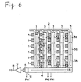
- FIG. 6 shows a schematic diagram of an interline transfer charge-coupled (CCD) area/image sensor as an example of a two-dimensional solid-state imaging device in which 2:1 interlacing is achieved by a field-integration method.
- a plurality of photoelectric convertors 1, 1, ... each comprising a photodiode, an MOS transistor, etc. are arranged in a lattice-like array (i.e., an array of rows and columns) corresponding to the pixels of the television display system.
- a gate pulse is applied to a transfer gate 2 during the vertical blanking period, charges generated by the photoelectric convertors 1, 1, ... in proportion to the light intensity are simultaneously transferrod into corresponding storage sites 3a, 3a, ...
- vertical transfer sections 3 consisting of CCDs arranged in the vertical direction alternately with the vertical arrays of photoelectric convertors 1, 1, .... After that, photoelectric conversion is performed once again by the photoelectric convertors 1, 1, ..., so that the next set of signal charges proportional to the light intensity are accumulated.
- the signal charges transferred from the photoelectric convertors 1, 1, ... to the corresponding storage sites 3a, 3a, ... in the vertical transfer sections 3 are transferred line by line, as shown by arrow (A), into corresponding storage sites (not shown) in a horizontal transfer section 4 consisting of a CCD array.
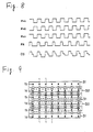
- the signal charges for one scanning line that have been transferred into the horizontal transfer section 4 are then clocked horizontally, as shown by arrow (B), toward the final stage transfer gate 6 by the clock timing'shown in Figure 8.
- the signal charges for one field are thus output line by line from the final stage transfer gate 6 to a charge detector 5, and the signal sensed by the charge detector 5 is amplified by an amplifier 7 to form a standard video signal.
- Figure 7 is a cross sectional view of the horizontal transfer section 4, transfer gate 6, and charge detector 5 of Figure 6, with applied potentials indicated.
- the above-mentioned field-integration method achieves 2:1 interlacing by reading out signals in the following manner.
- all the signal charges generated by the photoelectric convertors hereinafter referred to as pixels
- pixel pair signal charges from two vertically adjacent pixels 1a and 1b shown in Figure 6 (hereinafter simply referred to as "pixel pair") are combined and simultaneously read out into one storage site 3a in the adjacent vertical transfer section 3.
- signal charges from a pixel 1a1 and a pixel 1b1 are combined and simultaneously transferred into one storage site 3a1 in the adjacent vertical transfer section 3 (as shown by solid arrows in Figure 6); on the other hand, for an even-numbered field, signal charges from a pixel pair offset by one pixel in the vertical direction, i.e. the pixel 1b1 and a pixel 1a2, are combined and simltaneously transferred into the storage site 3a1 (as shown by dotted arrows in Figure 6).
- the space sampling points are thus arranged in a lattice-like pattern, as shown in Figure 9, at the same intervals at which the pixels 1, 1, ... are arranged.
- the timing of both a final gate transfer pulse signal ⁇ H1 ′ and a reset pulse signal ⁇ R is set so as to synchronize with a horizontal CCD drive pulse signal ⁇ H1 and a horizontal CCD drive pulse signal ⁇ H2 with the same clock cycle. Therefore, every space sampling point is positioned at the middle point between two vertically adjacent pixels constituting each pixel pair. That is, the signal charge obtained from a given space sampling point represents combined signal charges of two vertically adjacent pixels.
- the unit pixel area has been reduced to such a degree that the sensitivity characteristics of photoelectric convertors under a low light intensity are now nearing the theoretical point where shot noise associated with photoelectric conversion will become dominant. Therefore, the above method of reading out signals for a solid-state imaging device has the problem that since the signal charge of one space sampling point is obtained by combining signal charges of two vertically arranged pixels 1 and 1, the absolute signal charge amount is low per space sampling point, resulting in a drop in the signal-to-noise ratio under a low light intensity, and hence degradation in sensitivity characteristics.
- the method of reading out signals of this invention for a solid-state imaging device comprising photoelectric conversion means and charge transfer means, said photoelectric conversion means having a plurality of pixels arranged in an array of rows and columns, each of said pixels converting light to signal charges, said charge transfer means receiving said signal charges and transferring said signal charges to an output of said device overcomes the above-discussed and numerous other disadvantages and deficiencies of the prior art.
- signal charges generated in a plurality of horizontally adjacent ones of said pixels are combined in said charge transfer means and outputted at said output in a combined form.
- combinations of said plurality of horizontally adjacent ones of said pixels for combining the signal charges are periodically changed.
- video signal conforming to the 2;1 interlaced scanning is produced by changing said combinations of said plurality of horizontally adjacent ones of said pixels for combining the signal charges between an odd-numbered field and an even-numbered field.
- timing of reset clock signal for resetting said signal charges is synchronized with two clock cycles of horizontal CCD clock signals for horizontally transferring said signal charges to said output, and said signal charges of two horizontally adjacent pairs of said pixels are outputted at said output.
- timing of final gate transfer clock signal and timing of reset clock signal for resetting said signal charges are synchronized with two clock cycles of horizontal CCD clock signals for horizontally transferring said signal charges to said output, and said signal charges of two horizontally adjacent pairs of said pixels are outputted at said output.
- timing of reset clock signal for resetting said signal charges is synchronized with three or more clock cycles of horizontal CCD clock signals for horizontally transferring said signal charges to said output, and said signal charges of three or more horizontally adjacent ones of said pixels are outputted at said output.
- timing of final gate transfer clock signal and timing of reset clock signal for resetting said signal charges are synchronized with three or more clock cycles of horizontal CCD clock signals for horizontally transferring said signal charges to said output, and said signal charges of three or more horizontally adjacent ones of said pixels are outputted at said output.
- the invention described herein makes possible the objective of providing a method of reading out signals for a solid-state imaging device, which can enhance the sensitivity under a low light intensity in a simple and inexpensive way without modifying the structure of the solid-state imaging device or adding an external device.
- Figures 1A and 1B are clock timing charts of this embodiment for the horizontal transfer section 4 shown in Figure 6:
- Figure 1A is for an odd-numbered field and
- Figure 1B for an even-numbered field.
- the following detailed description deals with a method of reading out signals according to this embodiment with reference to Figures 1, 6, and 7.
- the timing of a final gate transfer clock signal ⁇ H1 ′ applied to the final transfer electrode 14 of the transfer gate 6 (see Figure 7) and the timing of a reset clock signal ⁇ R applied to a reset transistor 22 (see Figure 7) are both synchronized with two clock cycles of both horizontal CCD clock signals ⁇ H1 and ⁇ H2 , as shown in the clock timing chart of Figure 1 for the horizontal transfer section 4.
- the final gate transfer clock signal ⁇ H1 ′ goes low, causing the potential profiles in a region 18 to vary as shown by a thin dotted line in Figure 7. This causes the signal charge held at the region 18 and pertaining to the immediately preceding pixel pair to be transferred to a floating diffusion layer 21 in the charge detector 5 where the signal charge is converted to a voltage for output through the amplifier 7.
- the final gate transfer clock signal ⁇ H1 ′ goes high, making the potential at the region 18 higher than that at a region 20, as shown by a thin solid line, and thus preventing the signal charge transferred to the region 18 from being transferred to the floating diffusion layer 21.
- the horizontal CCD clock signal ⁇ H1 goes high and the horizontal CCD clock signal ⁇ H2 goes low, causing the potential profiles under electrodes 10, 11, 12, and 13 to vary as shown by a thick solid line in Figure 7, so that the signal charge transferred from one pixel pair and held at a region 16 and the signal charge transferred from another pixel pair and held at a region 15 are now transferred to the regions 18 and 17, respectively.
- the signal charge transferred from said one pixel pair is stored at the region 18.
- the horizontal CCD clock signal ⁇ H1 goes low and the horizontal CCD clock signal ⁇ H2 goes high, causing the potential profiles under the electrodes 10, 11, 12, and 13 to vary as shown by a thick dotted line in Figure 7, so that the signal charge transferred from said other pixel pair and stored at the region 17 at time (b) is now transferred to the region 16.
- the final gate transfer clock signal ⁇ H1 ′ is kept high, the signal charge of said one pixel pair, transferred to the region 18 at time (b), remains held at the region 18.
- the horizontal CCD clock signal ⁇ H1 again goes high and the horizontal CCD clock signal ⁇ H2 goes low, so that the signal charge of said other pixel pair, transferred to the region 16 at time (c), is now transferred to the region 18.
- the signal charge of said one pixel pair which has been held at the region 18 since time (b), is combined with the signal charge of said other pixel pair horizontally adjacent to said one pixel pair.
- the reset clock signal ⁇ R goes high to reset the potential of the floating diffusion layer 21 in the charge detector 5 to the reference level.
- the final gate transfer clock signal ⁇ H1 ′ goes low, so that the signal charge representing the combined signal charges of the two pixel pairs and held at the region 18 is now transferred to the floating diffusion layer 21 in the charge detector 5 where the signal charge is converted to a voltage.
- an output signal OS is output which represents the potential difference between the potential based on the combined signal charges of the four pixels 1 and the reference potential.
- the horizontal CCD clock signal ⁇ H1 goes high and the horizontal CCD clock signal ⁇ H2 goes low, initiating the transfer operation of signal charges pertaining to the next combination of two horizontally adjacent pixel pairs.
- the signal charges from the two horizontally adjacent pixel pairs comprising a total of four pixels 1 are combined to obtain a signal charge pertaining to one space sampling point.
- the space sampling points for an odd-numbered field are each taken, as shown in Figure 2, at the middle point (indicated by a circle numbered "1") between four horizontally and vertically adjacent pixels 1, 1, ... in each region 41 defined by a thin solid line.
- the space sampling points for an even-numbered field are each taken at the middle point (indicated by a square numbered "2") between four horizontally and vertically adjacent pixels 1, 1, ... in each region 42 defined by a thin dotted line.
- the signal charge amount can be increased in proportion to the increase of the photosensitive area of one space sampling point, thereby achieving an improvement in the signal-to-noise ratio. That is, a higher sensitivity can be obtained for a low light intensity although the image resolution drops to a certain degree.
- Figures 2 and 3 both show the arrangement of apace sampling points in which the space sampling points for every horizontal scan are aligned from one scanning line to the next within the same field.
- Figures 4 and 5 show the arrangement of space sampling points when the arrangement of space sampling points on the scanning lines for the same field is offset between each horizontal scan.
- the numbers in the figures indicate the scanning numbers.
- Figure 4 shows the arrangement in which the space sampling points for the same field are taken at the same points
- Figure 5 shows the arrangement in which the space sampling points for the same field are offset by one pixel in the horizontal direction between adjacent scanning limes.
- the space sampling points are arranged in a lattice-like pattern, at the same intervals at which the pixels 1 are arranged, which serves to prevent degradation in horizontal resolution that occurs with the arrangements of space sampling points shown in Figures 2 and 3.
- a signal charge pertaining to a given space sampling point for example, a space sampling point 43, 44 of scanning number "1" in an odd-numbered field
- the timing of the final gate transfer clock signal ⁇ H1 ′ and the timing of the reset clock signal ⁇ R are both synchronized with two clock cycles of the horizontal CCD clock signals ⁇ H1 and ⁇ H2 , as shown in the clock timing chart for the horizontal transfer section 4, for sampling signal charges from each pixel pair in the interline transfer CCD area/image sensor which is a two-dimensional solid-state imaging device. Therefore, the output signal OS supplied from the output terminal 8 is based on the combined signal charges obtained from two horizontally adjacent pixel pairs.
- the signal-to-noise ratio of luminance signal components can be improved (for example, shot noise is reduced by 3dB by combining signal charges from two pixel pairs), thereby providing enhanced sensitivity for applications where a low light intensity is used.
- the enhancement of sensitivity decreases the resolution to a certain degree, since the horizontal resolution decreases as the photosensitive area of one space sampling point increases.
- the resolution of the human eye also tends to drop under a low light intensity, it does not present much of a problem.
- the combination of two horizontally adjacent pixel pairs for combining the signal charges is periodically changed between each field or between adjacent scanning lines within the same field.
- the arrangement of apparent space sampling points is periodically shifted between each field or between adjacent scanning lines within the same field. This serves to prevent degradatlon in MTF characteristics.
- the timing of the final gate transfer clock signal ⁇ H1 ′ and the timing of the reset clock signal ⁇ R are both synchronized with two clock cycles of the horizontal CCD clock signals ⁇ H1 and ⁇ H2 , to store the signal charges of two horizontally adjacent pixel pairs at the region 18 as shown in Figure 7.
- the present invention is not limited to the above clocking, but only the reset clock signal ⁇ R may be synchronized with two clink cycles of the horizontal CCD clock signals ⁇ H1 and ⁇ H2 , to achieve enhancement of sensitivity in a simpler manner.
- the timing of the final gate transfer clock signal ⁇ H1 ′ and the timing of the reset pulse signal ⁇ R are both synchronized with two clock cycles of the horizontal CCD clock signals ⁇ H1 and ⁇ H2 , to combine the signal charges from two horizontally adjacent pixel pairs.
- the invention is not limited to the above clocking, but the timing of the final gate transfer clock signal ⁇ H1 ′ and the timing of the reset clock signal ⁇ R may be so set as to synchronize with three or more clock cycles of the horizontal CCD clock signals ⁇ H1 and ⁇ H2 so that signal charges from three or more horizontally adjacent pixel pairs may be combined.
- the horizontal transfer section 4 has been described as a two-electrode cell CCD array, but it will be appreciated that the invention is not restricted to this construction.
- an interline transfer CCD area/image sensor is taken as an example, but it will be appreciated that the solid-state imaging device contemplated under the present invention is not limited to the one described above.
- the method of the first embodiment is so adapted that the combination of a plurality of horizontally adjacent pixel pairs for combining the signal charges can be periodically changed, enabling the arrangement of apparent space sampling points to be shifted periodically.
- the second embodiment therefore provides the advantage, in addition to the advantages of the first embodiment, that degradation in MTF characteristics can be prevented.
Landscapes
- Engineering & Computer Science (AREA)
- Multimedia (AREA)
- Signal Processing (AREA)
- Transforming Light Signals Into Electric Signals (AREA)
- Solid State Image Pick-Up Elements (AREA)
Applications Claiming Priority (2)
| Application Number | Priority Date | Filing Date | Title |
|---|---|---|---|
| JP9117491A JPH04256364A (ja) | 1991-02-08 | 1991-02-08 | 固体撮像装置の信号読み出し方法 |
| JP17491/91 | 1991-02-08 |
Publications (3)
| Publication Number | Publication Date |
|---|---|
| EP0498662A2 true EP0498662A2 (fr) | 1992-08-12 |
| EP0498662A3 EP0498662A3 (en) | 1992-09-23 |
| EP0498662B1 EP0498662B1 (fr) | 1997-04-16 |
Family
ID=11945477
Family Applications (1)
| Application Number | Title | Priority Date | Filing Date |
|---|---|---|---|
| EP92301041A Expired - Lifetime EP0498662B1 (fr) | 1991-02-08 | 1992-02-07 | Une méthode pour la lecture de signaux issus d'un dispositif de prise d'image à l'état solide |
Country Status (5)
| Country | Link |
|---|---|
| US (1) | US5592219A (fr) |
| EP (1) | EP0498662B1 (fr) |
| JP (1) | JPH04256364A (fr) |
| KR (1) | KR960003207B1 (fr) |
| DE (1) | DE69218990T2 (fr) |
Cited By (4)
| Publication number | Priority date | Publication date | Assignee | Title |
|---|---|---|---|---|
| EP0583844A1 (fr) * | 1992-08-18 | 1994-02-23 | Koninklijke Philips Electronics N.V. | Appareil pour l'examen radiographique avec moyens de concentration de la lumière et plusieurs capteurs d'image |
| EP0588493A2 (fr) * | 1992-08-27 | 1994-03-23 | Sony Corporation | Dispositifs de couplage de charge |
| EP0763932A2 (fr) * | 1995-09-13 | 1997-03-19 | Nec Corporation | Dispositif à transfert de charges |
| EP0936806A2 (fr) | 1998-02-13 | 1999-08-18 | Sony Corporation | Procédé de commande d'un dispositif de prise d'images à l'état solide, dispositif de prise d'images à l'état solide et caméra |
Families Citing this family (6)
| Publication number | Priority date | Publication date | Assignee | Title |
|---|---|---|---|---|
| JP3397151B2 (ja) | 1998-12-10 | 2003-04-14 | 日本電気株式会社 | 固体撮像素子の駆動方法 |
| US6693670B1 (en) * | 1999-07-29 | 2004-02-17 | Vision - Sciences, Inc. | Multi-photodetector unit cell |
| US7084905B1 (en) | 2000-02-23 | 2006-08-01 | The Trustees Of Columbia University In The City Of New York | Method and apparatus for obtaining high dynamic range images |
| WO2002003675A2 (fr) * | 2000-07-05 | 2002-01-10 | Vision - Sciences Inc. | Procede de compression de gamme dynamique |
| WO2002043366A2 (fr) * | 2000-11-27 | 2002-05-30 | Vision Sciences Inc. | Capteur d'images programmable cmos a resolution |
| JP4968360B2 (ja) * | 2010-04-05 | 2012-07-04 | ソニー株式会社 | 画像表示装置 |
Citations (2)
| Publication number | Priority date | Publication date | Assignee | Title |
|---|---|---|---|---|
| EP0265302A1 (fr) * | 1986-09-19 | 1988-04-27 | Thomson-Csf | Système de prise de vues en vidéographie rapide utilisant un capteur optique matriciel à transfert de charges |
| EP0346102A2 (fr) * | 1988-06-08 | 1989-12-13 | Nippon Hoso Kyokai | Dispositif capteur d'image à l'état solide |
Family Cites Families (5)
| Publication number | Priority date | Publication date | Assignee | Title |
|---|---|---|---|---|
| US3911467A (en) * | 1974-07-25 | 1975-10-07 | Rca Corp | Interlaced readout of charge stored in charge-coupled image sensing array |
| JPS57148478A (en) * | 1981-03-09 | 1982-09-13 | Canon Inc | Solid image pickup device |
| US4805026A (en) * | 1986-02-18 | 1989-02-14 | Nec Corporation | Method for driving a CCD area image sensor in a non-interlace scanning and a structure of the CCD area image sensor for driving in the same method |
| US4995061A (en) * | 1987-12-17 | 1991-02-19 | Texas Instruments Incorporated | Two-phase CCD imager cell for TV interlace operation |
| JP2856854B2 (ja) * | 1990-07-11 | 1999-02-10 | 日本放送協会 | 固体撮像装置 |
-
1991
- 1991-02-08 JP JP9117491A patent/JPH04256364A/ja active Pending
-
1992
- 1992-02-07 DE DE69218990T patent/DE69218990T2/de not_active Expired - Fee Related
- 1992-02-07 EP EP92301041A patent/EP0498662B1/fr not_active Expired - Lifetime
- 1992-02-08 KR KR1019920001807A patent/KR960003207B1/ko not_active IP Right Cessation
-
1995
- 1995-05-11 US US08/439,445 patent/US5592219A/en not_active Expired - Fee Related
Patent Citations (2)
| Publication number | Priority date | Publication date | Assignee | Title |
|---|---|---|---|---|
| EP0265302A1 (fr) * | 1986-09-19 | 1988-04-27 | Thomson-Csf | Système de prise de vues en vidéographie rapide utilisant un capteur optique matriciel à transfert de charges |
| EP0346102A2 (fr) * | 1988-06-08 | 1989-12-13 | Nippon Hoso Kyokai | Dispositif capteur d'image à l'état solide |
Cited By (7)
| Publication number | Priority date | Publication date | Assignee | Title |
|---|---|---|---|---|
| EP0583844A1 (fr) * | 1992-08-18 | 1994-02-23 | Koninklijke Philips Electronics N.V. | Appareil pour l'examen radiographique avec moyens de concentration de la lumière et plusieurs capteurs d'image |
| EP0588493A2 (fr) * | 1992-08-27 | 1994-03-23 | Sony Corporation | Dispositifs de couplage de charge |
| EP0588493A3 (fr) * | 1992-08-27 | 1995-01-04 | Sony Corp | Dispositifs de couplage de charge. |
| EP0763932A2 (fr) * | 1995-09-13 | 1997-03-19 | Nec Corporation | Dispositif à transfert de charges |
| EP0763932A3 (fr) * | 1995-09-13 | 1999-01-20 | Nec Corporation | Dispositif à transfert de charges |
| EP0936806A2 (fr) | 1998-02-13 | 1999-08-18 | Sony Corporation | Procédé de commande d'un dispositif de prise d'images à l'état solide, dispositif de prise d'images à l'état solide et caméra |
| US7002630B1 (en) | 1998-02-13 | 2006-02-21 | Sony Corporation | Method of driving solid-state imaging device, solid-state imaging device and camera |
Also Published As
| Publication number | Publication date |
|---|---|
| DE69218990T2 (de) | 1997-10-23 |
| DE69218990D1 (de) | 1997-05-22 |
| EP0498662A3 (en) | 1992-09-23 |
| EP0498662B1 (fr) | 1997-04-16 |
| US5592219A (en) | 1997-01-07 |
| KR960003207B1 (ko) | 1996-03-06 |
| JPH04256364A (ja) | 1992-09-11 |
Similar Documents
| Publication | Publication Date | Title |
|---|---|---|
| US4831453A (en) | Solid-state imaging device having high-speed shutter function and method of realizing high-speed function in solid-state imaging device | |
| EP0346102A2 (fr) | Dispositif capteur d'image à l'état solide | |
| JP3906496B2 (ja) | 固体撮像装置およびその駆動方法、並びにカメラ | |
| US6707499B1 (en) | Technique to increase dynamic range of a CCD image sensor | |
| JP3337976B2 (ja) | 撮像装置 | |
| JPH0118629B2 (fr) | ||
| US6744466B1 (en) | Method of driving solid-state image sensor | |
| EP0866502A2 (fr) | Architecture de capteur d'images à CCD connecté à plusieurs registres de lecture | |
| US6570618B1 (en) | Solid-state image sensing apparatus, method for driving the same and camera | |
| US5592219A (en) | Method of reading out signals for a solid-state imaging device | |
| KR0135728B1 (ko) | 고체촬상장치의 구동방법 | |
| EP0876053A1 (fr) | Procédé de commande d'un capteur d'images à l'état solide | |
| US7616354B2 (en) | Image capture apparatus configured to divisionally read out accumulated charges with a plurality of fields using interlaced scanning | |
| JPS6043704B2 (ja) | 固体撮像装置 | |
| JPS59122085A (ja) | 固体撮像素子 | |
| JP2799003B2 (ja) | 固体撮像素子の駆動方式 | |
| US6760072B1 (en) | Multi-phase readout of signal charge to vertical CCD | |
| JP3010899B2 (ja) | 固体撮像装置及び固体イメージセンサの駆動制御方法 | |
| JPH01125072A (ja) | 固体撮像装置 | |
| JPS61127275A (ja) | 電荷結合形撮像素子の駆動方法 | |
| JPH03166875A (ja) | 固体撮像装置の駆動方法 | |
| JP3707910B2 (ja) | 固体撮像素子およびその駆動方法 | |
| JPH0828846B2 (ja) | 固体撮像装置 | |
| JPH09312849A (ja) | 固体撮像装置 | |
| JPS5834996B2 (ja) | カラ−コタイサツゾウソウチ |
Legal Events
| Date | Code | Title | Description |
|---|---|---|---|
| PUAI | Public reference made under article 153(3) epc to a published international application that has entered the european phase |
Free format text: ORIGINAL CODE: 0009012 |
|
| PUAL | Search report despatched |
Free format text: ORIGINAL CODE: 0009013 |
|
| AK | Designated contracting states |
Kind code of ref document: A2 Designated state(s): DE FR GB NL |
|
| AK | Designated contracting states |
Kind code of ref document: A3 Designated state(s): DE FR GB NL |
|
| 17P | Request for examination filed |
Effective date: 19921210 |
|
| 17Q | First examination report despatched |
Effective date: 19941123 |
|
| GRAG | Despatch of communication of intention to grant |
Free format text: ORIGINAL CODE: EPIDOS AGRA |
|
| GRAH | Despatch of communication of intention to grant a patent |
Free format text: ORIGINAL CODE: EPIDOS IGRA |
|
| GRAH | Despatch of communication of intention to grant a patent |
Free format text: ORIGINAL CODE: EPIDOS IGRA |
|
| GRAA | (expected) grant |
Free format text: ORIGINAL CODE: 0009210 |
|
| AK | Designated contracting states |
Kind code of ref document: B1 Designated state(s): DE FR GB NL |
|
| REF | Corresponds to: |
Ref document number: 69218990 Country of ref document: DE Date of ref document: 19970522 |
|
| ET | Fr: translation filed | ||
| PLBE | No opposition filed within time limit |
Free format text: ORIGINAL CODE: 0009261 |
|
| STAA | Information on the status of an ep patent application or granted ep patent |
Free format text: STATUS: NO OPPOSITION FILED WITHIN TIME LIMIT |
|
| 26N | No opposition filed | ||
| REG | Reference to a national code |
Ref country code: GB Ref legal event code: IF02 |
|
| PGFP | Annual fee paid to national office [announced via postgrant information from national office to epo] |
Ref country code: GB Payment date: 20060201 Year of fee payment: 15 |
|
| PGFP | Annual fee paid to national office [announced via postgrant information from national office to epo] |
Ref country code: DE Payment date: 20060202 Year of fee payment: 15 |
|
| PGFP | Annual fee paid to national office [announced via postgrant information from national office to epo] |
Ref country code: NL Payment date: 20060215 Year of fee payment: 15 |
|
| PGFP | Annual fee paid to national office [announced via postgrant information from national office to epo] |
Ref country code: FR Payment date: 20060220 Year of fee payment: 15 |
|
| GBPC | Gb: european patent ceased through non-payment of renewal fee |
Effective date: 20070207 |
|
| NLV4 | Nl: lapsed or anulled due to non-payment of the annual fee |
Effective date: 20070901 |
|
| REG | Reference to a national code |
Ref country code: FR Ref legal event code: ST Effective date: 20071030 |
|
| PG25 | Lapsed in a contracting state [announced via postgrant information from national office to epo] |
Ref country code: NL Free format text: LAPSE BECAUSE OF NON-PAYMENT OF DUE FEES Effective date: 20070901 Ref country code: DE Free format text: LAPSE BECAUSE OF NON-PAYMENT OF DUE FEES Effective date: 20070901 |
|
| PG25 | Lapsed in a contracting state [announced via postgrant information from national office to epo] |
Ref country code: GB Free format text: LAPSE BECAUSE OF NON-PAYMENT OF DUE FEES Effective date: 20070207 Ref country code: FR Free format text: LAPSE BECAUSE OF NON-PAYMENT OF DUE FEES Effective date: 20070228 |