EP0488837A2 - Méthode pour la fabrication d'un dispositif en matériau supraconducteur ayant une épaisseur réduite de film supraconducteur et le dispositif supraconducteur fabriqué de cette manière - Google Patents
Méthode pour la fabrication d'un dispositif en matériau supraconducteur ayant une épaisseur réduite de film supraconducteur et le dispositif supraconducteur fabriqué de cette manière Download PDFInfo
- Publication number
- EP0488837A2 EP0488837A2 EP91402917A EP91402917A EP0488837A2 EP 0488837 A2 EP0488837 A2 EP 0488837A2 EP 91402917 A EP91402917 A EP 91402917A EP 91402917 A EP91402917 A EP 91402917A EP 0488837 A2 EP0488837 A2 EP 0488837A2
- Authority
- EP
- European Patent Office
- Prior art keywords
- superconducting
- oxide superconductor
- gate electrode
- thin film
- oxide
- Prior art date
- Legal status (The legal status is an assumption and is not a legal conclusion. Google has not performed a legal analysis and makes no representation as to the accuracy of the status listed.)
- Granted
Links
- 238000004519 manufacturing process Methods 0.000 title claims abstract description 20
- 238000000034 method Methods 0.000 title claims description 50
- 239000002887 superconductor Substances 0.000 claims abstract description 158
- 150000001875 compounds Chemical class 0.000 claims abstract description 82
- 239000000758 substrate Substances 0.000 claims abstract description 42
- 239000012212 insulator Substances 0.000 claims abstract description 41
- 238000010438 heat treatment Methods 0.000 claims abstract description 17
- 239000000470 constituent Substances 0.000 claims abstract description 11
- 239000010409 thin film Substances 0.000 claims description 78
- 239000001301 oxygen Substances 0.000 claims description 59
- 229910052760 oxygen Inorganic materials 0.000 claims description 59
- QVGXLLKOCUKJST-UHFFFAOYSA-N atomic oxygen Chemical compound [O] QVGXLLKOCUKJST-UHFFFAOYSA-N 0.000 claims description 43
- 239000000463 material Substances 0.000 claims description 26
- 239000013078 crystal Substances 0.000 claims description 16
- -1 oxygen ions Chemical class 0.000 claims description 16
- 239000004065 semiconductor Substances 0.000 claims description 14
- XUIMIQQOPSSXEZ-UHFFFAOYSA-N Silicon Chemical compound [Si] XUIMIQQOPSSXEZ-UHFFFAOYSA-N 0.000 claims description 5
- 238000005530 etching Methods 0.000 claims description 5
- 229910021332 silicide Inorganic materials 0.000 claims description 5
- FVBUAEGBCNSCDD-UHFFFAOYSA-N silicide(4-) Chemical compound [Si-4] FVBUAEGBCNSCDD-UHFFFAOYSA-N 0.000 claims description 5
- 229910052710 silicon Inorganic materials 0.000 claims description 5
- 239000010703 silicon Substances 0.000 claims description 5
- 229910015901 Bi-Sr-Ca-Cu-O Inorganic materials 0.000 claims description 4
- QPLDLSVMHZLSFG-UHFFFAOYSA-N Copper oxide Chemical class [Cu]=O QPLDLSVMHZLSFG-UHFFFAOYSA-N 0.000 claims description 4
- 229910002480 Cu-O Inorganic materials 0.000 claims description 4
- 239000003870 refractory metal Substances 0.000 claims description 4
- 229910002370 SrTiO3 Inorganic materials 0.000 claims description 3
- 229910009203 Y-Ba-Cu-O Inorganic materials 0.000 claims description 3
- 229910002113 barium titanate Inorganic materials 0.000 claims description 3
- 239000011810 insulating material Substances 0.000 claims description 2
- 229910052737 gold Inorganic materials 0.000 claims 1
- 239000002184 metal Substances 0.000 description 6
- 229910052751 metal Inorganic materials 0.000 description 6
- 238000004544 sputter deposition Methods 0.000 description 6
- 239000004020 conductor Substances 0.000 description 4
- 238000001020 plasma etching Methods 0.000 description 4
- 238000000992 sputter etching Methods 0.000 description 4
- 238000005229 chemical vapour deposition Methods 0.000 description 3
- 239000010408 film Substances 0.000 description 3
- 230000004888 barrier function Effects 0.000 description 2
- 230000007547 defect Effects 0.000 description 2
- 230000000694 effects Effects 0.000 description 2
- 238000001451 molecular beam epitaxy Methods 0.000 description 2
- 229910052581 Si3N4 Inorganic materials 0.000 description 1
- 230000001133 acceleration Effects 0.000 description 1
- 239000011248 coating agent Substances 0.000 description 1
- 238000000576 coating method Methods 0.000 description 1
- 238000009792 diffusion process Methods 0.000 description 1
- 238000010292 electrical insulation Methods 0.000 description 1
- 238000001704 evaporation Methods 0.000 description 1
- 230000008020 evaporation Effects 0.000 description 1
- 230000005669 field effect Effects 0.000 description 1
- 238000005468 ion implantation Methods 0.000 description 1
- 150000002500 ions Chemical class 0.000 description 1
- 238000012986 modification Methods 0.000 description 1
- 230000004048 modification Effects 0.000 description 1
- 238000000926 separation method Methods 0.000 description 1
- HQVNEWCFYHHQES-UHFFFAOYSA-N silicon nitride Chemical compound N12[Si]34N5[Si]62N3[Si]51N64 HQVNEWCFYHHQES-UHFFFAOYSA-N 0.000 description 1
- 238000007738 vacuum evaporation Methods 0.000 description 1
Images


Classifications
-
- H—ELECTRICITY
- H10—SEMICONDUCTOR DEVICES; ELECTRIC SOLID-STATE DEVICES NOT OTHERWISE PROVIDED FOR
- H10N—ELECTRIC SOLID-STATE DEVICES NOT OTHERWISE PROVIDED FOR
- H10N60/00—Superconducting devices
- H10N60/20—Permanent superconducting devices
- H10N60/205—Permanent superconducting devices having three or more electrodes, e.g. transistor-like structures
- H10N60/207—Field effect devices
Definitions
- the present invention relates to a method for manufacturing a superconducting device, and more specifically to a method for manufacturing a superconducting device including an oxide superconducting layer having a partially reduced thickness portion forming a superconducting channel controlled by a gate electrode, and a superconducting device manufactured by the method.
- Typical three-terminal devices which utilize a superconductor include a so called superconducting-base transistor and a so called super-FET (field effect transistor).
- the superconducting-base transistor includes an emitter of a superconductor or a normal conductor, a tunnel barrier of an insulator, a base of a superconductor, a semiconductor isolator and a collector of a normal conductor, stacked in the named order.
- This superconducting-base transistor operates at a high speed with a low power consumption, by utilizing high speed electrons passing through the tunnel barrier.
- the super-FET includes a semiconductor layer, and a superconductor source electrode and a superconductor drain electrode which are formed closely to each other on the semiconductor layer.
- a portion of the semiconductor layer between the superconductor source electrode and the superconductor drain electrode has a greatly recessed or undercut rear surface so as to have a reduced thickness.
- a gate electrode is formed through a gate insulator layer on the recessed or undercut rear surface of the portion of the semiconductor layer between the superconductor source electrode and the superconductor drain electrode.
- a superconducting current flows through the semiconductor layer portion between the superconductor source electrode and the superconductor drain electrode due to a superconducting proximity effect, and is controlled by an applied gate voltage.
- This super-FET also operates at a high speed with a low power consumption.
- Both of the above mentioned superconducting-base transistor and the super-FET have a portion in which a semiconductor layer and a superconducting layer are stacked to each other.
- the superconductor source electrode and the superconductor drain electrode have to be located close to each other at a distance which is a few times the coherence length of the superconductor materials of the superconductor source electrode and the superconductor drain electrode.
- an oxide superconductor has a short coherence length
- a distance between the superconductor source electrode and the superconductor drain electrode has to be not greater than a few ten nanometers.
- it is very difficult to conduct a fine processing such as a fine pattern etching so as to ensure the very short separation distance. Because of this, in the prior art, it has been impossible to manufacture the super-FET composed of the oxide superconductor material.
- the conventional three-terminal superconducting device having the superconducting channel shows a modulation operation.
- the conventional three-terminal superconducting device having the superconducting channel could not realize a complete ON/OFF operation, because a carrier density is too high.
- an oxide superconductor material has a low carrier density, it is expected to form a three-terminal superconducting device which has a superconducting channel and which can realize the complete ON/OFF operation, by forming the superconducting channel of the oxide superconductor material.
- a thickness of the superconducting channel has to be made on the order of 5 nanometers.
- Another object of the present invention is to provide a method for manufacturing an FET type superconducting device including an oxide superconducting layer having an extremely thin portion forming a superconducting channel, with a good repeatability by using existing established processing techniques.
- Still another object of the present invention is to provide an FET type superconducting device having a unique structure which have overcome the above mentioned defects of the conventional ones.
- a method for manufacturing a superconducting device comprising the step of forming on a surface of the substrate a compound layer which is composed of the same constituent elements of an oxide superconductor, forming on a portion of the compound layer a gate electrode, etching portions of the compound layer at both sides of the gate electrode using the gate electrode as a mask, so that a shallow step is formed on an upper surface of the compound layer and side surfaces of the step exposed, and applying electric power to the gate electrode to heat the gate electrode so as to carry out a heat-treatment on the portion of the compound layer under the gate electrode locally, so that a gate insulator formed directly under the the gate electrode and a superconducting channel which is constituted an extremely thin superconducting region composed of the oxide superconductor and formed under the gate insulator are produced in a self alignment to the gate electrode.
- a superconducting device which comprises a superconducting device comprising a substrate, a first thin film portion of an oxide superconductor having an extremely thin thickness, a second thin film portion of an oxide superconductor positioned at one end of the first thin film portion, a third thin film portion of an oxide superconductor positioned at the other end of the first thin film portion, a first electrode formed on the second thin film portion and a second electrode formed on the third thin film portion, and a gate electrode formed on a gate insulator directly on the first thin film portion of the oxide superconductor positioned on the projecting insulating region of the substrate, so that the superconducting current flowing between the first and second electrodes through the first thin film portion of the oxide superconductor is controlled by a voltage applied to the gate electrode.
- the compound layer is an oxide superconductor thin film and the heat-treatment is carried out under high vacuum so that oxygen of the crystals of the portion of the oxide superconductor thin film just under the gate electrode escapes through the side surfaces so as to convert the portion into a non-superconducting compound oxide material and to constitute an extremely thin superconducting region under the non-superconducting compound oxide material layer.
- the oxide superconductor thin film is formed as thick as the sum of the necessary thickness of the superconducting channel and of the gate insulator.
- the compound layer does not show superconductivity but will become an oxide superconductor when the compound layer is heated in an oxygen atmosphere or when oxygen ions are injected and the heat-treatment is carried out in an oxygen atmosphere so that the oxygen is diffused through the sides surfaces into a portion of the compound layer under the gate electrode in a lateral direction so as to constitute an extremely thin superconducting region.
- oxygen ions are selectively injected into two portions of the compound layer separated from each other, so that the two separated portions of the compound layer are converted into a pair of thick superconducting regions composed of the oxide superconductor.
- the compound layer is formed of a compound oxide which is composed of the same constituent elements as those of an oxide superconductor but includes the oxygen amount less than that of the oxide superconductor, so that the compound oxide layer will be brought into an oxide superconductor when the compound oxide layer is heated in an oxygen atmosphere or when oxygen ions are injected.
- the abovementioned oxide superconductor is a high-T c (high critical temperature) oxide superconductor.
- This high-T c oxide superconductor has been studied by many researchers since the discovery of Bednorz and Müller in 1986, and is said to indicate oxide superconductor having a critical temperature of not less than 30K.
- the oxide super conductor is a high-T c copper-oxide type compound oxide superconductor including a Y-Ba-Cu O type compound oxide superconductor, a Bi-Sr-Ca-Cu-O type compound oxide superconductor and a Tl-Ba-Ca-Cu-O type compound oxide superconductor.
- the substrate, on which the oxide superconductor thin film or the compound layer is deposited can be formed of an insulating substrate, preferably an oxide single crystalline substrate such as MgO, SrTiO3, CdNdAlO4, etc. These substrate materials are very effective in forming or growing a crystalline film having a high orientation property.
- the superconducting device can be formed on a semiconductor substrate if an appropriate buffer layer is deposited thereon.
- the buffer layer on the semiconductor substrate can be formed of a double-layer coating formed of a MgAlO4 layer and a BaTiO3 layer if silicon is used as a substrate.
- the superconducting current flowing between the second and third oxide superconducting regions through the superconducting channel formed of the first oxide superconducting region is controlled by a voltage applied to the gate electrode.
- the superconducting device constitutes the super-FET.
- a thickness of the superconducting channel has to be on the order of 5 nanometers in the direction of an electric fiel created by the voltage applied to the gate electrode. This extremely thin superconducting channel can be easily realized or formed and the gate electrode, the gate insulator and the superconducting channel are arranged in a self alignment in accordance with the method of the present invention.
- a c -axis orientated oxide superconductor thin film is formed to have the thickness on the order of about 20 nanometers.
- a gate electrode is formed on the c-axis orientated oxide superconductor thin film and the c -axis orientated oxide superconductor thin film is shaped into a superconducting channel, a superconducting source region, a superconducting drain region and a gate insulator which are formed integrally.
- an upper portion of the shaped c -axis orientated oxide superconductor thin film having a thickness of more than 10 nanometers is converted into an oxide insulating layer so that a lower portion of the c -axis orientated oxide superconductor thin film becomes a superconducting channel having a thickness of about 5 nanometers.
- the portion is heated under high vacuum.
- the heat-treatment is carried out by applying electric power to the gate electrode.
- the upper portion of the oxide superconductor thin film just under the gate electrode is converted into the gate insulator by the heat-treatment which heats the portion locally, so that the gate insulator is arranged just under the gate electrode and the superconducting channel is arranged just under the gate insulator, automatically.
- Oxygen of crystals of an oxide superconductor escapes when the oxide superconductor is heated under vacuum.
- Superconducting properties of an oxide superconductor is sensitive to amounts of oxygen which is included in the crystals of the oxide superconductor. If the crystals of the oxide superconductor lack oxygen, the critical temperature of the oxide superconductor lowers considerably or the oxide superconductor loses its superconductivity.
- the upper portion of the c -axis orientated oxide superconductor thin film is converted into an oxide insulating layer substantially and the extremely thin oxide superconductor thin film can be formed.
- the thickness of the oxide insulating layer is controlled by the heat process time. It is preferable to etch the oxide superconductor film so that side surfaces of a portion which will be converted into the oxide insulating layer, which are parallel to the c-axes of crystals of oxide superconductor, are exposed, since the oxygen of crystals of oxide superconductor migrates to a direction perpendicular to the c -axis of crystals of oxide superconductor easier.
- the compound layer which does not show superconductivity but will become an oxide superconductor when which is heated in an oxygen atmosphere or when oxygen ions are injected is formed to have the thickness on the order of about 200 nanometers.
- a stacked structure including a gate insulator and a gate electrode is formed at an appropriate position on the compound layer. Oxygen ions are injected into two portions of the compound layer at both sides of the gate electrode using the gate electrode as a mask so that the portions are converted into a superconducting source region and a superconducting drain region. The portions of the compound layer at both sides of the gate electrode are etched using the gate electrode as a mask, so that a shallow step is formed on an upper surface of the compound layer.
- the portion of the compound layer under the gate electrode having a thickness of about 5 nanometers is converted into an oxide superconductor.
- the portion is heated in an oxygen atmosphere.
- the heat-treatment is carried out by applying power to the gate electrode.
- the portion of the compound layer under the gate electrode is converted into the superconducting channel by the heat-treatment which heats the portion locally, so that the superconducting channel is arranged under the gate electrode and just under the gate insulator, automatically.
- the portion of the compound layer is converted into an extremely thin oxide superconductor thin film by the heat-treatment.
- the thickness of the oxide superconductor thin film is controlled by the heat process time. It is preferable to etch the compound layer so that side surfaces of a portion which will be converted into the oxide insulating layer, which are parallel to the c-axes of crystals of compound, are exposed, since the oxygen of crystals of compound migrates to a direction perpendicular to the c -axis of crystals of compound easier.
- the extremely thin oxide superconductor thin film thus formed is very preferable in thickness and the crystal orientation to form a superconducting channel.
- the gate electrode, the gate insulator and the superconducting channel are arranged in a self alignment.
- the method in accordance with the present invention includes no process which requires high-precision for forming the superconducting channel. Therefore, the limitation in the fine processing techniques required for manufacturing the super-FET can be relaxed.
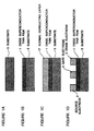
- a substrate 5 having a substantially planar principal surface is prepared.
- This substrate 5 is formed of for example, an insulator substrate such as a MgO (100) substrate, a SrTiO3 (100) substrate, a CdNdAlO4 (001) substrate or others, or a semiconductor substrate such as a silicon substrate having a principal surface coated with a buffer layer composed of an insulating film.
- the principal surface of the silicon is preferably coated with MgAlO4 by a CVD (chemical vapor deposition) and also with BaTiO3 by a sequential sputtering process.
- a c -axis orientated Y1Ba2Cu3O7 ⁇ 8 oxide superconductor thin film 1 having a thickness on the order of about 20 nanometers is deposited on the principal surface of the substrate 5, by for example an off-axis sputtering, a reactive evaporation, an MBE (molecular beam epitaxy), a CVD, etc.
- a lower portion of this oxide superconductor thin film 1 forms a superconducting channel 10 when the super-FET is completed.
- the superconducting channel is preferably formed of c -axis orientated thin film, since the c -axis orientated thin film has a large critical current density in the direction in parallel to the substrate surface.
- a condition of forming the c -axis orientated Y1Ba2Cu3O7 ⁇ 8 oxide superconductor thin film 1 by off-axis sputtering is as follows:
- the oxide superconductor thin film is preferably formed of a high-T c (high critical temperature) oxide superconductor material, particularly a high-T c copper-oxide type compound oxide superconductor material, for example, a Bi-Sr-Ca-Cu-O type compound oxide superconductor material, or a Tl-Ba-Ca-Cu-O type compound oxide superconductor material other than Y-Ba-Cu-O type compound oxide superconductor material.
- a high-T c (high critical temperature) oxide superconductor material particularly a high-T c copper-oxide type compound oxide superconductor material, for example, a Bi-Sr-Ca-Cu-O type compound oxide superconductor material, or a Tl-Ba-Ca-Cu-O type compound oxide superconductor material other than Y-Ba-Cu-O type compound oxide superconductor material.
- a normal conducting layer 17 is deposited on the oxide superconductor thin film 1.
- the normal conducting layer 17 can be deposited by a vacuum evaporation or any other suitable process.
- the normal conducting layer 17 can be formed of Au, or a refractory metal such as Ti, W or a silicide thereof.
- the normal conducting layer 17 is etched by a reactive ion etching process or an ion milling using Ar-ions so as to form a source electrode 2, a drain electrode 3 and a gate electrode 4.
- the normal conducting layer 17 is selectively etched, so as to remove all of the metal layer excluding portions which become the source electrode on the superconducting source region 12, the drain electrode on the superconducting drain region 13 and the gate electrode on the superconducting channel 10, so that the source electrode 2, the drain electrode 3 and the gate electrode 4 are formed on the oxide superconductor thin film 1 and the oxide superconductor thin film 1 is exposed excluding portions under the source electrode 2, the drain electrode 3 and the gate electrode 4.
- the exposed portions 18 of the oxide superconductor thin film 1 are selectively etched by a thickness of about 5 to 10 nanometers by a reactive ion etching process or an ion milling using Ar-ions in a self alignment to the patterned the source electrode 2, the drain electrode 3 and the gate electrode 4, so that the superconducting source region 12 and the superconducting drain region 13 are formed under the source electrode 2 and the drain electrode 3.
- a projecting portion of the oxide superconductor thin film 1 under the gate electrode 4 will be the gate insulator in future.
- the gate electrode 4 is applied electric power and heats up to more than 400 °C under a pressure of 10 ⁇ 5 Pa.
- the projecting portion of the oxide superconductor thin film 1 under the gate electrode 4 is heated locally and oxygen of the crystals of the portion escapes through side surfaces 19 so that the portion changes to the gate insulator 6.
- the portion of the oxide superconductor thin film 1 under the gate insulator 6 becomes the superconducting channel 10 which is constituted an extremely thin superconducting region, as shown in Figure 1F.
- the gate insulator 6 is formed to have a thickness sufficient to preventing a tunnel current, for example, a thickness of not less than 10 nanometers.
- An oxide superconductor loses its superconductivity when it lacks oxygen of its crystals. Therefore, after the process, the oxide which forms gate insulator 6 becomes an oxide insulator for lack of oxygen.
- the oxygen of the crystals of the oxide superconductor escapes only through sides 19, since the oxide superconductor has larger diffusion coefficients of oxygen along the a -axis and the b -axis of the crystal than along the c -axis. With this, the super-FET in accordance with the present invention is completed.
- the limitation in the fine processing technique required for manufacturing the super-FET is relaxed. Since the flatness of the upper surface of the superconducting device can be improved, it become easy to form conductor wirings in a later process. Accordingly, it is easy to manufacture the super-FET with good repeatability, and the manufactured super-FET has a stable performance.
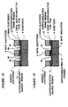
- a compound oxide layer 11 of Y1Ba2Cu3O 7-y having a thickness of for example 200 nanometers is deposited on the principal surface of the substrate 5 by for example an off-axis sputtering.
- the off-axis sputtering is performed under the same condition as that of the first embodiment. Comparing Y1Ba2Cu3O 7-y with the Y1Ba2Cu3O 7- ⁇ oxide superconductor, they are formed of the same constituent elements, but y > ⁇ , namely, Y1Ba2Cu3O 7-y contains the oxygen number less than that of Y1Ba2Cu3O 7- ⁇ so that Y1Ba2Cu3O 7-y shows an electrical insulation. But, Y1Ba2Cu3O 7-y easily becomes Y1Ba2Cu3O 7- ⁇ if Y1Ba2Cu3O 7-y is heated in an oxygen atmosphere or if oxygen ions are injected.
- a c -axis orientated thin film is preferably deposited, since the c -axis orientated thin film has a large critical current density in the direction in parallel to the substrate surface.
- an insulating layer 16 formed of for example a silicon nitride is deposited to cover the whole surface of the oxide thin film 11.
- This insulating layer 16 has a thickness sufficient to preventing a tunnel current, for example, a thickness of not less than 10 nanometers.
- the insulating layer 16 is formed of an insulating material which does not form a large density of energy levels between the superconductor thin film and the insulating layer 16.
- the insulating layer 16 is preferred to have a composition near to that of the oxide superconductor and be formed continuous on the oxide superconductor.
- a metal layer 14 for a gate electrode is deposited on the insulating layer 16.
- the metal layer 14 is preferably formed of a refractory metal such as Ti, W, etc., or Au, or a silicide thereof.
- the stacked layer of the insulating layer 16 and the metal layer 14 is selectively removed so as to form a gate electrode.
- the metal layer 14 is selectively etched by a reactive ion etching process or an ion milling using Ar-ions so as to remove all of the metal layer excluding a portion which becomes the gate electrode on the superconducting channel 10, so that the gate electrode 4 is formed.
- the insulating layer 16 is selectively etched by a reactive ion etching process or an ion milling using Ar-ions in a self alignment to the patterned gate electrode 4, so that an gate insulator 6 is left on the oxide thin film 11 and only under the patterned gate electrode 4.
- it is desired that the gate insulator 6 is side-etched in comparison with the gate electrode 4, so that the gate insulator 6 has a length shorter than that of the gate electrode 4.
- oxygen ions are ion-implanted so that a superconducting source region 12 and a superconducting drain region 13 having a substantial thickness are formed in the oxide thin film 11 as shown in Figure 2F.
- the condition for the oxygen ion-implantation is that the acceleration energy is 40KeV and the dose is 1 X 10¹⁵ to 1 X 10¹⁶ ions/cm2.
- An exposed portion of the oxide thin film 11 are etched with Ar-ions by means of an anisotropic etching, so that a shallow step is formed and side surfaces of a portion 15 of the oxide thin film 11 under the gate insulator 6 are exposed, as shown in Figure 2G.
- the gate electrode 4 is applied electric power and heats up so as to heat the portion 15 of the oxide thin film 11 in an oxygen atmosphere, so that oxygen is diffused from the exposed side surfaces of the portion 15.
- a superconducting channel 10 is formed as shown in Figure 2H.
- the oxide thin film 1 is heated simultaneously, if necessary.
- the condition for the heat-treatment is that the temperature is 350 °C, the partial oxygen pressure is 1 X 10⁴ Pa and the time is one hour.
- a portion of the oxide thin film 11 under the superconducting channel 10 is maintained in an insulating condition, and therefore, constitutes an insulating region 50.
- a source electrode 2 and a drain electrode 3 are formed on the superconducting source region 12 and the superconducting drain region 13, respectively.
- the source electrode 2 and the drain electrode 3 are formed of for example a refractory metal such as Ti, W, etc., or Au, or a silicide thereof, similarly to the gate electrode 4.
- the above mentioned super-FET is manufactured in accordance with the above mentioned process, the limitation in the fine processing technique required for manufacturing the super-FET is relaxed.
- the substantially planarized upper surface is obtained, it become easy to form conductor wirings in a later process. Accordingly, it is easy to manufacture the super-FET with good repeatability, and the manufactured super-FET has a stable performance.
- the oxide superconductor thin film can be formed of not only the Y-Ba-Cu-O type compound oxide superconductor material, but also a high-T c (high critical temperature) oxide superconductor material, particularly a high-T c copper-oxide type compound oxide superconductor material, for example a Bi-Sr-Ca-Cu-O type compound oxide superconductor material, and a Tl-Ba-Ca-Cu-O type compound oxide superconductor material.
- a high-T c oxide superconductor material particularly a high-T c copper-oxide type compound oxide superconductor material, for example a Bi-Sr-Ca-Cu-O type compound oxide superconductor material, and a Tl-Ba-Ca-Cu-O type compound oxide superconductor material.
Landscapes
- Superconductor Devices And Manufacturing Methods Thereof (AREA)
Applications Claiming Priority (4)
| Application Number | Priority Date | Filing Date | Title |
|---|---|---|---|
| JP2292816A JP2667289B2 (ja) | 1990-10-30 | 1990-10-30 | 超電導素子および作製方法 |
| JP292817/90 | 1990-10-30 | ||
| JP2292817A JP2641977B2 (ja) | 1990-10-30 | 1990-10-30 | 超電導素子の作製方法 |
| JP292816/90 | 1990-10-30 |
Publications (3)
| Publication Number | Publication Date |
|---|---|
| EP0488837A2 true EP0488837A2 (fr) | 1992-06-03 |
| EP0488837A3 EP0488837A3 (en) | 1992-08-19 |
| EP0488837B1 EP0488837B1 (fr) | 1997-04-02 |
Family
ID=26559137
Family Applications (1)
| Application Number | Title | Priority Date | Filing Date |
|---|---|---|---|
| EP91402917A Expired - Lifetime EP0488837B1 (fr) | 1990-10-30 | 1991-10-30 | Méthode pour la fabrication d'un dispositif en matériau supraconducteur ayant une épaisseur réduite de film supraconducteur et le dispositif supraconducteur fabriqué de cette manière |
Country Status (4)
| Country | Link |
|---|---|
| US (1) | US5714767A (fr) |
| EP (1) | EP0488837B1 (fr) |
| CA (1) | CA2054470C (fr) |
| DE (1) | DE69125456T2 (fr) |
Cited By (3)
| Publication number | Priority date | Publication date | Assignee | Title |
|---|---|---|---|---|
| EP0533519A2 (fr) * | 1991-08-26 | 1993-03-24 | Sumitomo Electric Industries, Ltd. | Dispositif supraconducteur ayant un canal extrêmement mince, formé en matériau supraconducteur d'oxyde et méthode pour sa fabrication |
| EP0534811A2 (fr) * | 1991-08-28 | 1993-03-31 | Sumitomo Electric Industries, Ltd. | Procédé pour la fabrication d'une couche mince supraconductrice en oxyde supraconducteur incluant des régions non-supraconductrices et procédé pour la fabraction d'un dispositif utilisant une telle couche |
| EP0551033A1 (fr) * | 1991-12-10 | 1993-07-14 | Sumitomo Electric Industries, Ltd. | Dispositif supraconducteur à canal supraconducteur extrêmement mince en oxyde supraconducteur et procédé pour sa fabrication |
Families Citing this family (3)
| Publication number | Priority date | Publication date | Assignee | Title |
|---|---|---|---|---|
| US9590161B2 (en) | 2013-11-27 | 2017-03-07 | Varian Semiconductor Equipment Associates, Inc. | Laser processing of superconductor layers |
| US9312760B2 (en) * | 2013-12-16 | 2016-04-12 | Infineon Technologies Austria Ag | Switched-mode power converter with split partitioning |
| EP4033553A1 (fr) * | 2021-01-26 | 2022-07-27 | IQM Finland Oy | Dispositif de jonction supraconducteur et sa fabrication |
Citations (4)
| Publication number | Priority date | Publication date | Assignee | Title |
|---|---|---|---|---|
| EP0280308A2 (fr) * | 1987-02-27 | 1988-08-31 | Hitachi, Ltd. | Dispositif à supraconducteur |
| EP0324044A1 (fr) * | 1988-01-15 | 1989-07-19 | International Business Machines Corporation | Dispositif à effet de champ à canal supraconducteur |
| EP0478464A1 (fr) * | 1990-09-27 | 1992-04-01 | Sumitomo Electric Industries, Ltd. | Dispositif à supraconducteur avec un canal supraconducteur extrêmement mince formé d'un matériau d'oxyde supraconducteur et procédé pour sa fabrication |
| EP0478465A1 (fr) * | 1990-09-28 | 1992-04-01 | Sumitomo Electric Industries, Ltd. | Procédé de fabrication d'un dispositif supraconducteur ayant une couche d'oxyde supraconductrice à épaisseur réduite et dispositif à supraconducteur fabriqué ainsi |
Family Cites Families (5)
| Publication number | Priority date | Publication date | Assignee | Title |
|---|---|---|---|---|
| EP0286106B1 (fr) * | 1987-04-08 | 1995-08-02 | Hitachi, Ltd. | Procédé pour fabriquer un dispositif supraconducteur |
| JPS63269585A (ja) * | 1987-04-27 | 1988-11-07 | Fujikura Ltd | ジヨセフソン接合素子 |
| JPH023938A (ja) * | 1988-06-20 | 1990-01-09 | Mitsubishi Electric Corp | 電界効果トランジスタ |
| JP2862137B2 (ja) * | 1988-08-11 | 1999-02-24 | 古河電気工業株式会社 | 超電導トランジスタ |
| JPH03191581A (ja) * | 1989-12-21 | 1991-08-21 | Fuji Electric Co Ltd | 超伝導トランジスタ |
-
1991
- 1991-10-29 CA CA002054470A patent/CA2054470C/fr not_active Expired - Fee Related
- 1991-10-30 DE DE69125456T patent/DE69125456T2/de not_active Expired - Fee Related
- 1991-10-30 EP EP91402917A patent/EP0488837B1/fr not_active Expired - Lifetime
-
1995
- 1995-11-01 US US08/551,366 patent/US5714767A/en not_active Expired - Fee Related
Patent Citations (4)
| Publication number | Priority date | Publication date | Assignee | Title |
|---|---|---|---|---|
| EP0280308A2 (fr) * | 1987-02-27 | 1988-08-31 | Hitachi, Ltd. | Dispositif à supraconducteur |
| EP0324044A1 (fr) * | 1988-01-15 | 1989-07-19 | International Business Machines Corporation | Dispositif à effet de champ à canal supraconducteur |
| EP0478464A1 (fr) * | 1990-09-27 | 1992-04-01 | Sumitomo Electric Industries, Ltd. | Dispositif à supraconducteur avec un canal supraconducteur extrêmement mince formé d'un matériau d'oxyde supraconducteur et procédé pour sa fabrication |
| EP0478465A1 (fr) * | 1990-09-28 | 1992-04-01 | Sumitomo Electric Industries, Ltd. | Procédé de fabrication d'un dispositif supraconducteur ayant une couche d'oxyde supraconductrice à épaisseur réduite et dispositif à supraconducteur fabriqué ainsi |
Non-Patent Citations (2)
| Title |
|---|
| PROCEEDINGS INTERNATIONAL ELECTRON DEVICES MEETING 11 December 1988, SAN FRANCISCO, US pages 282 - 285; Yoshida A. et al: 'Monolithic device fabrication using high-Tc superconductor' * |
| WORKSHOP ON HIGH TEMPERATURE SUPERCONDUCTING ELECTRON DEVICES 7 June 1989, SHIKABE, JAPAN pages 281 - 284; D.F.Moore et al: 'Superconducting Thin Films for Device Applications' * |
Cited By (6)
| Publication number | Priority date | Publication date | Assignee | Title |
|---|---|---|---|---|
| EP0533519A2 (fr) * | 1991-08-26 | 1993-03-24 | Sumitomo Electric Industries, Ltd. | Dispositif supraconducteur ayant un canal extrêmement mince, formé en matériau supraconducteur d'oxyde et méthode pour sa fabrication |
| EP0533519A3 (en) * | 1991-08-26 | 1993-05-05 | Sumitomo Electric Industries, Ltd. | Superconducting device having an extremely thin superconducting channel formed of oxide superconductor material and method for manufacturing the same |
| EP0534811A2 (fr) * | 1991-08-28 | 1993-03-31 | Sumitomo Electric Industries, Ltd. | Procédé pour la fabrication d'une couche mince supraconductrice en oxyde supraconducteur incluant des régions non-supraconductrices et procédé pour la fabraction d'un dispositif utilisant une telle couche |
| EP0534811A3 (fr) * | 1991-08-28 | 1993-06-02 | Sumitomo Electric Industries, Ltd. | Procédé pour la fabrication d'une couche mince supraconductrice en oxyde supraconducteur incluant des régions non-supraconductrices et procédé pour la fabraction d'un dispositif utilisant une telle couche |
| US5462919A (en) * | 1991-08-28 | 1995-10-31 | Sumitomo Electric Industries,Ltd. | Method for manufacturing superconducting thin film formed of oxide superconductor having non superconducting region and device utilizing the superconducting thin film |
| EP0551033A1 (fr) * | 1991-12-10 | 1993-07-14 | Sumitomo Electric Industries, Ltd. | Dispositif supraconducteur à canal supraconducteur extrêmement mince en oxyde supraconducteur et procédé pour sa fabrication |
Also Published As
| Publication number | Publication date |
|---|---|
| CA2054470C (fr) | 1997-07-01 |
| EP0488837B1 (fr) | 1997-04-02 |
| DE69125456T2 (de) | 1997-11-27 |
| CA2054470A1 (fr) | 1992-05-01 |
| EP0488837A3 (en) | 1992-08-19 |
| US5714767A (en) | 1998-02-03 |
| DE69125456D1 (de) | 1997-05-07 |
Similar Documents
| Publication | Publication Date | Title |
|---|---|---|
| EP0480814B1 (fr) | Dispositif supraconducteur avec un canal ultra-mince forme en matériau supraconducteur d'oxyde et procédé pour sa fabrication | |
| EP0478465B1 (fr) | Procédé de fabrication d'un dispositif supraconducteur ayant une couche d'oxyde supraconductrice à épaisseur réduite et dispositif à supraconducteur fabriqué ainsi | |
| EP0484253B1 (fr) | Dispositif supraconducteur ayant un canal extrêmement mince formé en matériau supraconducteur d'oxyde et méthode pour sa fabrication | |
| US5399546A (en) | Superconducting device having an extremely thin superconducting channel formed of oxide superconductor material | |
| CA2052380C (fr) | Dispositif a canal constitue d'une couche d'oxyde supraconducteur extremement mince et sa methode de fabrication | |
| EP0475838B1 (fr) | Dispositif supraconducteur avec un film supraconducteur de épaisseur réduite et methode pour sa fabrication | |
| EP0477103B1 (fr) | Méthode pour la fabrication d'un dispositif supraconducteur avec une couche de supraconducteur d'oxyde à une épasseur reduite et dispositif supraconducteur fabrique par cette méthode | |
| EP0488837B1 (fr) | Méthode pour la fabrication d'un dispositif en matériau supraconducteur ayant une épaisseur réduite de film supraconducteur et le dispositif supraconducteur fabriqué de cette manière | |
| EP0484251B1 (fr) | Dispositif supraconducteur ayant un canal extrêmement court formé d'un film extrêmement mince en supraconducteur d'oxyde et méthode pour sa fabrication | |
| EP0478466A1 (fr) | Dispositif à superconducteur et procédé pour sa fabrication | |
| EP0484232B1 (fr) | Dispositif supraconducteur ayant un canal supraconducteur extrêmement court en matériau supraconducteur d'oxyde et méthode pour sa fabrication | |
| EP0477063B1 (fr) | Dispositif à supraconducteur ayant une couche d'oxyde supraconductrice à épaisseur réduite et procédé pour sa fabrication | |
| EP0534811B1 (fr) | Procédé pour la fabrication d'une couche mince supraconductrice en oxyde supraconducteur incluant des régions non-supraconductrices et procédé pour la fabraction d'un dispositif utilisant une telle couche | |
| EP0478463B1 (fr) | Dispositif à supraconducteur avec un canal supraconducteur extrêmement mince formé d'un matériau d'oxyde supraconducteur | |
| JP2599500B2 (ja) | 超電導素子および作製方法 | |
| EP0545777A2 (fr) | Méthode pour la fabrication d'un couche mince en matériau supraconducteur ayant un portion à épaisseur réduite de film supraconducteur et le dispositif supraconducteur utilisant ce film supraconducteur |
Legal Events
| Date | Code | Title | Description |
|---|---|---|---|
| PUAI | Public reference made under article 153(3) epc to a published international application that has entered the european phase |
Free format text: ORIGINAL CODE: 0009012 |
|
| AK | Designated contracting states |
Kind code of ref document: A2 Designated state(s): DE FR GB |
|
| PUAL | Search report despatched |
Free format text: ORIGINAL CODE: 0009013 |
|
| AK | Designated contracting states |
Kind code of ref document: A3 Designated state(s): DE FR GB |
|
| 17P | Request for examination filed |
Effective date: 19920831 |
|
| 17Q | First examination report despatched |
Effective date: 19940826 |
|
| GRAG | Despatch of communication of intention to grant |
Free format text: ORIGINAL CODE: EPIDOS AGRA |
|
| GRAH | Despatch of communication of intention to grant a patent |
Free format text: ORIGINAL CODE: EPIDOS IGRA |
|
| GRAH | Despatch of communication of intention to grant a patent |
Free format text: ORIGINAL CODE: EPIDOS IGRA |
|
| GRAA | (expected) grant |
Free format text: ORIGINAL CODE: 0009210 |
|
| AK | Designated contracting states |
Kind code of ref document: B1 Designated state(s): DE FR GB |
|
| ET | Fr: translation filed | ||
| REF | Corresponds to: |
Ref document number: 69125456 Country of ref document: DE Date of ref document: 19970507 |
|
| PGFP | Annual fee paid to national office [announced via postgrant information from national office to epo] |
Ref country code: FR Payment date: 19971009 Year of fee payment: 7 |
|
| PGFP | Annual fee paid to national office [announced via postgrant information from national office to epo] |
Ref country code: GB Payment date: 19971021 Year of fee payment: 7 |
|
| PGFP | Annual fee paid to national office [announced via postgrant information from national office to epo] |
Ref country code: DE Payment date: 19971110 Year of fee payment: 7 |
|
| PLBE | No opposition filed within time limit |
Free format text: ORIGINAL CODE: 0009261 |
|
| STAA | Information on the status of an ep patent application or granted ep patent |
Free format text: STATUS: NO OPPOSITION FILED WITHIN TIME LIMIT |
|
| 26N | No opposition filed | ||
| PG25 | Lapsed in a contracting state [announced via postgrant information from national office to epo] |
Ref country code: GB Free format text: LAPSE BECAUSE OF NON-PAYMENT OF DUE FEES Effective date: 19981030 |
|
| GBPC | Gb: european patent ceased through non-payment of renewal fee |
Effective date: 19981030 |
|
| PG25 | Lapsed in a contracting state [announced via postgrant information from national office to epo] |
Ref country code: FR Free format text: LAPSE BECAUSE OF NON-PAYMENT OF DUE FEES Effective date: 19990630 |
|
| REG | Reference to a national code |
Ref country code: FR Ref legal event code: ST |
|
| PG25 | Lapsed in a contracting state [announced via postgrant information from national office to epo] |
Ref country code: DE Free format text: LAPSE BECAUSE OF NON-PAYMENT OF DUE FEES Effective date: 19990803 |