EP0488647A2 - Festkörper-Bildaufnahmevorrichtung - Google Patents
Festkörper-Bildaufnahmevorrichtung Download PDFInfo
- Publication number
- EP0488647A2 EP0488647A2 EP91310878A EP91310878A EP0488647A2 EP 0488647 A2 EP0488647 A2 EP 0488647A2 EP 91310878 A EP91310878 A EP 91310878A EP 91310878 A EP91310878 A EP 91310878A EP 0488647 A2 EP0488647 A2 EP 0488647A2
- Authority
- EP
- European Patent Office
- Prior art keywords
- charge
- electrode
- charge input
- light receiving
- charges
- Prior art date
- Legal status (The legal status is an assumption and is not a legal conclusion. Google has not performed a legal analysis and makes no representation as to the accuracy of the status listed.)
- Granted
Links
Images




Classifications
-
- H—ELECTRICITY
- H10—SEMICONDUCTOR DEVICES; ELECTRIC SOLID-STATE DEVICES NOT OTHERWISE PROVIDED FOR
- H10D—INORGANIC ELECTRIC SEMICONDUCTOR DEVICES
- H10D44/00—Charge transfer devices
- H10D44/40—Charge-coupled devices [CCD]
- H10D44/45—Charge-coupled devices [CCD] having field effect produced by insulated gate electrodes
- H10D44/454—Output structures
-
- H—ELECTRICITY
- H10—SEMICONDUCTOR DEVICES; ELECTRIC SOLID-STATE DEVICES NOT OTHERWISE PROVIDED FOR
- H10F—INORGANIC SEMICONDUCTOR DEVICES SENSITIVE TO INFRARED RADIATION, LIGHT, ELECTROMAGNETIC RADIATION OF SHORTER WAVELENGTH OR CORPUSCULAR RADIATION
- H10F39/00—Integrated devices, or assemblies of multiple devices, comprising at least one element covered by group H10F30/00, e.g. radiation detectors comprising photodiode arrays
- H10F39/10—Integrated devices
- H10F39/12—Image sensors
- H10F39/15—Charge-coupled device [CCD] image sensors
- H10F39/153—Two-dimensional or three-dimensional array CCD image sensors
Definitions
- the present invention relates to a solid-state imaging device and, more particularly, to a structure of a charge input means of a charge coupled device (hereinafter referred to as CCD).
- CCD charge coupled device
- a plurality of photodiodes (light receiving elements) 4 constituting a light-to-electricity conversion part are arranged in a line on a semiconductor substrate 3, and two CCDs 5 are arranged in parallel with the photodiode array.
- Respective photodiodes 4 are connected to the charge transfer part of the CCD 5 via transfer gates 6 and signal charges stored in the photodiodes 4 are transferred to the CCD 5 by the ON operation of the transfer gates 6.
- output amplifiers 7 are provided at the ends of the CCDs 5 and signal charges transferred through the CCDs 5 are amplified in the output amplifiers 7 and output from the solid-state imaging element 1.
- a charge input means 2 is provided between the initial stages of the CCDs 5, whereby charges, other than the charges from the photodiodes, are injected into the CCDs 5 from outside.
- This charge input means 2 electrically supplies charges to the CCDs 5 at the time other than the imaging mode thereby to check and calibrate the CCDs 5 and the output amplifiers 7 or to test the respective transfer electrodes constituting the CCD 5 in the production process for the CCD 5.
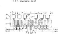
- Figure 11 is a plan view showing the structure of the charge input means 2 in detail.
- reference numeral 10 designates a charge input terminal.
- Charge input controlling gates 8 and 9, which control the quantity of charges input from the charge input terminal 10, are provided at both sides of the charge input terminal 10.
- Reference numerals 11 and 12 designate transfer electrodes of the CCD 5.
- Figure 12(a) is a diagram schematically showing a cross-section taken along a line C - C′ of figure 11 and the potential at times t1 to t4 at the charge input mode.
- Figure 12(b) schematically shows waveforms of signals that are applied to the respective terminals.
- Clock pulses I, ⁇ 1, and ⁇ 2 are applied to the charge input terminal 10, and signal input terminals of the transfer electrodes 11 and 12, respectively, and dc voltages V GIL and V GIH are applied to the signal input terminals of the charge input controlling gates 8 and 9, respectively.
- the charge input terminal 10 and the transfer electrode 12 are at "H” level while the transfer electrode 11 is at "L” level.
- the input signal I of the charge input terminal 10 becomes “L” level and charges are transferred from the charge input terminal 10 to the potential well beneath the input controlling gates 8 and 9.
- the charge input terminal 10 again becomes “H” level and the input charges Q0 are stored in the potential well beneath the input controlling gate 9.
- ⁇ 1 is at "H” level while ⁇ 2 is at “L” level and then the transfer electrode 11 becomes “H” level and the transfer electrode 12 becomes “L” level, whereby measured charges Q0 are transferred to the potential well beneath the CCD transfer electrode.
- Figure 13(a) is a diagram schematically showing a cross-section taken along a line C-C′ of figure 11 and the potential at times t1 to t3 at the imaging mode.
- Figure 13(b) schematically shows waveforms of signals applied to the respective terminals.
- Clock pulses ⁇ 1 and ⁇ 2 are applied to the signal input terminals of the transfer electrodes 11 and 12, respectively, and dc voltages V GIL and V GIH are applied to the signal input terminals of the charge input controlling gates 8 and 9, respectively.
- the transfer gate (TG) 6 is opened and the signal charges Q1 and Q2 detected respectively in the light receiving elements 4-1 and 4-2 are transferred to the potential wells beneath the corresponding transfer electrodes 11.
- the signal ⁇ 1 of the transfer electrode 11 is set to "H” level and the signal ⁇ 2 of the transfer electrode 12 is set to "L” level, whereby the signal charges Q1 and Q2 are transferred to the potential wells beneath the transfer electrodes 12 at the next stage. Thereafter, by repeating this operation, the signal charges are synchronized with the clock pulses and successively transferred.
- the array pitch of the light receiving element 4 at the charge transfer part 2 is unfavorably larger than that at the other region.
- the interval between the light receiving elements 4-1 and 4-2 is 16 microns
- the interval between the light receiving elements 4-1 is required to be 31 microns when the width of the charge input terminal is 4 microns and the widths of the charge input controlling gates 8 and 9 are 3 microns and 4 microns, respectively.
- a solid-state imaging device includes a plurality of light receiving elements, transfer gates for controlling reading-out of signal charges detected in the light receiving elements, a charge coupled device for transferring the signal charges in the light receiving elements successively by the ON operation of the transfer gates, and a charge input means provided at the initial stage of the charge coupled device.
- This charge input means is constituted by a charge input source, and a first and a second electrodes for controlling the quantity of input charges from the charge input source.
- the first electrode of the charge input means is arranged in contact with the charge input source.
- the second electrode is arranged in contact with the first electrode and connected with the light receiving element via the transfer gate or another charge coupled device.
- the second electrode serves as an electrode for controlling the quantity of input charges by applying a dc voltage thereto at the charge input mode while it serves as a first stage transfer electrode by applying a clock pulse thereto at the imaging mode.
- a solid-state imaging device includes a plurality of light receiving elements, transfer gates for controlling reading-out of signal charges detected in the light receiving elements, a charge coupled device for successively transferring signal charges in the light receiving elements by the ON operation of the transfer gates, a charge input means provided at the initial stage of the charge coupled device.
- the charge input means is constituted by a charge input source and a first, a second and a third electrodes for controlling the quantity of input charges from the charge input source.
- the first electrode is arranged in contact with the charge input source and the second electrode is arranged in contact with the first electrode.
- the third electrode is arranged in contact with the second electrode and connected to the light receiving element via the transfer gate or another charge coupled device.
- the third electrode serves as an electrode for transferring the measured charges at the charge input mode while it serves as an initial stage transfer electrode at the operation mode.
- operations at both modes can be performed without changing the array pitch of the light receiving elements at the charge input part.
- a high performance bias supply can be used for the first and second electrodes at the charge input mode.
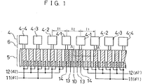
- Figure 1 is a plan view schematically showing a structure of a solid-state imaging device in accordance with a first embodiment of the present invention, in which a charge input means is provided in the center of the structure and two CCDs are serially arranged with the charge input means therebetween.
- a light-to-electricity conversion part 4 is constituted by a plurality of light receiving elements 4-1, 4-2, 4-3, 4-4 ... .
- Signal charges detected in the light-to-electricity conversion part 4 are transferred to the CCDs 5 via the transfer gates 6 by the ON operation of the transfer gates 6.
- Reference numerals 11 and 12 designate transfer electrodes of the CCDs 5 and numerals ⁇ 1 and ⁇ 2 are input signals applied to the transfer gates 11 and 12.
- Reference numeral 10 designates an electrode input terminal for electrically injecting charges into the CCDs 5 from outside.
- First charge input controlling gates 13 are provided in contact with the charge input terminal 10 and control the charges input from the charge input terminal 10.
- Common gates 14 are provided in contact with the first charge input controlling gates 13 and serve both as second charge input controlling gates and initial stage transfer electrodes. The common gates 14 serve as the second input controlling gates at the time of charge input mode and as the transfer gates like the transfer electrodes 11 at the time of imaging mode.
- the common gates 14 serve as the second charge input controlling gates with the first charge input controlling gates 13 and they function in the same way as the charge input controlling gates 8 and 9 of the prior art device.
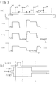
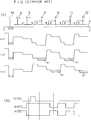
- Figure 2(a) shows a cross-section taken along a line A-A′ of figure 1 and the potential at times t1 to t4.
- Figure 2(b) schematically shows waveforms of signals applied to the respective terminals.
- Clock pulses I, ⁇ 1 and ⁇ 2 are applied to the charge input terminal 10 and the transfer electrodes 11 and 12, respectively, while dc voltages V GIL and V GIH are applied to the first charge input controlling gate 13 and the common gate 14, respectively.
- the quantity of the input charge is measured by the difference in voltages applied to the gates 13 and 14 and controlled to be a desired value.
- the transfer electrode 12 becomes "H" level and the charges Q0 are transferred to the potential well beneath the CCD transfer electrode 12.
- the charge input operation can be performed in the same way as the prior art device.
- Figure 3(a) shows a cross-section taken along a line A-A′ of figure 1 and the potential at times t1 to t3.
- Figure 3(b) schematically shows waveforms of signals applied to the respective terminals.
- a clock pulse having the same phase as that applied to the transfer electrode 11 is applied to the common gate 14 and a dc voltage is applied to the charge input controlling gate 13.
- the transfer gate TG 12 is opened and signal charges Q1 and Q2 stored in the light receiving elements 4-1 and 4-2, respectively, are transferred to the potential wells beneath the common electrode 14 and the transfer electrode 11, respectively. Thereafter, the transfer electrode 11 and the common electrode 14 are set to "L" level and the transfer electrode 12 is set to "H” level by applying clock pulses and then the signal charges Q1 beneath the common electrode 14 is transferred to the potential well beneath the transfer electrode 12 and the charges Q2 beneath the transfer electrode 11 are transferred to the potential well beneath the next stage transfer electrode. In this way, signal charges synchronized with the clock pulses are successively transferred like the prior art image sensor.
- the electrode 14 serves both as the second electrode for controlling the quantity of input charge and the initial stage transfer electrode for transferring signal charges
- the array pitch of the light receiving elements at the charge input part is as follows with employing the conventional design basis as it is.
- the width of the transfer gates 11 and 12 is 8 microns and the interval l1 between adjacent light receiving elements other than those at the charge input part is 16 microns like the prior art device
- the width of the charge input terminal 10 is 4 microns and the widths of the charge input controlling gate 13 and the common gate 14 to 3.5 microns and 5 microns, respectively
- the interval l2 between the light receiving elements 4-1 at the charge input part 2 can also be 16 microns.
- the space of the charge input part 2 can be reduced without changing the scale of the electrode input terminal and the charge input controlling gate, and the array pitch of the light receiving elements corresponding to the charge input part can be equal to the array pitch of the light receiving elements at the other parts.
- the charge input controlling electrode and the transfer electrode are constituted by the same electrode 14.
- a dc voltage is applied to the electrode 14 at the time of charge input mode so that it may serve as the second charge input controlling electrode and a clock pulse is applied thereto at the time of imaging mode so that it may serve as the transfer electrode. Therefore, the space of the charge input part 2 can be reduced and the array pitch of the light receiving elements corresponding to the charge input part can be equal to the array pitch of the light receiving elements corresponding to the other parts, whereby the pattern design can be simplified. In addition, no reduction in resolution occurs at the charge input part and a uniform resolution can be obtained in the chip.
- the present invention can be also applied to a two-dimensional solid-state imaging device.
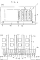
- Figure 4(a) is a plan view showing a two-dimensional solid-state imaging device in which the charge input part 2 of the above first embodiment is applied to a horizontal CCD
- figure 4(b) is a plan view showing the charge input part 2 and its vicinity in detail.
- the same references as those shown in figure 1 designate the same parts
- reference numerals 5a and 5b designate vertical CCDs and horizontal CCDs, respectively.
- the structure of the charge input part 2 is similar to that shown in figure 1 according to the first embodiment except that the common gates 14 are connected with the output terminals of the vertical CCDs 5a.
- the two-dimensional solid-state imaging device is divided in the middle and signal charges detected in the light receiving elements 4 are transferred by the vertical CCDs 5a through the transfer gates 6. Signal charges transferred from the vertical CCDs 5a are read out simultaneously by the two horizontal CCDs 5b.
- the common gates 14 are provided in the charge input part 2 between the horizontal CCDs 5b, and a dc voltage is applied to this common gates 14 at the time of charge input mode so that they may serve as charge input controlling gates and a clock pulse synchronized with the transfer electrode 11 is applied thereto at the time of imaging mode so that they may serve as transfer electrodes of the CCDs 5.
- the space of the charge input part 2 can be reduced and the array pitch of the light receiving elements corresponding to this part can be equal to the array pitch of light receiving elements corresponding to the transfer electrode parts. As a result, a reduction in resolution, which is caused by the provision of the charge input part, can be prevented.
- Figure 5 is a plan view showing another structure of two-dimensional solid-state imaging device, in which two two-dimensional solid-state imaging devices shown in figure 2 are symmetrically arranged on the semiconductor substrate 3. Also in this structure, when the charge input part 2 of the first embodiment is employed, all the light receiving elements 4 can be arranged at the same pitch, whereby the pattern production can be simplified and an uniform resolution can be obtained in the chip.
- FIG. 6 is a plan view showing a solid-state imaging device in accordance with a second embodiment of the present invention.
- a first charge input controlling gate 71 is serially connected with the charge input terminal 10.
- Second charge input controlling gates 72 are provided in contact with the first gate 71.
- the first and second gates 71 and 72 control the quantity of charges input from the charge input terminal 10.
- Common gates 73 are provided in contact with the second gates 72. This common gates 73 serve as third charge input controlling gates for transferring the charges measured in the first and second charge input controlling gates 71 and 72 at the time of charge input mode and serve as initial stage transfer electrodes for storing the signal charges from pixels for a time and thereafter transferring the same.
- Figure 7(a) is a diagram showing a cross-section taken along a line B-B′ of figure 6 and the potential at times t1 to t5.
- Figure 7(b) shows waveforms of signals applied to the respective terminals.
- Clock pulses I, 1, 2, 2F are applied to the charge input terminal 10, the transfer electrodes 11 and 12, and the common gate 73, respectively, while dc voltages V GIL and V GIH are applied to the charge input controlling gates 71 and 72.
- signals of "H” level are applied to the charge input terminal 10 and the transfer electrode 11 while signals of "L” level are applied to the transfer electrode 12 and the signal input terminal of the common gate 73.
- the level of the charge input terminal 10 is lowered and charges are transferred from the charge input terminal 10 to the potential well beneath the input controlling gates 71 and 72.
- Figure 8(a) is a diagram showing a cross-section taken along a line B-B′ of figure 6 and the potential at times t1 to t4.
- Figure 8(b) shows waveforms of signals applied to the respective terminals.
- a clock pulse having the same phase as that for the transfer electrode 12 is applied to the common gate 73 and dc voltages are applied to the charge input controlling gates 71 and 72.
- the transfer gate TG is opened and the signal charges Q1 and Q2 stored in the light receiving elements 4-1 and 4-2 are transferred to the potential wells beneath the common electrode 73 and the transfer electrode 12, respectively.
- the transfer electrode 12 and the common electrode 73 are set to "L” level and the transfer electrodes 11 are set to "H” level by applying clock pulses, whereby the signal charges Q1 beneath the common electrode 73 are transferred to the potential well beneath the transfer electrode 11 and the signal charges Q2 beneath the the transfer electrode 12 are transferred to the potential well beneath the transfer electrode 11 at the next stage.
- the transfer electrodes 12 and the common electrode 73 become "H” level and the transfer electrodes 11 become “L” level, and the signal charges Q1 and Q2 beneath the transfer electrodes 11 are transferred to the potential wells beneath the transfer electrodes 12 at the next stage.
- the array pitch of the light receiving elements at the charge input part is as follows.
- the width of the transfer electrodes 11 and 12 is 8 microns and the interval between adjacent light receiving elements other than those at the charge input part is 16 microns like the prior art device
- the width of the charge input terminal 10 is 4 microns
- the widths of the charge input controlling gates 71 and 72 to 3.5 microns and 5 microns, respectively, and the width of the common gate 73 to 5 microns
- the interval between the light receiving elements 4-1 corresponding to the charge input part is 16 micron like the first embodiment.
- the array pitch of the light receiving elements corresponding to the charge input part can be equal to that of the light receiving elements corresponding to other parts.
- the CCD is provided with the charge input means with keeping the array pitch and the resolution uniform in the chip.
- the common gate 14 in order to make the common gate 14 serve as the initial stage transfer electrode at the time of imaging mode and serve as the second charge input controlling gate at the time of charge input mode, it is necessary to apply a clock pulse to the common gate 14 at the imaging mode and a dc voltage at the charge input mode. Therefore, a clock pulse supply is always connected to the common gate 14 and when the dc voltage is applied to the common gate 14, a constant bias is generated using this clock pulse supply. Therefore, a capacitor for stabilizing the potential of the common gate 14 at the charge input time cannot be provided and a bias supply with high precision cannot be expected.
- the third charge input controlling gate is added to the structure of the charge input part 2 of the first embodiment and the common gate 73 is driven only by clock pulse at the charge input mode and the operating mode. Therefore, only dc voltage is always applied to the first and second charge input controlling gates 71 and 72, so that the charge input controlling gates 71 and 72 can be provided with a capacitor for stabilizing the potential thereof, resulting in a bias supply with high precision.
- the switching of signals at the common gate is not required and a stable bias supply can be formed in the charge input controlling gate in addition to the effects of the first embodiment.
- Figure 9(a) is a plan view showing a two-dimensional solid-state imaging device provided with the charge input part 2 of the second embodiment and figure 9(b) is a plan view showing the charge input part 2 in detail. Also in this case, the charge input means 2 can be provided at the initial stage of the horizontal CCD 5b using a normal design basis without changing the array pitch of the light receiving elements.
- a charge input means comprising a charge input source and a first and a second electrodes for controlling the quantity of the input charges is provided at the initial stage of the charge coupled device.
- the first electrode is arranged in contact with the charge input source.
- the second electrode is arranged in contact with the first electrode and connected to the light receiving element via the transfer gate or another charge coupled device.
- the second electrode serves as an electrode for controlling the quantity of the input charges at the time of charge input mode by applying a dc voltage thereto while it serves as an initial stage transfer electrode at the time of imaging mode by applying a clock pulse thereto. Therefore, the charge input means can be provided at the initial stage of the charge coupled device without changing the array pitch of the light receiving elements.
- a high performance solid-state imaging device that can test the charge coupled device electrically during its operation with keeping the resolution uniform.
- a charge input means comprising a charge input source and a first to a third electrodes for controlling the quantity of input charges is provided at the initial stage of the charge coupled device.
- the first electrode is arranged in contact with the charge input source and the second electrode is arranged in contact with the first electrode.
- the third electrode is arranged in contact with the second electrode and connected to the light receiving element via the transfer gate or another charge coupled device.
- the third electrode serves as an electrode for transferring the measured charges at the time of charge input mode while it serves as an initial stage transfer electrode at the time of imaging mode.
Landscapes
- Solid State Image Pick-Up Elements (AREA)
- Transforming Light Signals Into Electric Signals (AREA)
Priority Applications (1)
| Application Number | Priority Date | Filing Date | Title |
|---|---|---|---|
| EP98200590A EP0854517B1 (de) | 1990-11-29 | 1991-11-26 | Festkörper-Bildaufnahmevorrichtung |
Applications Claiming Priority (2)
| Application Number | Priority Date | Filing Date | Title |
|---|---|---|---|
| JP2336257A JP2604905B2 (ja) | 1990-11-29 | 1990-11-29 | 固体撮像装置 |
| JP336257/90 | 1990-11-29 |
Related Child Applications (1)
| Application Number | Title | Priority Date | Filing Date |
|---|---|---|---|
| EP98200590A Division EP0854517B1 (de) | 1990-11-29 | 1991-11-26 | Festkörper-Bildaufnahmevorrichtung |
Publications (3)
| Publication Number | Publication Date |
|---|---|
| EP0488647A2 true EP0488647A2 (de) | 1992-06-03 |
| EP0488647A3 EP0488647A3 (en) | 1992-12-23 |
| EP0488647B1 EP0488647B1 (de) | 1998-09-30 |
Family
ID=18297256
Family Applications (2)
| Application Number | Title | Priority Date | Filing Date |
|---|---|---|---|
| EP98200590A Expired - Lifetime EP0854517B1 (de) | 1990-11-29 | 1991-11-26 | Festkörper-Bildaufnahmevorrichtung |
| EP91310878A Expired - Lifetime EP0488647B1 (de) | 1990-11-29 | 1991-11-26 | Festkörper-Bildaufnahmevorrichtung |
Family Applications Before (1)
| Application Number | Title | Priority Date | Filing Date |
|---|---|---|---|
| EP98200590A Expired - Lifetime EP0854517B1 (de) | 1990-11-29 | 1991-11-26 | Festkörper-Bildaufnahmevorrichtung |
Country Status (4)
| Country | Link |
|---|---|
| US (1) | US5249055A (de) |
| EP (2) | EP0854517B1 (de) |
| JP (1) | JP2604905B2 (de) |
| DE (2) | DE69133197T2 (de) |
Cited By (1)
| Publication number | Priority date | Publication date | Assignee | Title |
|---|---|---|---|---|
| EP0552969A1 (de) * | 1992-01-22 | 1993-07-28 | Sharp Kabushiki Kaisha | Festkörperbildsensor mit transparentem Überzug und ladungsgekuppelter Anordnung |
Families Citing this family (5)
| Publication number | Priority date | Publication date | Assignee | Title |
|---|---|---|---|---|
| US6366322B1 (en) * | 1991-04-15 | 2002-04-02 | Lg Semicon Co., Ltd. | Horizontal charge coupled device of CCD image sensor |
| JPH0738077A (ja) * | 1993-07-23 | 1995-02-07 | Sony Corp | 固体撮像素子の製造方法及び固体撮像装置 |
| JP3370249B2 (ja) | 1996-12-27 | 2003-01-27 | 松下電器産業株式会社 | 固体撮像装置とその駆動方法および製造方法 |
| JP4139051B2 (ja) * | 2000-06-28 | 2008-08-27 | 富士フイルム株式会社 | リニアイメージセンサチップおよびリニアイメージセンサ |
| JP2003285249A (ja) | 2002-03-27 | 2003-10-07 | Mori Seiki Co Ltd | 工作機械の精度解析装置 |
Family Cites Families (9)
| Publication number | Priority date | Publication date | Assignee | Title |
|---|---|---|---|---|
| US3890633A (en) * | 1971-04-06 | 1975-06-17 | Rca Corp | Charge-coupled circuits |
| DE2501934C2 (de) * | 1974-01-25 | 1982-11-11 | Hughes Aircraft Co., Culver City, Calif. | Verfahren zum Betrieb eines ladungsgekoppelten Halbleiter-Bauelementes und ladungsgekoppeltes Halbleiter-Bauelement zur Durchführung dieses Verfahrens |
| JPS548428A (en) * | 1977-06-22 | 1979-01-22 | Hitachi Ltd | Address buffer circuit |
| JPS58130564A (ja) * | 1982-01-29 | 1983-08-04 | Toshiba Corp | コンパレ−タ |
| JPS60119182A (ja) * | 1983-11-30 | 1985-06-26 | Mitsubishi Electric Corp | 固体撮像素子 |
| US4647977A (en) * | 1985-01-15 | 1987-03-03 | Rca Corporation | Charge-coupled-device parallel-to-serial converter |
| US4896340A (en) * | 1985-11-01 | 1990-01-23 | Hughes Aircraft Company | Partial direct injection for signal processing system |
| JPS63226177A (ja) * | 1986-12-15 | 1988-09-20 | Mitsubishi Electric Corp | Csd型固体撮像素子 |
| US5063449A (en) * | 1988-11-18 | 1991-11-05 | Kabushiki Kaisha Toshiba | Solid-state image sensor employing a gate and diode for bias charge injection |
-
1990
- 1990-11-29 JP JP2336257A patent/JP2604905B2/ja not_active Expired - Fee Related
-
1991
- 1991-11-26 DE DE69133197T patent/DE69133197T2/de not_active Expired - Lifetime
- 1991-11-26 EP EP98200590A patent/EP0854517B1/de not_active Expired - Lifetime
- 1991-11-26 DE DE69130285T patent/DE69130285T2/de not_active Expired - Lifetime
- 1991-11-26 EP EP91310878A patent/EP0488647B1/de not_active Expired - Lifetime
- 1991-11-27 US US07/798,964 patent/US5249055A/en not_active Expired - Lifetime
Cited By (2)
| Publication number | Priority date | Publication date | Assignee | Title |
|---|---|---|---|---|
| EP0552969A1 (de) * | 1992-01-22 | 1993-07-28 | Sharp Kabushiki Kaisha | Festkörperbildsensor mit transparentem Überzug und ladungsgekuppelter Anordnung |
| US5384480A (en) * | 1992-01-22 | 1995-01-24 | Sharp Kabushiki Kaisha | Clear-mold solid-state imaging device using a charge coupled device |
Also Published As
| Publication number | Publication date |
|---|---|
| EP0488647B1 (de) | 1998-09-30 |
| JPH04207368A (ja) | 1992-07-29 |
| US5249055A (en) | 1993-09-28 |
| EP0854517A2 (de) | 1998-07-22 |
| EP0488647A3 (en) | 1992-12-23 |
| DE69133197T2 (de) | 2003-11-27 |
| EP0854517A3 (de) | 1998-08-19 |
| EP0854517B1 (de) | 2003-02-12 |
| DE69130285D1 (de) | 1998-11-05 |
| DE69133197D1 (de) | 2003-03-20 |
| JP2604905B2 (ja) | 1997-04-30 |
| DE69130285T2 (de) | 1999-06-17 |
Similar Documents
| Publication | Publication Date | Title |
|---|---|---|
| US4447735A (en) | Charge-coupled type solid-state image sensor | |
| US20010033337A1 (en) | Image pickup apparatus | |
| EP0140266B1 (de) | Schaltungsanordnung zur Kompensation von Bildelementfehlern in ladungsgekoppelten Einrichtungen | |
| EP0078038A1 (de) | Verfahren zum Betrieb eines Festkörper-Bildabtasters | |
| JPH04172085A (ja) | 固体撮像装置 | |
| US7196303B2 (en) | CCD image sensor | |
| EP0352767B1 (de) | Festkörper-Bildaufnehmer mit gemeinsamer Ausgangsleitung für Spannungen aus photoelektrischer Umwandlung | |
| US5249055A (en) | Solid-state imaging apparatus including external charge input terminal | |
| US5280511A (en) | Output circuit for a CCD with cascode depletion MOSFET loads and a feedback capacitor | |
| EP0377959B1 (de) | Verfahren zum Steuern einer Ladungsdetektorschaltung | |
| US4808834A (en) | Solid-state image sensor | |
| US5304803A (en) | Infrared imaging array | |
| US7279669B2 (en) | Method for detecting photoelectric conversion amount and photoelectric converter, method for inputting image and device for inputting image, two-dimensional image sensor and method for driving two-dimensional image sensor | |
| US4862487A (en) | Solid-state imaging device | |
| US5060072A (en) | Ccd imager with positive and mirror image output | |
| US5483283A (en) | Three level high speed clock driver for an image sensor | |
| US7638749B2 (en) | Capacitive transimpedance amplifier for CCD arrays | |
| US4752829A (en) | Multipacket charge transfer image sensor and method | |
| DE60104611T2 (de) | Halbleiterbildaufnahmevorrichtung | |
| US20030011695A1 (en) | Method and apparatus for controlling power consumption in an active pixel sensor array | |
| US4963955A (en) | Photoelectric conversion apparatus | |
| JP2003518798A (ja) | ダイオードマルチプレクサ回路及びこれを組み込んだ電子装置 | |
| EP0055530B1 (de) | Halbleiterbildsensor | |
| EP0588493B1 (de) | Ladungsgekoppelte Vorrichtungen | |
| US4833539A (en) | Circuit for reading a line-transfer photosensitive device, a line-transfer photosensitive device incorporating said circuit and a method for reading said device |
Legal Events
| Date | Code | Title | Description |
|---|---|---|---|
| PUAI | Public reference made under article 153(3) epc to a published international application that has entered the european phase |
Free format text: ORIGINAL CODE: 0009012 |
|
| AK | Designated contracting states |
Kind code of ref document: A2 Designated state(s): DE FR GB |
|
| PUAL | Search report despatched |
Free format text: ORIGINAL CODE: 0009013 |
|
| AK | Designated contracting states |
Kind code of ref document: A3 Designated state(s): DE FR GB |
|
| 17P | Request for examination filed |
Effective date: 19930125 |
|
| 17Q | First examination report despatched |
Effective date: 19950811 |
|
| GRAG | Despatch of communication of intention to grant |
Free format text: ORIGINAL CODE: EPIDOS AGRA |
|
| GRAG | Despatch of communication of intention to grant |
Free format text: ORIGINAL CODE: EPIDOS AGRA |
|
| GRAH | Despatch of communication of intention to grant a patent |
Free format text: ORIGINAL CODE: EPIDOS IGRA |
|
| GRAH | Despatch of communication of intention to grant a patent |
Free format text: ORIGINAL CODE: EPIDOS IGRA |
|
| GRAA | (expected) grant |
Free format text: ORIGINAL CODE: 0009210 |
|
| AK | Designated contracting states |
Kind code of ref document: B1 Designated state(s): DE FR GB |
|
| REF | Corresponds to: |
Ref document number: 69130285 Country of ref document: DE Date of ref document: 19981105 |
|
| ET | Fr: translation filed | ||
| PLBE | No opposition filed within time limit |
Free format text: ORIGINAL CODE: 0009261 |
|
| STAA | Information on the status of an ep patent application or granted ep patent |
Free format text: STATUS: NO OPPOSITION FILED WITHIN TIME LIMIT |
|
| 26N | No opposition filed | ||
| REG | Reference to a national code |
Ref country code: GB Ref legal event code: IF02 |
|
| PGFP | Annual fee paid to national office [announced via postgrant information from national office to epo] |
Ref country code: DE Payment date: 20091119 Year of fee payment: 19 |
|
| PGFP | Annual fee paid to national office [announced via postgrant information from national office to epo] |
Ref country code: FR Payment date: 20091123 Year of fee payment: 19 Ref country code: GB Payment date: 20091125 Year of fee payment: 19 |
|
| GBPC | Gb: european patent ceased through non-payment of renewal fee |
Effective date: 20101126 |
|
| REG | Reference to a national code |
Ref country code: FR Ref legal event code: ST Effective date: 20110801 |
|
| REG | Reference to a national code |
Ref country code: DE Ref legal event code: R119 Ref document number: 69130285 Country of ref document: DE Effective date: 20110601 Ref country code: DE Ref legal event code: R119 Ref document number: 69130285 Country of ref document: DE Effective date: 20110531 |
|
| PG25 | Lapsed in a contracting state [announced via postgrant information from national office to epo] |
Ref country code: DE Free format text: LAPSE BECAUSE OF NON-PAYMENT OF DUE FEES Effective date: 20110531 |
|
| PG25 | Lapsed in a contracting state [announced via postgrant information from national office to epo] |
Ref country code: FR Free format text: LAPSE BECAUSE OF NON-PAYMENT OF DUE FEES Effective date: 20101130 |
|
| PG25 | Lapsed in a contracting state [announced via postgrant information from national office to epo] |
Ref country code: GB Free format text: LAPSE BECAUSE OF NON-PAYMENT OF DUE FEES Effective date: 20101126 |