EP0488632A2 - A method for growing a compound semiconductor and a method for producing a semiconductor laser - Google Patents
A method for growing a compound semiconductor and a method for producing a semiconductor laser Download PDFInfo
- Publication number
- EP0488632A2 EP0488632A2 EP91310852A EP91310852A EP0488632A2 EP 0488632 A2 EP0488632 A2 EP 0488632A2 EP 91310852 A EP91310852 A EP 91310852A EP 91310852 A EP91310852 A EP 91310852A EP 0488632 A2 EP0488632 A2 EP 0488632A2
- Authority
- EP
- European Patent Office
- Prior art keywords
- substrate
- molecular beam
- layer
- gaas
- gaas layer
- Prior art date
- Legal status (The legal status is an assumption and is not a legal conclusion. Google has not performed a legal analysis and makes no representation as to the accuracy of the status listed.)
- Granted
Links
Images

Classifications
-
- H—ELECTRICITY
- H01—ELECTRIC ELEMENTS
- H01S—DEVICES USING THE PROCESS OF LIGHT AMPLIFICATION BY STIMULATED EMISSION OF RADIATION [LASER] TO AMPLIFY OR GENERATE LIGHT; DEVICES USING STIMULATED EMISSION OF ELECTROMAGNETIC RADIATION IN WAVE RANGES OTHER THAN OPTICAL
- H01S5/00—Semiconductor lasers
- H01S5/30—Structure or shape of the active region; Materials used for the active region
- H01S5/32—Structure or shape of the active region; Materials used for the active region comprising PN junctions, e.g. hetero- or double- heterostructures
- H01S5/323—Structure or shape of the active region; Materials used for the active region comprising PN junctions, e.g. hetero- or double- heterostructures in AIIIBV compounds, e.g. AlGaAs-laser, InP-based laser
- H01S5/32308—Structure or shape of the active region; Materials used for the active region comprising PN junctions, e.g. hetero- or double- heterostructures in AIIIBV compounds, e.g. AlGaAs-laser, InP-based laser emitting light at a wavelength less than 900 nm
-
- H—ELECTRICITY
- H01—ELECTRIC ELEMENTS
- H01L—SEMICONDUCTOR DEVICES NOT COVERED BY CLASS H10
- H01L21/00—Processes or apparatus adapted for the manufacture or treatment of semiconductor or solid state devices or of parts thereof
- H01L21/02—Manufacture or treatment of semiconductor devices or of parts thereof
- H01L21/02104—Forming layers
- H01L21/02365—Forming inorganic semiconducting materials on a substrate
- H01L21/02367—Substrates
- H01L21/0237—Materials
- H01L21/02387—Group 13/15 materials
- H01L21/02395—Arsenides
-
- H—ELECTRICITY
- H01—ELECTRIC ELEMENTS
- H01L—SEMICONDUCTOR DEVICES NOT COVERED BY CLASS H10
- H01L21/00—Processes or apparatus adapted for the manufacture or treatment of semiconductor or solid state devices or of parts thereof
- H01L21/02—Manufacture or treatment of semiconductor devices or of parts thereof
- H01L21/02104—Forming layers
- H01L21/02365—Forming inorganic semiconducting materials on a substrate
- H01L21/02436—Intermediate layers between substrates and deposited layers
- H01L21/02439—Materials
- H01L21/02455—Group 13/15 materials
- H01L21/02463—Arsenides
-
- H—ELECTRICITY
- H01—ELECTRIC ELEMENTS
- H01L—SEMICONDUCTOR DEVICES NOT COVERED BY CLASS H10
- H01L21/00—Processes or apparatus adapted for the manufacture or treatment of semiconductor or solid state devices or of parts thereof
- H01L21/02—Manufacture or treatment of semiconductor devices or of parts thereof
- H01L21/02104—Forming layers
- H01L21/02365—Forming inorganic semiconducting materials on a substrate
- H01L21/02518—Deposited layers
- H01L21/02521—Materials
- H01L21/02538—Group 13/15 materials
- H01L21/02546—Arsenides
-
- H—ELECTRICITY
- H01—ELECTRIC ELEMENTS
- H01L—SEMICONDUCTOR DEVICES NOT COVERED BY CLASS H10
- H01L21/00—Processes or apparatus adapted for the manufacture or treatment of semiconductor or solid state devices or of parts thereof
- H01L21/02—Manufacture or treatment of semiconductor devices or of parts thereof
- H01L21/02104—Forming layers
- H01L21/02365—Forming inorganic semiconducting materials on a substrate
- H01L21/02612—Formation types
- H01L21/02617—Deposition types
- H01L21/02631—Physical deposition at reduced pressure, e.g. MBE, sputtering, evaporation
-
- H—ELECTRICITY
- H01—ELECTRIC ELEMENTS
- H01L—SEMICONDUCTOR DEVICES NOT COVERED BY CLASS H10
- H01L21/00—Processes or apparatus adapted for the manufacture or treatment of semiconductor or solid state devices or of parts thereof
- H01L21/02—Manufacture or treatment of semiconductor devices or of parts thereof
- H01L21/02104—Forming layers
- H01L21/02365—Forming inorganic semiconducting materials on a substrate
- H01L21/02656—Special treatments
- H01L21/02658—Pretreatments
-
- H—ELECTRICITY
- H01—ELECTRIC ELEMENTS
- H01S—DEVICES USING THE PROCESS OF LIGHT AMPLIFICATION BY STIMULATED EMISSION OF RADIATION [LASER] TO AMPLIFY OR GENERATE LIGHT; DEVICES USING STIMULATED EMISSION OF ELECTROMAGNETIC RADIATION IN WAVE RANGES OTHER THAN OPTICAL
- H01S5/00—Semiconductor lasers
- H01S5/20—Structure or shape of the semiconductor body to guide the optical wave ; Confining structures perpendicular to the optical axis, e.g. index or gain guiding, stripe geometry, broad area lasers, gain tailoring, transverse or lateral reflectors, special cladding structures, MQW barrier reflection layers
- H01S5/22—Structure or shape of the semiconductor body to guide the optical wave ; Confining structures perpendicular to the optical axis, e.g. index or gain guiding, stripe geometry, broad area lasers, gain tailoring, transverse or lateral reflectors, special cladding structures, MQW barrier reflection layers having a ridge or stripe structure
- H01S5/223—Buried stripe structure
- H01S5/2231—Buried stripe structure with inner confining structure only between the active layer and the upper electrode
-
- H—ELECTRICITY
- H01—ELECTRIC ELEMENTS
- H01S—DEVICES USING THE PROCESS OF LIGHT AMPLIFICATION BY STIMULATED EMISSION OF RADIATION [LASER] TO AMPLIFY OR GENERATE LIGHT; DEVICES USING STIMULATED EMISSION OF ELECTROMAGNETIC RADIATION IN WAVE RANGES OTHER THAN OPTICAL
- H01S5/00—Semiconductor lasers
- H01S5/30—Structure or shape of the active region; Materials used for the active region
- H01S5/32—Structure or shape of the active region; Materials used for the active region comprising PN junctions, e.g. hetero- or double- heterostructures
- H01S5/323—Structure or shape of the active region; Materials used for the active region comprising PN junctions, e.g. hetero- or double- heterostructures in AIIIBV compounds, e.g. AlGaAs-laser, InP-based laser
- H01S5/32308—Structure or shape of the active region; Materials used for the active region comprising PN junctions, e.g. hetero- or double- heterostructures in AIIIBV compounds, e.g. AlGaAs-laser, InP-based laser emitting light at a wavelength less than 900 nm
- H01S5/32316—Structure or shape of the active region; Materials used for the active region comprising PN junctions, e.g. hetero- or double- heterostructures in AIIIBV compounds, e.g. AlGaAs-laser, InP-based laser emitting light at a wavelength less than 900 nm comprising only (Al)GaAs
Definitions
- the present invention relates to a method for growing GaAs and AlGaAs layers by the use of an MBE device, and more particularly to a method for producing an AlGaAs system semiconductor laser by the use of the MBE device.
- HEMTs high electron mobility transistor
- MBE device MBE device
- the surface of the GaAs substrate is oxidized by H2SO4 type etching or is heated, followed by evaporation of an oxidizing layer in the MBE device under the conditions of ultra vacuo and an atmosphere of arsenic gas.
- a GaAs buffer layer with a thickness of several ⁇ m is grown on the substrate at a relatively low temperature of 500 to 550°C.
- a satisfactory Al x Ga 1-x As layer be directly formed onto, the substrate due to the element structure (such as layer thickness and layer structure) of the semiconductor device.
- the element structure such as layer thickness and layer structure
- a GaAs buffer layer with a poor crystallinity caused by defects or impurities on the growing field on the substrate has an adverse effect on the characteristics of the device, for example when an active region (a channel region 41 ) of an HEMT shown in Figure 4 is disposed close to a buffer layer 40 and the characteristics of the buffer layer 40 have such an influence on those of the HEMT as a reduced mobility of channel electrons caused by scattering impurities, it is required that a satisfactory GaAs buffer layer is directly formed on the substrate.
- a typical method for producing a semiconductor laser by the use of the MBE device is disclosed in Japanese Patent Publication No. 1-37873.
- a semiconductor substrate is taken out of the MBE device after a first growing layer is formed in the first growing step.
- a striped groove with a predetermined width and a depth which reaches a GaAs light absorption layer of the first growing layer is formed in the photolithography and etching step.
- impurities such as oxide adhere to the etched portion, i.e., the surface of the light absorption layer. These impurities are evaporated by thermal cleaning with irradiating arsenic (As).
- a second growing layer is formed in the second growing step by the use of the MBE.
- a very clean upper surface of a clad layer can be obtained by evaporating these impurities as well as the GaAs light absorption layer in the active region. Then, a growing layer of high quality containing no impurities can be obtained in the second growing step by the use of the MBE.
- the surface condition in cleaning is greatly influenced by the cleanliness of the surface of the etched portion, intensity of irradiation of As, the temperature of the heat treatment and the difference in level of the first growing layer formed by etching. Therefore, very limiting conditions are required to be set in order to get a surface having good quality and satisfactory flatness. Particularly, the dispersion of the cleanliness of the etched surface leads to the dispersion of the evaporation rate of the surface. As a result, the etched GaAs layer partially remains and a flat thermal cleaning surface with high repeatability cannot be obtained. The microscopic unevenness caused after etching the substrate is enlarged by thermal etching thereafter.
- the evaporation rate greatly depends upon the temperature or arsenic pressure on the substrate, there arises a dispersion in the evaporation rate when a dispersion exists in the temperature or arsenic pressure, and it is difficult to obtain a flat evaporation surface. Because of these phenomena, a part of the etched portion (GaAs layer) remains between the first growing layer (the clad layer of the Al x Ga 1-x As layer) and the second growing layer (the clad layer of the Al x Ga 1-x As layer in the above-mentioned semiconductor laser structure, thereby having adverse effects on the laser oscillation characteristics (i.e., decreasing luminous efficiency). Accordingly, there arise problems of yield and/or lack of uniformity.
- the method for growing a compound semiconductor of this invention which overcomes the above-discussed and numerous other disadvantages and deficiencies of the prior art, in which Al x Ga 1-x As (0 ⁇ x ⁇ 1) is grown on a GaAs layer formed on a compound semiconductor substrate by the use of a molecular beam epitaxial device, comprises: a first step of thermal cleaning of the GaAs layer surface by raising the temperature of the substrate and irradiating an arsenic molecular beam onto the substrate prior to the growth of Al x Ga 1-x As; and a second step of etching removal of the GaAs layer by raising the temperature of the substrate further than the first step and irradiating a gallium molecular beam and an arsenic molecular beam at the same time onto the substrate, in which a growth rate of the GaAs layer is set lower than that of an evaporation rate thereof.
- a method for producing a semiconductor laser by the use of a molecular beam epitaxial device in which a layered structure is formed on a substrate by a continuous molecular beam epitaxial growth, then the layered structure is etched into a desired shape so that the substrate surface becomes a GaAs layer, and another layered structure is formed on the substrate by the continuous molecular beam epitaxial growth comprises; a first step of thermal cleaning of the GaAs layer surface by raising the temperature of the substrate and irradiating an arsenic molecular beam onto the substrate prior to the regrowth; and a second step of etching removal of the GaAs layer by rising the temperature of the substrate further than the first step and irradiating at the same time a gallium molecular beam and an arsenic molecular beam onto the substrate, in which a growth rate of the GaAs layer is set lower than that of an evaporation rate thereof.
- the substrate is maintained at a high temperature in the range of 600 to 800°C with the simultaneous irradiation of the Ga molecular beam and the As molecular beam.
- the GaAs layer is deposited and the surface of the semiconductor substrate is made flat.
- the thermal etching of the GaAs layer is effected, whereby a flat and clean etched surface can be realized.
- the present invention comprises the simultaneous irradiation of the Ga molecular beam and the As molecular beam, and the heat treatment process at high temperatures in which the GaAs layer can be evaporated.
- the invention described herein makes possible the objectives of (1) providing an epitaxial growth method enabling a construction in which an AlGaAs layer is directly deposited on a semiconductor (AlGaAs system) substrate or in which a GaAs buffer layer having poor crystalline characteristics is not included; and (2) providing a method for producing a semiconductor laser in which a partially remained portion of the etched surface caused by the dispersion of precision of thermal etching conditions and by the dispersion of photolithography and etching and unevenness caused by this portion can be eliminated and a flat thermal etching surface can be formed, thereby realizing satisfactory semiconductor laser characteristics.
- Figures 1(a) and 1(b) are schematic sectional views illustrating an embodiment of the epitaxial growth method according to the present invention.
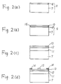
- Figures 2(a) to 2(d) are schematic sectional views illustrating an embodiment of a method for producing an electron device (HEMT or the like) according to the present invention.
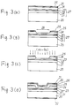
- Figures 3(a) to 3(d) are schematic sectional views illustrating an embodiment of a method for producing a semiconductor laser according to the present invention.
- Figure 4 is a schematic sectional view illustrating a method for producing a conventional electron device (HEMT).
- HEMT conventional electron device
- Figures 1(a) and 1(b) are sectional views illustrating an embodiment of an epitaxial growth method according to the present invention.
- a compound semiconductor substrate 3 (consisting of an Al x Ga 1-x As layer 2 and a GaAs substrate 1 ) on which a GaAs layer 4 with a thickness of several thousand ⁇ has been previously deposited by an epitaxial growth method such as the MBE method or the MOCVD method is placed in an MBE apparatus.
- the compound semiconductor substrate 3 is heated to a desired temperature (about 630°C) while being irradiated with an As molecular beam so that the oxidizing layer of the surface of the GaAs layer 4 is removed by evaporation (see Figure 1(a) ).
- the compound semiconductor substrate 3 is heated with a simultaneous irradiation of a predetermined amount of the Ga (gallium) molecular beam and the As molecular beam, and is maintained at a temperature in the range of 720 to 760°C for about thirty minutes while forming a first GaAs layer (a layer for evaporation).
- the amount of the incidence molecular beams of Ga is kept so as to make the growth rate of GaAs layer lower than the evaporation rate thereof.
- the GaAs layer is evaporated (i.e., thermal etching is effected), and a flat and clean interface 5 is obtained.
- an AlGaAs layer 6 is deposited by irradiating an Al (aluminum) molecular beam successively.
- Al (aluminum) molecular beam a satisfactory flat epitaxial layer of the AlGaAs layer 6 which is directly deposited on the compound semiconductor substrate 3 with no buffer layer formed therebetween (see Figure 1(b) ).
- Figures 2(a) to 2(d) are sectional views illustrating an embodiment of a method for producing an electron device (HEMT) according to the present invention.
- Figure 2(a) shows a semi-insulating GaAs substrate 9 (consisting of a first GaAs layer for evaporation 8 and a layer which is not evaporated 7 ) used for the MBE growth, the surface of which is cleaned by a predetermined etching treatment.
- the GaAs substrate 9 is placed in the MBE device, heated to a desired temperature in the range of 620 to 650°C while being irradiated with the As molecular beam, and a natural oxide film adhered to the surface of the GaAs substrate 9 is evaporated, thereby obtaining a clean GaAs surface.
- the resulting GaAs substrate 9 is heated to a temperature of 720 to 750°C with simultaneous irradiation of a predetermined amount of the Ga molecular beam and the As molecular beam, and a growing interface 16 and the first GaAs layer for evaporation 8 (the upper portion of the semi-insulating GaAs substrate 9 ) are evaporated while a second GaAs layer for evaporation 10 is formed (see Figure 2(b) ).
- the first and the second GaAs layers for evaporation 8 and 10 are removed by evaporation, thereby obtaining a very flat clean surface of the substrate.
- An undoped GaAs layer 11 , an N-type Al 0.3 Ga 0.7 As layer 12 and an N-type GaAs layer 13 are successively formed with a predetermined growth temperature (about 500°C) kept on the substrate (see Figure 2(c) ).
- the thus obtained HEMT structure substrate is taken out of the MBE device.
- An AuGe/Ni/Au N-type Ohmic electrode 14 and a Ti/Pt/Au P-type Schottky electrode are formed on the substrate by vacuum evaporation as shown in Figure 2(d) . In this way, an HEMT structure with a clear and flat growing interface on the substrate can be produced.
- Figures 3(a) to 3(d) show an embodiment of a method for producing a semiconductor laser according to the present invention.
- a light absorption layer 24 made of GaAs, an evaporation-preventing layer 25 made of an AlGaAs layer, a regrowth protection layer 26 made of GaAs and a Double Hetero (DH) structure 27 made of AlGaAs layers are epitaxially grown on an N-type (100) GaAs substrate 20 by the epitaxial growth method such as the MBE method and the MOCVD method (see Figure 3(a) ).
- the compound semiconductor substrate on which the above DH structure is grown is temporarily taken out of the growing device, a stripe-shaped groove (having a width of 3 to 5 ⁇ m) is formed in a region which is to be a current passage 28 by predetermined photolithography and etching steps, leaving the GaAs light absorption layer 24 of 1000 ⁇ thickness (see Figure 3(b) ). Then, the compound semiconductor substrate with this striped-shaped groove is again placed in the MBE device and the As molecular beam is irradiated until a predetermined temperature (620 to 650°C) is obtained.
- a predetermined temperature 620 to 650°C
- the temperature of the substrate is kept at a temperature in the range of 720 to 760°C for several ten of minutes.
- the amount of the Ga molecular beam at this time is set so that the evaporation rate of the GaAs is higher than the growth rate thereof.
- a GaAs layer is deposited and evaporated at the same time, resulting in evaporating the exposed GaAs layer and exposing a clear AlGaAs layer as shown in Figure 3(c) .
- the exposed AlGaAs layer includes a first AlGaAs clad layer 23 in the current passage 28 and the evaporation-preventing layer 25 made of AlGaAs on the other region.
- a second AlGaAs clad layer 29 and a GaAs cap layer 30 are successively formed by combined irradiation of the Al molecular beam and Be molecular beam. Then the substrate is taken out of the MBE device, and a semiconductor laser structure is produced by forming a P-type electrode 31 and an N-type electrode 32 by vacuum evaporation.
- the thermal etching is effected at a high temperature (600 to 800°C) while the Ga molecular beam and the As molecular beam are simultaneously irradiated.
- the etched surface is made flat owing to the GaAs layer formed by the above simultaneous irradiation, and the GaAs buffer layer and the layer in which impurities remain are removed by the thermal etching at a high temperature. Accordingly, in the present example, a satisfactory flat thermal etching surface, in which there is no GaAs buffer layer or unevenness of the layer having impurities and the etched surface, or unevenness caused by the dispersion of the thermal etching conditions, can be obtained.
Abstract
Description
- The present invention relates to a method for growing GaAs and AlGaAs layers by the use of an MBE device, and more particularly to a method for producing an AlGaAs system semiconductor laser by the use of the MBE device.
- In recent years, a method for producing high electron mobility transistor (HEMTs) and semiconductor lasers as an AlGaAs system semiconductor device by the use of an MBE device has been proposed. These devices function by epitaxially growing an AlGaAs layer and a GaAs layer on a GaAs substrate.
- In the epitaxial growth used for producing an AlGaAs system device by the MBE device, cleanliness and unevenness of the substrate surface has a great influence on the quality of the epitaxial layer. In order to make a GaAs surface clean, the surface of the GaAs substrate is oxidized by H₂SO₄ type etching or is heated, followed by evaporation of an oxidizing layer in the MBE device under the conditions of ultra vacuo and an atmosphere of arsenic gas. In order to provide the substrate with a flat surface, a GaAs buffer layer with a thickness of several µm is grown on the substrate at a relatively low temperature of 500 to 550°C. However, in some cases it is required that a satisfactory AlxGa1-xAs layer be directly formed onto, the substrate due to the element structure (such as layer thickness and layer structure) of the semiconductor device. Moreover, when a GaAs buffer layer with a poor crystallinity caused by defects or impurities on the growing field on the substrate has an adverse effect on the characteristics of the device, for example when an active region (a channel region 41) of an HEMT shown in Figure 4 is disposed close to a
buffer layer 40 and the characteristics of thebuffer layer 40 have such an influence on those of the HEMT as a reduced mobility of channel electrons caused by scattering impurities, it is required that a satisfactory GaAs buffer layer is directly formed on the substrate. - A typical method for producing a semiconductor laser by the use of the MBE device is disclosed in Japanese Patent Publication No. 1-37873. In this method, a semiconductor substrate is taken out of the MBE device after a first growing layer is formed in the first growing step. Then, a striped groove with a predetermined width and a depth which reaches a GaAs light absorption layer of the first growing layer is formed in the photolithography and etching step. In this step, impurities such as oxide adhere to the etched portion, i.e., the surface of the light absorption layer. These impurities are evaporated by thermal cleaning with irradiating arsenic (As). Then, a second growing layer is formed in the second growing step by the use of the MBE.
- According to the above method for producing semiconductor lasers, a very clean upper surface of a clad layer can be obtained by evaporating these impurities as well as the GaAs light absorption layer in the active region. Then, a growing layer of high quality containing no impurities can be obtained in the second growing step by the use of the MBE.
- However, in the above cleaning step by the thermal etching using only As, the surface condition in cleaning is greatly influenced by the cleanliness of the surface of the etched portion, intensity of irradiation of As, the temperature of the heat treatment and the difference in level of the first growing layer formed by etching. Therefore, very limiting conditions are required to be set in order to get a surface having good quality and satisfactory flatness. Particularly, the dispersion of the cleanliness of the etched surface leads to the dispersion of the evaporation rate of the surface. As a result, the etched GaAs layer partially remains and a flat thermal cleaning surface with high repeatability cannot be obtained. The microscopic unevenness caused after etching the substrate is enlarged by thermal etching thereafter. In addition, since the evaporation rate greatly depends upon the temperature or arsenic pressure on the substrate, there arises a dispersion in the evaporation rate when a dispersion exists in the temperature or arsenic pressure, and it is difficult to obtain a flat evaporation surface. Because of these phenomena, a part of the etched portion (GaAs layer) remains between the first growing layer (the clad layer of the AlxGa1-xAs layer) and the second growing layer (the clad layer of the AlxGa1-xAs layer in the above-mentioned semiconductor laser structure, thereby having adverse effects on the laser oscillation characteristics (i.e., decreasing luminous efficiency). Accordingly, there arise problems of yield and/or lack of uniformity.
- The method for growing a compound semiconductor of this invention, which overcomes the above-discussed and numerous other disadvantages and deficiencies of the prior art, in which AlxGa1-xAs (0 ≦ x ≦ 1) is grown on a GaAs layer formed on a compound semiconductor substrate by the use of a molecular beam epitaxial device, comprises:
a first step of thermal cleaning of the GaAs layer surface by raising the temperature of the substrate and irradiating an arsenic molecular beam onto the substrate prior to the growth of AlxGa1-xAs; and
a second step of etching removal of the GaAs layer by raising the temperature of the substrate further than the first step and irradiating a gallium molecular beam and an arsenic molecular beam at the same time onto the substrate, in which a growth rate of the GaAs layer is set lower than that of an evaporation rate thereof. - A method for producing a semiconductor laser by the use of a molecular beam epitaxial device in which a layered structure is formed on a substrate by a continuous molecular beam epitaxial growth, then the layered structure is etched into a desired shape so that the substrate surface becomes a GaAs layer, and another layered structure is formed on the substrate by the continuous molecular beam epitaxial growth, comprises;
a first step of thermal cleaning of the GaAs layer surface by raising the temperature of the substrate and irradiating an arsenic molecular beam onto the substrate prior to the regrowth; and
a second step of etching removal of the GaAs layer by rising the temperature of the substrate further than the first step and irradiating at the same time a gallium molecular beam and an arsenic molecular beam onto the substrate, in which a growth rate of the GaAs layer is set lower than that of an evaporation rate thereof. - According to the present invention, in the epitaxial growth method and the method for producing a semiconductor laser, before the compound semiconductor made of the AlxGa1-xAs (0 ≦ x ≦ 1) layer is formed on the semiconductor substrate whose surface is a GaAs layer, the substrate is maintained at a high temperature in the range of 600 to 800°C with the simultaneous irradiation of the Ga molecular beam and the As molecular beam. In this way, the GaAs layer is deposited and the surface of the semiconductor substrate is made flat. Moreover, the thermal etching of the GaAs layer is effected, whereby a flat and clean etched surface can be realized. As described above, the present invention comprises the simultaneous irradiation of the Ga molecular beam and the As molecular beam, and the heat treatment process at high temperatures in which the GaAs layer can be evaporated.
- Thus, the invention described herein makes possible the objectives of (1) providing an epitaxial growth method enabling a construction in which an AlGaAs layer is directly deposited on a semiconductor (AlGaAs system) substrate or in which a GaAs buffer layer having poor crystalline characteristics is not included; and (2) providing a method for producing a semiconductor laser in which a partially remained portion of the etched surface caused by the dispersion of precision of thermal etching conditions and by the dispersion of photolithography and etching and unevenness caused by this portion can be eliminated and a flat thermal etching surface can be formed, thereby realizing satisfactory semiconductor laser characteristics.
- This invention may be better understood and its numerous objects and advantages will become apparent to those skilled in the art by reference to the accompanying drawings as follows:
- Figures 1(a) and 1(b) are schematic sectional views illustrating an embodiment of the epitaxial growth method according to the present invention.
- Figures 2(a) to 2(d) are schematic sectional views illustrating an embodiment of a method for producing an electron device (HEMT or the like) according to the present invention.
- Figures 3(a) to 3(d) are schematic sectional views illustrating an embodiment of a method for producing a semiconductor laser according to the present invention.
- Figure 4 is a schematic sectional view illustrating a method for producing a conventional electron device (HEMT).
- The present invention will be described by way of illustrating embodiments with reference to the drawings below.
- Figures 1(a) and 1(b) are sectional views illustrating an embodiment of an epitaxial growth method according to the present invention. A compound semiconductor substrate 3 (consisting of an AlxGa1-xAs layer 2 and a GaAs substrate 1) on which a GaAs layer 4 with a thickness of several thousand Å has been previously deposited by an epitaxial growth method such as the MBE method or the MOCVD method is placed in an MBE apparatus. The
compound semiconductor substrate 3 is heated to a desired temperature (about 630°C) while being irradiated with an As molecular beam so that the oxidizing layer of the surface of the GaAs layer 4 is removed by evaporation (see Figure 1(a)). Then, thecompound semiconductor substrate 3 is heated with a simultaneous irradiation of a predetermined amount of the Ga (gallium) molecular beam and the As molecular beam, and is maintained at a temperature in the range of 720 to 760°C for about thirty minutes while forming a first GaAs layer (a layer for evaporation). At this time, the amount of the incidence molecular beams of Ga is kept so as to make the growth rate of GaAs layer lower than the evaporation rate thereof. In this way, the GaAs layer is evaporated (i.e., thermal etching is effected), and a flat andclean interface 5 is obtained. Moreover, anAlGaAs layer 6 is deposited by irradiating an Al (aluminum) molecular beam successively. As a result, a satisfactory flat epitaxial layer of theAlGaAs layer 6 which is directly deposited on thecompound semiconductor substrate 3 with no buffer layer formed therebetween (see Figure 1(b)). - Figures 2(a) to 2(d) are sectional views illustrating an embodiment of a method for producing an electron device (HEMT) according to the present invention.
- Figure 2(a) shows a semi-insulating GaAs substrate 9 (consisting of a first GaAs layer for evaporation 8 and a layer which is not evaporated 7) used for the MBE growth, the surface of which is cleaned by a predetermined etching treatment. The
GaAs substrate 9 is placed in the MBE device, heated to a desired temperature in the range of 620 to 650°C while being irradiated with the As molecular beam, and a natural oxide film adhered to the surface of theGaAs substrate 9 is evaporated, thereby obtaining a clean GaAs surface. - Then, the resulting
GaAs substrate 9 is heated to a temperature of 720 to 750°C with simultaneous irradiation of a predetermined amount of the Ga molecular beam and the As molecular beam, and a growinginterface 16 and the first GaAs layer for evaporation 8 (the upper portion of the semi-insulating GaAs substrate 9) are evaporated while a second GaAs layer forevaporation 10 is formed (see Figure 2(b)). - In this way, the first and the second GaAs layers for
evaporation 8 and 10 are removed by evaporation, thereby obtaining a very flat clean surface of the substrate. Anundoped GaAs layer 11, an N-type Al0.3Ga0.7Aslayer 12 and an N-type GaAs layer 13 are successively formed with a predetermined growth temperature (about 500°C) kept on the substrate (see Figure 2(c)). The thus obtained HEMT structure substrate is taken out of the MBE device. An AuGe/Ni/Au N-typeOhmic electrode 14 and a Ti/Pt/Au P-type Schottky electrode are formed on the substrate by vacuum evaporation as shown in Figure 2(d). In this way, an HEMT structure with a clear and flat growing interface on the substrate can be produced. - Figures 3(a) to 3(d) show an embodiment of a method for producing a semiconductor laser according to the present invention.
- A
light absorption layer 24 made of GaAs, an evaporation-preventinglayer 25 made of an AlGaAs layer, aregrowth protection layer 26 made of GaAs and a Double Hetero (DH)structure 27 made of AlGaAs layers are epitaxially grown on an N-type (100)GaAs substrate 20 by the epitaxial growth method such as the MBE method and the MOCVD method (see Figure 3(a)). The compound semiconductor substrate on which the above DH structure is grown is temporarily taken out of the growing device, a stripe-shaped groove (having a width of 3 to 5 µm) is formed in a region which is to be acurrent passage 28 by predetermined photolithography and etching steps, leaving the GaAslight absorption layer 24 of 1000 Å thickness (see Figure 3(b)). Then, the compound semiconductor substrate with this striped-shaped groove is again placed in the MBE device and the As molecular beam is irradiated until a predetermined temperature (620 to 650°C) is obtained. Furthermore, while a predetermined amount of the Ga molecular beam is irradiated together with the As molecular beam, the temperature of the substrate is kept at a temperature in the range of 720 to 760°C for several ten of minutes. The amount of the Ga molecular beam at this time is set so that the evaporation rate of the GaAs is higher than the growth rate thereof. Accordingly, on the surface of the compound semiconductor substrate, a GaAs layer is deposited and evaporated at the same time, resulting in evaporating the exposed GaAs layer and exposing a clear AlGaAs layer as shown in Figure 3(c). The exposed AlGaAs layer includes a first AlGaAs cladlayer 23 in thecurrent passage 28 and the evaporation-preventinglayer 25 made of AlGaAs on the other region. - A second AlGaAs clad
layer 29 and aGaAs cap layer 30 are successively formed by combined irradiation of the Al molecular beam and Be molecular beam. Then the substrate is taken out of the MBE device, and a semiconductor laser structure is produced by forming a P-type electrode 31 and an N-type electrode 32 by vacuum evaporation. - As described above, according to the epitaxial growth method of the present invention, the thermal etching is effected at a high temperature (600 to 800°C) while the Ga molecular beam and the As molecular beam are simultaneously irradiated. The etched surface is made flat owing to the GaAs layer formed by the above simultaneous irradiation, and the GaAs buffer layer and the layer in which impurities remain are removed by the thermal etching at a high temperature. Accordingly, in the present example, a satisfactory flat thermal etching surface, in which there is no GaAs buffer layer or unevenness of the layer having impurities and the etched surface, or unevenness caused by the dispersion of the thermal etching conditions, can be obtained.
- It is understood that various other modifications will be apparent to and can be readily made by those skilled in the art without departing from the scope and spirit of this invention. Accordingly, it is not intended that the scope of the claims appended hereto be limited to the description as set forth herein, but rather that the claims be construed as encompassing all the features of patentable novelty that reside in the present invention, including all features that would be treated as equivalents thereof by those skilled in the art to which this invention pertains.
Claims (2)
- A method for growing a compound semiconductor in which AlxGa1-xAs (0 ≦ x ≦ 1) is grown on a GaAs layer (4) formed on a compound semiconductor substrate (3) by the use of a molecular beam epitaxial device, said method comprising:
a first step of thermal cleaning of the GaAs layer (4) surface by raising the temperature of the substrate and irradiating an arsenic molecular beam onto the substrate prior to the growth of AlxGa1-xAs; and
a second step of etching removal of the GaAs layer by raising the temperature of the substrate further than the first step and irradiating at the same time a gallium molecular beam and an arsenic molecular beam onto the substrate, in which a growth rate of the GaAs layer (4) is set lower than that of an evaporation rate thereof. - A method for producing a semiconductor laser by the use of a molecular beam epitaxial device in which a layered structure is formed on a substrate (20) by a continuous molecular beam epitaxial growth, then the layered structure is etched into a desired shape so that the substrate surface becomes a GaAs layer (24), and another layered structure is formed on the substrate by the continuous molecular beam epitaxial, said method comprising;
a first step of thermal cleaning of the GaAs layer surface (24) by raising the temperature of the substrate (20) and irradiating an arsenic molecular beam onto the substrate prior to the regrowth; and
a second step of etching removal of the GaAs layer (24) by raising the temperature of the substrate (20) further than the first step and irradiating a gallium molecular beam and an arsenic molecular beam at the same time onto the substrate, in which a growth rate of the GaAs layer (24) is set lower than that of an evaporation rate thereof.
Applications Claiming Priority (2)
| Application Number | Priority Date | Filing Date | Title |
|---|---|---|---|
| JP2324347A JP2706369B2 (en) | 1990-11-26 | 1990-11-26 | Method for growing compound semiconductor and method for manufacturing semiconductor laser |
| JP324347/90 | 1990-11-26 |
Publications (3)
| Publication Number | Publication Date |
|---|---|
| EP0488632A2 true EP0488632A2 (en) | 1992-06-03 |
| EP0488632A3 EP0488632A3 (en) | 1992-07-08 |
| EP0488632B1 EP0488632B1 (en) | 1997-02-12 |
Family
ID=18164770
Family Applications (1)
| Application Number | Title | Priority Date | Filing Date |
|---|---|---|---|
| EP91310852A Expired - Lifetime EP0488632B1 (en) | 1990-11-26 | 1991-11-26 | A method for growing a compound semiconductor and a method for producing a semiconductor laser |
Country Status (4)
| Country | Link |
|---|---|
| US (1) | US5491106A (en) |
| EP (1) | EP0488632B1 (en) |
| JP (1) | JP2706369B2 (en) |
| DE (1) | DE69124674T2 (en) |
Families Citing this family (5)
| Publication number | Priority date | Publication date | Assignee | Title |
|---|---|---|---|---|
| JP3374878B2 (en) * | 1994-09-02 | 2003-02-10 | 三菱電機株式会社 | Semiconductor etching method |
| JP3537246B2 (en) * | 1995-11-14 | 2004-06-14 | 三菱電機株式会社 | Method for manufacturing compound semiconductor device |
| JP2002217105A (en) * | 2001-01-17 | 2002-08-02 | Sumitomo Chem Co Ltd | Method of manufacturing group iii-v compound semiconductor |
| US20060276038A1 (en) * | 2005-06-03 | 2006-12-07 | Pun Arthur F | Thermal desorption of oxide from surfaces |
| JP5216677B2 (en) * | 2009-04-20 | 2013-06-19 | 株式会社フジクラ | Zinc oxide substrate surface treatment method and zinc oxide crystal production method |
Citations (4)
| Publication number | Priority date | Publication date | Assignee | Title |
|---|---|---|---|---|
| JPS61119090A (en) * | 1984-11-14 | 1986-06-06 | Rohm Co Ltd | Manufacture of semiconductor laser |
| EP0196897A1 (en) * | 1985-04-02 | 1986-10-08 | Fujitsu Limited | Thermal etching of a compound semiconductor |
| JPH01298786A (en) * | 1988-05-26 | 1989-12-01 | Sharp Corp | Semiconductor laser device and manufacture thereof |
| EP0456485A2 (en) * | 1990-05-09 | 1991-11-13 | Sharp Kabushiki Kaisha | Method for producing a semiconductor device |
Family Cites Families (27)
| Publication number | Priority date | Publication date | Assignee | Title |
|---|---|---|---|---|
| US3915765A (en) * | 1973-06-25 | 1975-10-28 | Bell Telephone Labor Inc | MBE technique for fabricating semiconductor devices having low series resistance |
| US4421577A (en) * | 1980-11-10 | 1983-12-20 | The Board Of Trustees Of The Leland Stanford, Junior University | Method for making Schottky barrier diodes with engineered heights |
| US4421576A (en) * | 1981-09-14 | 1983-12-20 | Rca Corporation | Method for forming an epitaxial compound semiconductor layer on a semi-insulating substrate |
| JPS6066810A (en) * | 1983-09-24 | 1985-04-17 | Agency Of Ind Science & Technol | Molecular beam epitaxy growth method |
| JPS6179221A (en) * | 1984-09-27 | 1986-04-22 | Toshiba Corp | Epitaxial growth method |
| US4622083A (en) * | 1985-03-11 | 1986-11-11 | Texas Instruments Incorporated | Molecular beam epitaxial process |
| US4824518A (en) * | 1985-03-29 | 1989-04-25 | Sharp Kabushiki Kaisha | Method for the production of semiconductor devices |
| US5248376A (en) * | 1985-04-02 | 1993-09-28 | Fujitsu Limited | Process for thermal-etching treatment of compound semiconductor substrate used in molecular beam epitaxy and apparatus for performing same |
| JPS6291493A (en) * | 1985-10-17 | 1987-04-25 | Nec Corp | Molecular beam epitaxy method for iii-v compound semiconductor |
| US4783425A (en) * | 1985-11-06 | 1988-11-08 | Hitachi, Ltd. | Fabrication process of semiconductor lasers |
| EP0250603B1 (en) * | 1985-12-09 | 1994-07-06 | Nippon Telegraph and Telephone Corporation | Process for forming thin film of compound semiconductor |
| JP2637950B2 (en) * | 1985-12-16 | 1997-08-06 | 日本電気株式会社 | Surface cleaning method |
| JPS62207796A (en) * | 1986-03-06 | 1987-09-12 | Nec Corp | Molecular beam epitaxy |
| JPS62212293A (en) * | 1986-03-10 | 1987-09-18 | Nec Corp | Epitaxial growth with molecular rays |
| JPH0773097B2 (en) * | 1986-05-19 | 1995-08-02 | 富士通株式会社 | Molecular beam crystal growth method |
| JPH0834180B2 (en) * | 1986-08-26 | 1996-03-29 | セイコー電子工業株式会社 | Method for growing compound semiconductor thin film |
| US4920069A (en) * | 1987-02-09 | 1990-04-24 | International Business Machines Corporation | Submicron dimension compound semiconductor fabrication using thermal etching |
| US4734158A (en) * | 1987-03-16 | 1988-03-29 | Hughes Aircraft Company | Molecular beam etching system and method |
| JP2536523B2 (en) * | 1987-05-14 | 1996-09-18 | 日本電気株式会社 | Method for manufacturing semiconductor device |
| FI81926C (en) * | 1987-09-29 | 1990-12-10 | Nokia Oy Ab | FOERFARANDE FOER UPPBYGGNING AV GAAS-FILMER PAO SI- OCH GAAS-SUBSTRATER. |
| MY104857A (en) * | 1989-01-24 | 1994-06-30 | Rohm Co Ltd | Semiconductor lasers |
| JPH0719931B2 (en) * | 1989-04-06 | 1995-03-06 | 三菱電機株式会社 | Semiconductor laser device and manufacturing method thereof |
| EP0435639A3 (en) * | 1989-12-28 | 1991-12-27 | Shimadzu Corporation | Method of thin film formation |
| JPH0513881A (en) * | 1990-11-28 | 1993-01-22 | Matsushita Electric Ind Co Ltd | Manufacture of semiconductor laser |
| JPH0779087B2 (en) * | 1991-03-27 | 1995-08-23 | 株式会社エイ・ティ・アール光電波通信研究所 | Surface treatment method for GaAs (111) A-plane substrate |
| JPH05136056A (en) * | 1991-07-08 | 1993-06-01 | Nikko Kyodo Co Ltd | Molecular beam epitaxial growth method |
| JPH05182910A (en) * | 1991-12-26 | 1993-07-23 | Nikko Kyodo Co Ltd | Molecular beam epitaxtially growing method |
-
1990
- 1990-11-26 JP JP2324347A patent/JP2706369B2/en not_active Expired - Fee Related
-
1991
- 1991-11-26 EP EP91310852A patent/EP0488632B1/en not_active Expired - Lifetime
- 1991-11-26 DE DE69124674T patent/DE69124674T2/en not_active Expired - Fee Related
-
1993
- 1993-07-23 US US08/097,316 patent/US5491106A/en not_active Expired - Fee Related
Patent Citations (4)
| Publication number | Priority date | Publication date | Assignee | Title |
|---|---|---|---|---|
| JPS61119090A (en) * | 1984-11-14 | 1986-06-06 | Rohm Co Ltd | Manufacture of semiconductor laser |
| EP0196897A1 (en) * | 1985-04-02 | 1986-10-08 | Fujitsu Limited | Thermal etching of a compound semiconductor |
| JPH01298786A (en) * | 1988-05-26 | 1989-12-01 | Sharp Corp | Semiconductor laser device and manufacture thereof |
| EP0456485A2 (en) * | 1990-05-09 | 1991-11-13 | Sharp Kabushiki Kaisha | Method for producing a semiconductor device |
Non-Patent Citations (2)
| Title |
|---|
| PATENT ABSTRACTS OF JAPAN vol. 10, no. 306 (E-446)17 October 1986 & JP-A-61 119 090 ( ROHM CO LTD ) * |
| PATENT ABSTRACTS OF JAPAN vol. 14, no. 89 (E-891)19 February 1990 & JP-A-1 298 786 ( SHARP ) * |
Also Published As
| Publication number | Publication date |
|---|---|
| US5491106A (en) | 1996-02-13 |
| EP0488632A3 (en) | 1992-07-08 |
| JPH04192413A (en) | 1992-07-10 |
| DE69124674D1 (en) | 1997-03-27 |
| DE69124674T2 (en) | 1997-08-07 |
| JP2706369B2 (en) | 1998-01-28 |
| EP0488632B1 (en) | 1997-02-12 |
Similar Documents
| Publication | Publication Date | Title |
|---|---|---|
| US6566231B2 (en) | Method of manufacturing high performance semiconductor device with reduced lattice defects in the active region | |
| US4111725A (en) | Selective lift-off technique for fabricating gaas fets | |
| US6841410B2 (en) | Method for forming group-III nitride semiconductor layer and group-III nitride semiconductor device | |
| EP1363318A1 (en) | Method for making nitride semiconductor substrate and method for making nitride semiconductor device | |
| US7372080B2 (en) | Gan semiconductor device | |
| EP0688070A1 (en) | Gallium nitride base compound semiconductor laser diode and producing method of III nitride compound semiconductor lasers | |
| US20060286695A1 (en) | Method for producing semiconductor light emitting device, method for producing semiconductor device, method for producing device, method for growing nitride type iii-v group compound semiconductor layer, method for growing semiconductor layer, and method for growing layer | |
| US20040065889A1 (en) | Semiconductor wafer, semiconductor device, and methods for fabricating the same | |
| EP1005067A2 (en) | Growth method of a nitride III-V compound semiconductor, manufacturing method of a semiconductor device, and semiconductor device | |
| KR100251587B1 (en) | Semiconductor laser device and fabricating method of semiconductor laser device | |
| US4607369A (en) | Semiconductor laser having a burying layer of a II-VI compound | |
| US6881261B2 (en) | Method for fabricating semiconductor device | |
| DE19708989A1 (en) | Light emitting element of gallium nitride semiconductor | |
| EP0488632B1 (en) | A method for growing a compound semiconductor and a method for producing a semiconductor laser | |
| US5194400A (en) | Method for fabricating a semiconductor laser device using (Alx Ga1-x)y In1-y P semiconductor clad layers | |
| JP2002231705A (en) | Etching method and method for manufacturing semiconductor device | |
| EP0124051A2 (en) | Semiconductor laser | |
| JPH0690061A (en) | Fabrication of semiconductor light emitting element | |
| JP2706592B2 (en) | Crystal substrate manufacturing method | |
| JP2804714B2 (en) | Method for manufacturing visible light semiconductor laser device | |
| EP0955709A2 (en) | Blue edge emitting laser | |
| KR100261243B1 (en) | Laser diode and its manufacturing method | |
| JPH09148624A (en) | Manufacture of semiconductor element | |
| JPS64834B2 (en) | ||
| JP3446344B2 (en) | Semiconductor light emitting device having V-groove structure |
Legal Events
| Date | Code | Title | Description |
|---|---|---|---|
| PUAI | Public reference made under article 153(3) epc to a published international application that has entered the european phase |
Free format text: ORIGINAL CODE: 0009012 |
|
| PUAL | Search report despatched |
Free format text: ORIGINAL CODE: 0009013 |
|
| AK | Designated contracting states |
Kind code of ref document: A2 Designated state(s): DE FR GB |
|
| AK | Designated contracting states |
Kind code of ref document: A3 Designated state(s): DE FR GB |
|
| 17P | Request for examination filed |
Effective date: 19921012 |
|
| 17Q | First examination report despatched |
Effective date: 19940324 |
|
| GRAG | Despatch of communication of intention to grant |
Free format text: ORIGINAL CODE: EPIDOS AGRA |
|
| GRAH | Despatch of communication of intention to grant a patent |
Free format text: ORIGINAL CODE: EPIDOS IGRA |
|
| GRAH | Despatch of communication of intention to grant a patent |
Free format text: ORIGINAL CODE: EPIDOS IGRA |
|
| GRAA | (expected) grant |
Free format text: ORIGINAL CODE: 0009210 |
|
| AK | Designated contracting states |
Kind code of ref document: B1 Designated state(s): DE FR GB |
|
| REF | Corresponds to: |
Ref document number: 69124674 Country of ref document: DE Date of ref document: 19970327 |
|
| ET | Fr: translation filed | ||
| PLBE | No opposition filed within time limit |
Free format text: ORIGINAL CODE: 0009261 |
|
| STAA | Information on the status of an ep patent application or granted ep patent |
Free format text: STATUS: NO OPPOSITION FILED WITHIN TIME LIMIT |
|
| 26N | No opposition filed | ||
| REG | Reference to a national code |
Ref country code: GB Ref legal event code: IF02 |
|
| PGFP | Annual fee paid to national office [announced via postgrant information from national office to epo] |
Ref country code: FR Payment date: 20051108 Year of fee payment: 15 |
|
| PGFP | Annual fee paid to national office [announced via postgrant information from national office to epo] |
Ref country code: GB Payment date: 20051123 Year of fee payment: 15 |
|
| PGFP | Annual fee paid to national office [announced via postgrant information from national office to epo] |
Ref country code: DE Payment date: 20051124 Year of fee payment: 15 |
|
| PG25 | Lapsed in a contracting state [announced via postgrant information from national office to epo] |
Ref country code: DE Free format text: LAPSE BECAUSE OF NON-PAYMENT OF DUE FEES Effective date: 20070601 |
|
| GBPC | Gb: european patent ceased through non-payment of renewal fee |
Effective date: 20061126 |
|
| REG | Reference to a national code |
Ref country code: FR Ref legal event code: ST Effective date: 20070731 |
|
| PG25 | Lapsed in a contracting state [announced via postgrant information from national office to epo] |
Ref country code: GB Free format text: LAPSE BECAUSE OF NON-PAYMENT OF DUE FEES Effective date: 20061126 |
|
| PG25 | Lapsed in a contracting state [announced via postgrant information from national office to epo] |
Ref country code: FR Free format text: LAPSE BECAUSE OF NON-PAYMENT OF DUE FEES Effective date: 20061130 |