EP0486851A2 - Direkter digitaler Synthetisierer mit rückgekoppeltem Schieberegister - Google Patents
Direkter digitaler Synthetisierer mit rückgekoppeltem Schieberegister Download PDFInfo
- Publication number
- EP0486851A2 EP0486851A2 EP91118419A EP91118419A EP0486851A2 EP 0486851 A2 EP0486851 A2 EP 0486851A2 EP 91118419 A EP91118419 A EP 91118419A EP 91118419 A EP91118419 A EP 91118419A EP 0486851 A2 EP0486851 A2 EP 0486851A2
- Authority
- EP
- European Patent Office
- Prior art keywords
- shift register
- output
- reference clock
- feedback shift
- linear feedback
- Prior art date
- Legal status (The legal status is an assumption and is not a legal conclusion. Google has not performed a legal analysis and makes no representation as to the accuracy of the status listed.)
- Withdrawn
Links
Images
Classifications
-
- G—PHYSICS
- G06—COMPUTING; CALCULATING OR COUNTING
- G06F—ELECTRIC DIGITAL DATA PROCESSING
- G06F1/00—Details not covered by groups G06F3/00 - G06F13/00 and G06F21/00
- G06F1/02—Digital function generators
- G06F1/03—Digital function generators working, at least partly, by table look-up
- G06F1/0321—Waveform generators, i.e. devices for generating periodical functions of time, e.g. direct digital synthesizers
- G06F1/0328—Waveform generators, i.e. devices for generating periodical functions of time, e.g. direct digital synthesizers in which the phase increment is adjustable, e.g. by using an adder-accumulator
- G06F1/0335—Waveform generators, i.e. devices for generating periodical functions of time, e.g. direct digital synthesizers in which the phase increment is adjustable, e.g. by using an adder-accumulator the phase increment itself being a composed function of two or more variables, e.g. frequency and phase
Definitions
- the present invention relates to periodic signal generations, and more particularly to a direct digital synthesizer (DDS) having a linear feedback shift register configured as a counter to determine when to make frequency/phase changes.
- DDS direct digital synthesizer
- a direct digital synthesizer basically consists of an accumulator that acts as an address generator for a memory.
- the memory contains a digital representation of a cycle of a desired waveform, such as a sine function.
- An increment register provides an increment by which the address from the accumulator is changed for each cycle of a reference clock. The larger the increment, the greater the frequency as it requires fewer clock cycles to cycle through the memory, i.e., through one cycle of the desired waveform.
- the increment may be either an integer or a fraction or combination thereof, with only the integer portion of the resulting accumulation being used as the address for the memory.
- the frequency and/or the phase of the waveform from the DDS needs to be changed.
- a new value is loaded into the index register so that for each clock cycle the new value is added in the accumulator to produce the addresses for the memory.
- a jump value needs to be added to the accumulator for only one clock cycle without changing the value in the index register. Therefore a switch is provided between the accumulator and the index and jump registers to switch the jump register to the accumulator input for one clock cycle and otherwise switch the index register to the accumulator input.
- the external circuitry that runs with the DDS cannot keep up in speed with the internal circuitry.
- Such external circuitry may run in the 20-50 MHz range, which is considerably slower than the one gigahertz internal clock speed.
- This speed disparity can result in the missing of reference clock pulses during switching of frequency and particularly phase.
- the missing clock pulses result in erroneous phase response in the output waveform, i.e., where a 180 degree phase shift at a zero crossing is desired, the phase shift may occur at another instant in time, resulting in distortion of the desired output waveform.
- the present invention provides a direct digital synthesizer (DDS) with a feedback shift register configured as a counter.
- the feedback shift register is preloaded with an initial count with a logic combination of one or more bits being cycled back to the input of the first stage of the shift register.
- the outputs of the stages are input to a logic decoder so that when a predetermined condition of the shift register is achieved, a signal is generated that indicates that a change is to be executed.
- the signal is input to a control logic circuit that, based upon input control parameters, either loads a new frequency into the index register of the DDS or switches a phase jump value to the input of the DDS accumulator for one clock cycle, or both.
- the control logic circuit loads the next frequency into a preload register and the phase jump into a phase register at a speed unrelated to the internal speed of the DDS.
- the control logic circuit also loads the shift register with the initial count prior to the next desired frequency/phase change.
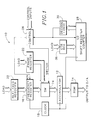
- a direct digital synthesizer 10 has an accumulator 12 that generates addresses for a memory 14.
- a frequency register 16 provides an index, being either an integer or fractional value, that is added to the accumulator 12 for each cycle of a clock signal from an internal clock 18.
- a next frequency register 20 contains an index value for a new frequency to be loaded into the frequency register 16 when a frequency change is to be implemented.
- a phase register 22 is preloaded with a phase jump value and coupled to the accumulator 12 via a switch 24. The switch 24 normally couples the frequency register 16 to the accumulator except for one clock cycle when a phase change is to be implemented.
- a logic control circuit 26 provides an enable signal to the frequency register 16 when a frequency change, as indicated by control inputs to the logic control circuit, is desired so that on one phase of the next clock cycle the contents of the next frequency register 20 are loaded into the frequency register 16.
- the logic control circuit 26 also provides a switch signal to the switch 24 which causes the switch to couple the output of the phase register 22 to the accumulator 12 when a phase change is desired.
- the next frequency register 20 and phase register 22 are loaded by the logic control circuit 26 according to parameters contained in the control inputs, which parameters include what type of change and the register values for the change.
- the present invention adds to the DDS 10 described above a feedback linear shift register counter 28 so that the frequency and phase changes can be made at the internal clock rate rather than being dependent upon external clock rates as in the prior art.
- the shift register 28 is loaded with an initial count by the logic control circuit 26 from a counter register 36 at the end of its count cycle as generated by the decode logic 30. The load is accomplished on the regular phase of a single internal clock cycle. At the next clock the shift register 28 shifts.
- the outputs of the shift stages that make up the shift register 28 are input to a decode logic circuit 30 that looks for an "end-of-count" condition.
- a signal is sent to the logic control circuit 26 either to enable the frequency register 16 for loading a new index value from the next frequency register 20 during one phase of the clock cycle prior to adding to the accumulator 12, or to switch the input to the accumulator via the switch 24 to the phase register 22 so that a phase jump occurs on the next accumulator addition, or both.
- the end-of-count also reloads the shift register counter 28 from the counter register 36.
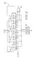
- the shift register 28 as shown in greater detail in Fig. 2, has a plurality of single-bit shift stages 32 coupled in series. On one edge of the clock cycle the data at the input of each stage 32 is clocked into that stage so that the contents of the shift register 26 are shifted simultaneously one bit to the right.
- the outputs from at least two of the stages 32 are input to an exclusive OR gate 34 to provide a feedback input value to the first stage of the shift register 26. The result is that after a predetermined number of clock cycles a predetermined output from the shift register occurs that is detected by the decode logic circuit.
- the initial count value that is preloaded into the shift register 28 from the counter register 36 is obtained from a lookup table that has a plurality of initial count values corresponding to a plurality of desired time delays since, unlike a conventional up/down counter, the count from an initial count to a final end-of-count value is not directly ascertainable. Also note that the value loaded into the shift register 28 shown in Fig. 2 has to be non-zero, since a zero value does not cause the contents of the shift register to change as the zero is constantly recirculated through the register.
- the count progresses as follows: 0111111, 0011111, 0001111, 0000111, 0000011, 0000001, 1000000, 0100000, ... , 0000010, 1000001, etc.
- a shift register is used as a counter instead of a conventional counter due to the time delay between the change of the least significant bit to the change of the most significant bit in a conventional counter.
- the feedback propagation delay of the shift register 28 is independent of the number of stages, or length, of the shift register. Also with the proper selection of the stage 32 outputs to be fed back, counts as high as 2-n-1 can be achieved, only one count less than for a binary counter of n bits.
- the present invention provides a direct digital synthesizer (DDS) with a feedback shift register configured as a counter to provide switch signals to a logic controller in order to implement frequency/phase changes at the rate of the reference clock internal to the DDS.
- DDS direct digital synthesizer
- This integration of the accumulator 12 of the DDS 10 and the shift register 28 allows for the ability to change the signal characteristics from the DDS at a precise instant of time, such as for generation of spread spectrum communication signals, including direct sequence phase modulation or frequency hopping modulation.
Landscapes
- Engineering & Computer Science (AREA)
- Theoretical Computer Science (AREA)
- Physics & Mathematics (AREA)
- General Engineering & Computer Science (AREA)
- General Physics & Mathematics (AREA)
- Stabilization Of Oscillater, Synchronisation, Frequency Synthesizers (AREA)
Applications Claiming Priority (2)
| Application Number | Priority Date | Filing Date | Title |
|---|---|---|---|
| US61576890A | 1990-11-19 | 1990-11-19 | |
| US615768 | 1990-11-19 |
Publications (2)
| Publication Number | Publication Date |
|---|---|
| EP0486851A2 true EP0486851A2 (de) | 1992-05-27 |
| EP0486851A3 EP0486851A3 (en) | 1993-04-07 |
Family
ID=24466730
Family Applications (1)
| Application Number | Title | Priority Date | Filing Date |
|---|---|---|---|
| EP19910118419 Withdrawn EP0486851A3 (en) | 1990-11-19 | 1991-10-29 | Direct digital synthesizer with feedback shift register |
Country Status (2)
| Country | Link |
|---|---|
| EP (1) | EP0486851A3 (de) |
| JP (1) | JPH0555832A (de) |
Cited By (2)
| Publication number | Priority date | Publication date | Assignee | Title |
|---|---|---|---|---|
| EP0599663A2 (de) * | 1992-11-27 | 1994-06-01 | Samsung Electronics Co., Ltd. | Chrominanzsignalverarbeitung |
| WO2004079885A2 (en) * | 2003-03-06 | 2004-09-16 | Aeroflex International Limited | Improved waveform generation |
Citations (4)
| Publication number | Priority date | Publication date | Assignee | Title |
|---|---|---|---|---|
| US3866022A (en) * | 1972-12-26 | 1975-02-11 | Nasa | System for generating timing and control signals |
| JPS5799007A (en) * | 1980-12-12 | 1982-06-19 | Fujitsu Ltd | Voltage controlled variable frequency oscillator |
| EP0312370A2 (de) * | 1987-10-13 | 1989-04-19 | Matsushita Electric Industrial Co., Ltd. | Digitaloszillator |
| US4956798A (en) * | 1989-08-03 | 1990-09-11 | Tektronix, Inc. | Arbitrary waveform generator with adjustable spacing |
Family Cites Families (2)
| Publication number | Priority date | Publication date | Assignee | Title |
|---|---|---|---|---|
| JPS58172004A (ja) * | 1982-04-26 | 1983-10-08 | テクトロニクス・インコ−ポレイテツド | デジタル信号発生装置 |
| JPS6471304A (en) * | 1987-09-11 | 1989-03-16 | Yokogawa Electric Corp | Sweep oscillator |
-
1991
- 1991-10-29 EP EP19910118419 patent/EP0486851A3/en not_active Withdrawn
- 1991-11-19 JP JP3330085A patent/JPH0555832A/ja active Pending
Patent Citations (4)
| Publication number | Priority date | Publication date | Assignee | Title |
|---|---|---|---|---|
| US3866022A (en) * | 1972-12-26 | 1975-02-11 | Nasa | System for generating timing and control signals |
| JPS5799007A (en) * | 1980-12-12 | 1982-06-19 | Fujitsu Ltd | Voltage controlled variable frequency oscillator |
| EP0312370A2 (de) * | 1987-10-13 | 1989-04-19 | Matsushita Electric Industrial Co., Ltd. | Digitaloszillator |
| US4956798A (en) * | 1989-08-03 | 1990-09-11 | Tektronix, Inc. | Arbitrary waveform generator with adjustable spacing |
Non-Patent Citations (1)
| Title |
|---|
| PATENT ABSTRACTS OF JAPAN vol. 6, no. 185 (E-132) & JP-A-57 099 007 ( FUJITSI ) 19 June 1982 * |
Cited By (5)
| Publication number | Priority date | Publication date | Assignee | Title |
|---|---|---|---|---|
| EP0599663A2 (de) * | 1992-11-27 | 1994-06-01 | Samsung Electronics Co., Ltd. | Chrominanzsignalverarbeitung |
| EP0599663A3 (de) * | 1992-11-27 | 1995-01-18 | Samsung Electronics Co Ltd | Chrominanzsignalverarbeitung. |
| WO2004079885A2 (en) * | 2003-03-06 | 2004-09-16 | Aeroflex International Limited | Improved waveform generation |
| WO2004079885A3 (en) * | 2003-03-06 | 2004-10-28 | Aeroflex Internat Ltd | Improved waveform generation |
| US7702707B2 (en) | 2003-03-06 | 2010-04-20 | Aeroflex International Limited | Waveform generation |
Also Published As
| Publication number | Publication date |
|---|---|
| JPH0555832A (ja) | 1993-03-05 |
| EP0486851A3 (en) | 1993-04-07 |
Similar Documents
| Publication | Publication Date | Title |
|---|---|---|
| US5361290A (en) | Clock generating circuit for use in single chip microcomputer | |
| US4853653A (en) | Multiple input clock selector | |
| US6518813B1 (en) | Clock generating circuit and semiconductor integrated circuit using the same | |
| US5459855A (en) | Frequency ratio detector for determining fixed frequency ratios in a computer system | |
| US10523211B2 (en) | Wide range glitchless switchable clock divider with modified 2/3 divider stages | |
| US5789953A (en) | Clock signal generator providing non-integer frequency multiplication | |
| US6501816B1 (en) | Fully programmable multimodulus prescaler | |
| US5638017A (en) | Pulse width modulation circuit | |
| US5144571A (en) | Direct digital synthesizer with feedback shift register | |
| KR20020049387A (ko) | 고속 동작이 가능하고 순차적으로 2진 카운터 순서를 갖는카운터 회로 및 그 카운팅 방법 | |
| US6795932B2 (en) | Clock switchover circuit | |
| US4234849A (en) | Programmable frequency divider and method | |
| US5355462A (en) | Processor data memory address generator | |
| KR100239430B1 (ko) | 가변 비정수배 분주회로 | |
| EP0486851A2 (de) | Direkter digitaler Synthetisierer mit rückgekoppeltem Schieberegister | |
| US6157267A (en) | Variable frequency multiple loop ring oscillator | |
| US20030058004A1 (en) | Method and apparatus for direct digital synthesis of frequency signals | |
| US4759042A (en) | Parallel-to-serial converter | |
| US10749530B1 (en) | Programmable divider with glitch-free load circuit | |
| JPH1198007A (ja) | 分周回路 | |
| US5521952A (en) | Pulse counter circuit and pulse signal changeover circuit therefor | |
| JPH0991982A (ja) | シフトレジスタ | |
| KR100261183B1 (ko) | 계수기 | |
| KR940000223B1 (ko) | 고정밀 펄스폭 변조회로 | |
| KR100193998B1 (ko) | 고정밀 디지탈 분주회로 |
Legal Events
| Date | Code | Title | Description |
|---|---|---|---|
| PUAI | Public reference made under article 153(3) epc to a published international application that has entered the european phase |
Free format text: ORIGINAL CODE: 0009012 |
|
| AK | Designated contracting states |
Kind code of ref document: A2 Designated state(s): DE FR GB NL |
|
| PUAL | Search report despatched |
Free format text: ORIGINAL CODE: 0009013 |
|
| AK | Designated contracting states |
Kind code of ref document: A3 Designated state(s): DE FR GB NL |
|
| 17P | Request for examination filed |
Effective date: 19930630 |
|
| 17Q | First examination report despatched |
Effective date: 19950825 |
|
| STAA | Information on the status of an ep patent application or granted ep patent |
Free format text: STATUS: THE APPLICATION IS DEEMED TO BE WITHDRAWN |
|
| 18D | Application deemed to be withdrawn |
Effective date: 19960105 |