EP0484013A2 - Verfahren zur Herstellung einer integrierten Schaltung - Google Patents
Verfahren zur Herstellung einer integrierten Schaltung Download PDFInfo
- Publication number
- EP0484013A2 EP0484013A2 EP91309610A EP91309610A EP0484013A2 EP 0484013 A2 EP0484013 A2 EP 0484013A2 EP 91309610 A EP91309610 A EP 91309610A EP 91309610 A EP91309610 A EP 91309610A EP 0484013 A2 EP0484013 A2 EP 0484013A2
- Authority
- EP
- European Patent Office
- Prior art keywords
- noise
- film
- test portion
- spectrum
- steps
- Prior art date
- Legal status (The legal status is an assumption and is not a legal conclusion. Google has not performed a legal analysis and makes no representation as to the accuracy of the status listed.)
- Withdrawn
Links
Images
Classifications
-
- G—PHYSICS
- G01—MEASURING; TESTING
- G01R—MEASURING ELECTRIC VARIABLES; MEASURING MAGNETIC VARIABLES
- G01R31/00—Arrangements for testing electric properties; Arrangements for locating electric faults; Arrangements for electrical testing characterised by what is being tested not provided for elsewhere
- G01R31/28—Testing of electronic circuits, e.g. by signal tracer
- G01R31/2851—Testing of integrated circuits [IC]
- G01R31/2855—Environmental, reliability or burn-in testing
- G01R31/2856—Internal circuit aspects, e.g. built-in test features; Test chips; Measuring material aspects, e.g. electro migration [EM]
- G01R31/2858—Measuring of material aspects, e.g. electro-migration [EM], hot carrier injection
-
- G—PHYSICS
- G01—MEASURING; TESTING
- G01R—MEASURING ELECTRIC VARIABLES; MEASURING MAGNETIC VARIABLES
- G01R31/00—Arrangements for testing electric properties; Arrangements for locating electric faults; Arrangements for electrical testing characterised by what is being tested not provided for elsewhere
- G01R31/26—Testing of individual semiconductor devices
- G01R31/27—Testing of devices without physical removal from the circuit of which they form part, e.g. compensating for effects surrounding elements
- G01R31/275—Testing of devices without physical removal from the circuit of which they form part, e.g. compensating for effects surrounding elements for testing individual semiconductor components within integrated circuits
-
- H—ELECTRICITY
- H10—SEMICONDUCTOR DEVICES; ELECTRIC SOLID-STATE DEVICES NOT OTHERWISE PROVIDED FOR
- H10P—GENERIC PROCESSES OR APPARATUS FOR THE MANUFACTURE OR TREATMENT OF DEVICES COVERED BY CLASS H10
- H10P74/00—Testing or measuring during manufacture or treatment of wafers, substrates or devices
- H10P74/23—Testing or measuring during manufacture or treatment of wafers, substrates or devices characterised by multiple measurements, corrections, marking or sorting processes
-
- G—PHYSICS
- G01—MEASURING; TESTING
- G01R—MEASURING ELECTRIC VARIABLES; MEASURING MAGNETIC VARIABLES
- G01R31/00—Arrangements for testing electric properties; Arrangements for locating electric faults; Arrangements for electrical testing characterised by what is being tested not provided for elsewhere
- G01R31/28—Testing of electronic circuits, e.g. by signal tracer
- G01R31/2851—Testing of integrated circuits [IC]
- G01R31/2855—Environmental, reliability or burn-in testing
- G01R31/2856—Internal circuit aspects, e.g. built-in test features; Test chips; Measuring material aspects, e.g. electro migration [EM]
Definitions
- This invention pertains to methods for the manufacture of integrated circuits, and in particular to methods including the reliability testing of metal films that are included in such circuits.
- Electromigration is the mass transport of ions along a metal conductor as a result of a large electron current density in the conductor and is generally an undesirable phenomenon.
- the typical mechanism for electromigration damage to metallization lines in integrated circuits (ICs) is believed to be a two-stage process.
- mass transport of conductor atoms results in the thinning of the conductor in some areas (for example, void formation), and the thickening of the conductor in other areas (for example, hillock formation).
- the second stage either the voids grow large enough to interrupt the flow of current, causing an open circuit, or the hillocks grow out toward a neighboring metallization line, causing a short circuit.
- MTF Median Time to Failure
- TRACE Temporal Ramp Resistance Analysis to Characterize Electromigration
- a particularly useful Wheatstone bridge method is described by J. H. Scofield, "AC Method for Measuring Low-Frequency Resistance Fluctuation Spectra,” Rev. Sci. Instrum. , Vol. 58, pp. 985-993 (1987).
- the Scofield method makes use of a center-tapped four-point probe for contacting the sample. That is, the sample resistance is divided into two equal portions by the center tap of the probe. Thus, the sample comprises not one, but two arms of a Wheatstone bridge.
- two or more resistors which comprise at least one ballast resistor and at least one measuring resistor
- the voltage source which applies a voltage signal having an ac component
- the ac component of the bridge imbalance signal appearing across a portion of the sample is amplified and demodulated by a phase sensitive amplifier.
- this measurement technique is relatively insensitive to fluctuations in the source voltage.
- the amplifier can be used near its optimum frequency, and the use of phase sensitive detection is very effective in excluding background noise.
- Scofield discusses the use of this technique for measuring resistance fluctuations in metal films. Scofield also mentions that for certain purposes it may be useful to apply a source voltage having both ac and dc components Scofield does not, however, discuss any application of this technique for investigating phenomena related to electromigration, and in particular, he does not suggest the use of the dc component for stimulating electromigration. Moreover, the metal film samples discussed by Scofield were wirebonded to a 24-pin IC package prior to the measurements. However, the steps involved in wirebonding introduce a significant time delay between preparation of the films and their measurement. Such delay may be undesirable in applications of the measurement technique for the diagnosis of processes on an IC production line.
- the invention is a method for manufacturing an integrated circuit which includes the steps of providing one or more semiconductor substrates (here referred to as "wafers") to be processed, and processing them. During the processing, a patterned metallic film including at least one strip-like test portion is formed on each of at least some of the substrates. The test portions are formed in addition to, or (on selected wafers) in place of, the metallized regions that are intended to be incorporated in ICs.
- the method further includes the step of evaluating a film test portion on at least one of the substrates relative to predetermined standards. If the result of the evaluation so indicates, the method further includes adjusting one or more process parameters such that subsequently processed substrates include film test portions conforming to the predetermined standards.
- the method optionally further includes performing one or more additional steps toward formation of the integrated circuit.
- the evaluating step comprises: causing a direct current and an alternating current to flow in the test portion, the combined currents being of sufficient magnitude to stimulate 1/f2 noise in the test portion; determining the noise spectrum associated with the alternating current; and comparing the slope and amplitude of the spectrum with predetermined values at one or more preselected frequencies.
- each test portion is appropriately patterned for incorporation in a Wheatstone bridge by means of a center-tapped four-point probe apparatus, as described, for example, in Scofield, cited above.
- each test portion to be incorporated includes five contact regions (sometimes referred to as "contact pads").
- five point contacts are provided on the probe, each of which is to be applied to one of the five contact pads.
- a signal is applied to the bridge, typically consisting of a dc current component of relatively large amplitude, to which an ac current component of relatively small amplitude is added.
- the dc component stimulates electromigration in the sample, whereas the ac component is preferably made small enough to have negligible effect on electromigration.
- the ac component of the voltage drop across the sample film is modulated by resistance fluctuations in the sample. The modulation appears in an imbalance signal across the output terminals of the bridge.
- the imbalance signal is amplified, demodulated, and detected using a phase sensitive amplifier such as a lock-in amplifier.
- the output of the phase sensitive amplifier represents the noise signal.
- the noise signal is processed by a spectrum analyzer to produce a noise power spectrum.
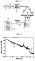
- FIG. 1 is a schematic block diagram of an exemplary test configuration for practicing the inventive method.
- FIG. 2 is a typical noise power spectrum of a metal film to which a dc current is applied to stimulate electromigration.
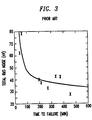
- FIG. 3 is an exemplary graph, taken from the prior art, depicting a correlation between time to failure of metal films and noise in those films.
- At least one IC is conventionally fabricated on each of one or more wafers, typically semiconductor wafers or wafers of other suitable substrate material for semiconductor-based electronic components.
- at least one test structure is also formed on at least one of the wafers.
- a multiplicity of ICs are formed in a rectangular grid pattern on the surface of a wafer.
- the test structure or structures are formed on portions of the wafer that are not occupied by ICs. It is preferable to form test structures within the grid pattern, in the spaces (ie, the "kerf" areas) between ICs.
- Each test structure comprises a metal film patterned to accommodate the contact points of a probing apparatus that makes electrical contact with the test structure by the application of pressure between the contact points and the test structure. Enough pressure is typically exerted between the probe and the sample (i.e., the metal film) to leave a mark (referred to as a "footprint") on the sample at each point of contact.
- the test structure is patterned to provide five pads for contact with a center-tapped four-point probe Each pad is exemplarily a square having an edge length of 75-100 ⁇ m.
- one or more wafers are selected for reliability testing. The results of such testing are useful for setting the parameters of the metallization process being performed in the relevant manufacturing line.
- the deposition temperature affects grain size, as is well known in the art.
- Another such parameter is the residual gas pressure in the deposition chamber because, for example, residual oxygen that may be present may migrate to the grain boundaries and weaken them.
- Yet another parameter is the purity of the metal target that is the source of the metal being deposited.
- certain characteristics of the lithographic process by which the metal layer is patterned are capable of affecting reliability. For example, when chlorine is used as a reactive-ion etchant, chlorine residues can lead to corrosion of the metal film. Thus, for example, measures designed to decrease or eliminate corrosive residues can be taken in response to the results of reliability testing.
- the point contacts are exemplarily sharpened to a diameter of 20-40 ⁇ m at the tip, and are exemplarily spaced with a pitch that is twice the edge length of a contact pad.
- Point contact 5 is electrically connected to ground via a connection external to the film
- Point contacts 1 and 2 located at opposite ends of the film, connect the film to the output terminal of constant current amplifier 8 via a resistive network comprising resistors 9, 10, and 11. That is, the film, as viewed in the figure, is divided into a left half and a right half by point contact 5. Electric current flows from amplifier 8 through resistor 9, and into the left half of film 20 via point contact 1, and returns to amplifier 8 through ground via point contact 5.
- the film, together with resistors 9, 10, and 11, thus forms a Wheatstone bridge connected across the output terminal and the ground terminal of amplifier 8.
- the left arm of the bridge comprises resistor 9 and the left half of the film.
- the right arm of the bridge comprises resistors 10 and 11, and the right half of the film.
- resistors 9 and 10 are ballast resistors, each having a resistance of about 200 ⁇ . To keep them at a constant temperature, they advantageously are heat-sinked and water-cooled.
- Resistor 11 is, exemplarily, a wire-wound variable resistor having a maximum resistance of about 100 ⁇ . The maximum ac current flowing in the bridge is typically about 100 ma.
- the output of amplifier 8 consists of a current that is proportional to the voltage signal applied between ground and the input terminal of the amplifier.
- the voltage signal is provided by dc voltage source 6 and ac voltage source 7 operating in series.
- the input voltage signal, and the output current have stable waveforms and do not substantially contribute background noise (i.e., noise that is unrelated to electromigration or other processes inherent in the film to be tested) to the measurement system.
- the frequency of the ac voltage signal is selected to be within the optimum frequency range for amplification by preamplifier 14, and also relatively far from the frequencies characterizing mechanical vibrations in the manufacturing environment.
- the ac frequency is desirably at least about ten times the highest frequency that is expected to make a significant contribution to the noise power spectrum associated with electromigration.
- a useful range of frequencies is 10 Hz-103 Hz.
- a preferred value for the ac frequency is about 200 Hz, which is about 20 times the highest frequency of interest in the noise spectrum, as explained below.
- the frequencies associated with mechanical noise in the relevant manufacturing environment typically occupy the range from about 1 Hz to about 10 Hz.
- the frequencies of interest in the noise power spectrum obtained by the inventive method are also approximately in the range 1-10 Hz. That is, the time required for spectrum analyzer 16 to calculate the noise power associated with frequencies below about 1 Hz is undesirably long, and extending the spectrum into that range is of limited additional value. Therefore, noise power below about 1 Hz is not typically analyzed. As a practical matter, at frequencies above about 10 Hz, that component of the noise power that is due to electromigration generally tends to be buried in the thermal noise component. Therefore, noise power above about 10 Hz is also typically not analyzed.
- Point contact 3 is electrically connected to the left half of the film at a point intermediate point contacts 1 and 5.
- Point contact 4 is electrically connected to the right half of the film at a point intermediate point contacts 2 and 5. Because the current in the resistive network has both an ac and a dc component, the voltage difference between point contacts 3 and 4 generally also has an ac and a dc component. The ac component of this voltage difference is inductively coupled, via isolation transformer 13, to preamplifier 14. Direct current is excluded from the transformer primary circuit by capacitor 12.
- the preamplified signal is fed to lock-in amplifier 15, which is frequency and phase locked to the signal.
- the lock-in amplifier amplifies and demodulates the ac signal, providing an output signal that is slowly varying relative to the ac frequency.
- This output signal is fed to spectrum analyzer 16, which exemplarily performs a fast Fourier transform on the signal to determine its spectral power density which is, for example, displayed as a function of frequency on a suitable output device. All these components
- a conventional low-pass filter (not shown) having a cut-off at, for example, 20 Hz is optionally included in the measuring circuit at a point between lock-in amplifier 15 and spectrum analyzer 16.
- the resistive network forms a Wheatstone bridge.
- the bridge can be nulled to an applied ac signal. That is, with alternating current flowing out of amplifier 8 and through the two sides of the bridge, the amplitude of the ac voltage drop between point contacts 3 and 4 is brought essentially to zero (except for relatively low-amplitude noise, to be discussed below).
- the bridge is nulled automatically. That is, the ac bridge imbalance voltage is amplified, for example, by preamplifier 14 and amplified and demodulated by lock-in amplifier 15, and the resulting dc signal is sensed at the output of the lock-in amplifier. Under the control of an appropriately programmed microprocessor, the resistance of resistor 11 is varied, and the phase of lock-in amplifier 15 is adjusted, to minimize the imbalance voltage. This procedure is repeated each time the sample is changed, and each time a measurement variable (such as temperature or bridge current) is changed.
- a measurement variable such as temperature or bridge current
- the bridge When the bridge is nulled and an appropriately large dc current is flowing, most of the noise voltage appearing between point contacts 3 and 4 is caused by resistance fluctuations related to electromigration in the left and right sides of the film.
- the voltage drop v34 between point contacts 3 and 4 includes an ac component that is modulated by the same resistance fluctuations.
- the alternating current preferably has a relatively small amplitude, such that it has essentially negligible effect on the electromigration process.
- Information about electromigration is provided, as discussed above, by amplifying, demodulating, and spectrally analyzing the ac component of v34.
- Two aspects of this measurement technique are effective in excluding background noise arising from sources external to the film (in distinction, e.g., to electromigration noise); they are the bridge geometry and the use of phase-sensitive detection. That is, the lock-in amplifier is effective for excluding noise arising as a result of mechanical vibration, because a signal frequency can be chosen that is far from any frequencies characteristic of mechanical vibrations in the manufacturing environment.
- the bridge is made relatively insensitive to contact noise by choosing values of the external resistors (i.e., resistors 9, 10, and 11) that are much greater than the contact resistance fluctuations associated with contact noise. Such a choice assures that the current flowing in the film will be relatively insensitive to the relatively small resistance fluctuations at point contacts 1 and 2.
- the noise voltage v34 is insensitive to contact noise at point contact 5 because contact noise at that point changes the voltages at contacts 3 and 4 in step such that their difference is essentially unaffected.
- the output of spectrum analyzer 16 is a noise power density spectrum, typically extending from about 1 Hz to about 10 Hz, as discussed above.
- the spectrum typically exhibits two portions, a low-frequency portion A and a high-frequency portion B, generally separated by a transition region.
- Portion A corresponding to the frequency range where electromigration is the dominant source of noise, bears an inverse-square relation to the frequency. (That is, letting f represent frequency, the noise power spectral density is proportional to f - ⁇ , where ⁇ is approximately equal to 2.)
- Portion B may be dominated by thermal noise (at least in a certain frequency range), which typically produces a noise power density spectrum that is relatively flat with respect to frequency.
- Portion B may also be dominated by 1/f noise (at least in a certain frequency range), or by a combination of 1/f and thermal noise (It should be noted in this regard that the spectrum of FIG. 2 includes the effects of a low-pass filter having a cut-off at 20 Hz, included in the measuring circuit as discussed above. The low-pass filter caused a sharp roll-off to appear in the spectrum between 20 Hz and 30 Hz.)
- portion A (and possibly also portion B) appears as an approximate straight line.
- the slope of portion A is - ⁇ (where ⁇ is equal to approximately 2), or (according to the manner of labeling the axes of FIG. 2) approximately 20 dB per decade.
- the noise spectrum is readily compared with predetermined criteria in order to evaluate the reliability of the metal film (and by inference, the reliability of other metal films formed under substantially identical conditions). Such information can provide a basis for adjusting process parameters to improve the reliability of the metal films being formed, e.g., metal films that are to be incorporated in ICs. In addition, comparisons between spectra taken from films formed on multiple wafers processed in a single manufacturing line are useful for assessing the consistency of the film-forming process.
- the criteria for determining the reliability of the metallization are at least partly dependent on the manufacturing line. That is, reliability depends, inter alia, on the composition of the metal film and its grain structure.
- IC metallization is conventionally aluminum based
- various alloys of aluminum may be employed. Wherereas some manufacturing lines use pure aluminium, others use alloys containing a few percent copper and/or silicon, while still others use aluminium alloys containing titanium or palladium for forming at least a portion of an IC metallization pattern.
- the grain structure of the film is itself dependent on process parameters. A film formed, for example, by a process producing relatively small grains may be more susceptible to electromigration damage than a film of the same composition formed by a process producing relatively large grains.
- S f (e.g., S 1 Hz ) is readily compared with predetermined criteria. That is, the magnitude of the 1/f2 noise is readily correlated to the results of conventional reliability tests such as MTF tests (although, as noted, correlations are valid, in general, only for films of comparable compositions and grain structures).
- MTF tests although, as noted, correlations are valid, in general, only for films of comparable compositions and grain structures.
- Cottle and Chen (1987), cited above presents a graphical plot of the total RMS noise in aluminum films against the time to failure of the films. That plot is reproduced here as FIG. 3.
- the inventive testing method is readily applied at any point dig the manufacture of an IC, provided a metal test pattern has been formed and is accessible to probes (i.e., it has not been removed or covered over).
- the method is preferably applied immediately after the patterning of a metallization layer (the patterned layer to include an appropriate test pattern).
- the inventive method is readily repeated for each such layer.
- steps in the manufacture of the IC are conventional, and are readily apparent to the practitioner of ordinary skill.
- steps might include, after providing a substrate wafer, the steps of growing at least one oxide layer on the wafer, patterning at least one oxide layer, and doping selected portions of the substrate.
- one or more metallized layers may be formed and patterned.
- the wafer may be divided into portions, each corresponding to an individual IC, electrical leads may be attached to the portions, and each portion may be encapsulated to form a packaged IC.
- An aluminum film containing 0.5% copper was deposited on a silicon substrate.
- the film thickness was 0.5 ⁇ m, and the film was patterned into a strip 075 ⁇ m wide.
- the film was incorporated in a Wheatstone bridge by means of a center tapped, four-point probe, as described above.
- a current density of 34 x 107 A/cm2 was passed through the film.
- the temperature of the film was uncontrolled, and the passage of current raised the film temperature to a maximum of about 45°C.
- the noise spectrum was measured by lock-in amplification and demodulation of the bridge imbalance signal followed by fast-Fourier-transform spectral analysis, as described above.
- the measured value of ⁇ was 2.08.
- the threshold current density at which a changed from about 1 to about 2 was observed to be about 1.5 x 10⁷ A/cm2.
- the rms noise voltage at 1 Hz was found to be about 4.6 x 10 ⁇ 8 V.
Landscapes
- Engineering & Computer Science (AREA)
- Microelectronics & Electronic Packaging (AREA)
- Physics & Mathematics (AREA)
- General Physics & Mathematics (AREA)
- Environmental & Geological Engineering (AREA)
- Computer Hardware Design (AREA)
- General Engineering & Computer Science (AREA)
- Testing Or Measuring Of Semiconductors Or The Like (AREA)
Applications Claiming Priority (2)
| Application Number | Priority Date | Filing Date | Title |
|---|---|---|---|
| US605043 | 1990-10-29 | ||
| US07/605,043 US5057441A (en) | 1990-10-29 | 1990-10-29 | Method for reliability testing integrated circuit metal films |
Publications (2)
| Publication Number | Publication Date |
|---|---|
| EP0484013A2 true EP0484013A2 (de) | 1992-05-06 |
| EP0484013A3 EP0484013A3 (en) | 1993-05-26 |
Family
ID=24422031
Family Applications (1)
| Application Number | Title | Priority Date | Filing Date |
|---|---|---|---|
| EP19910309610 Withdrawn EP0484013A3 (en) | 1990-10-29 | 1991-10-17 | Method for manufacturing an integrated circuit |
Country Status (3)
| Country | Link |
|---|---|
| US (1) | US5057441A (de) |
| EP (1) | EP0484013A3 (de) |
| JP (1) | JPH04298058A (de) |
Cited By (3)
| Publication number | Priority date | Publication date | Assignee | Title |
|---|---|---|---|---|
| EP0599763A1 (de) * | 1992-11-02 | 1994-06-01 | International Business Machines Corporation | Zweikanalige, rauscharme DC-Messanordnung und Testverfahren |
| US5514974A (en) * | 1994-10-12 | 1996-05-07 | International Business Machines Corporation | Test device and method for signalling metal failure of semiconductor wafer |
| WO2001080305A3 (en) * | 2000-04-17 | 2002-03-21 | Univ Texas | Electromigration early failure distribution in submicron interconnects |
Families Citing this family (26)
| Publication number | Priority date | Publication date | Assignee | Title |
|---|---|---|---|---|
| US5798649A (en) * | 1991-12-26 | 1998-08-25 | Texas Instruments Incorporated | Method for detecting defects in semiconductor insulators |
| US5504434A (en) * | 1992-12-18 | 1996-04-02 | International Business Machines Corporation | Instrument for the measurement of electrical characteristics during manufacturing processes |
| US5598102A (en) * | 1993-08-19 | 1997-01-28 | Texas Instruments Incorporated | Method for detecting defects in semiconductor insulators |
| JPH07130817A (ja) * | 1993-10-30 | 1995-05-19 | Sony Corp | 金属配線の信頼性評価方法及び金属配線の信頼性評価装置 |
| US5625288A (en) * | 1993-10-22 | 1997-04-29 | Sandia Corporation | On-clip high frequency reliability and failure test structures |
| US5723874A (en) * | 1996-06-24 | 1998-03-03 | International Business Machines Corporation | Dishing and erosion monitor structure for damascene metal processing |
| US6043662A (en) * | 1996-09-18 | 2000-03-28 | Alers; Glenn Baldwin | Detecting defects in integrated circuits |
| DE19722077B4 (de) * | 1997-05-27 | 2006-11-16 | Horiba Automotive Test Systems Gmbh | Trägerfrequenzmeßverfahren |
| US5970429A (en) * | 1997-08-08 | 1999-10-19 | Lucent Technologies, Inc. | Method and apparatus for measuring electrical noise in devices |
| US6255707B1 (en) | 1998-08-24 | 2001-07-03 | Lucent Technologies, Inc. | Semiconductor laser reliability test structure and method |
| JP3164106B2 (ja) * | 1999-06-29 | 2001-05-08 | 日本電気株式会社 | 集積回路の故障検出方法及び故障検出装置及びその制御プログラムを記録した記憶媒体 |
| JP2001257672A (ja) | 2000-03-14 | 2001-09-21 | Mitsubishi Electric Corp | 認証方法、認証装置、認証システム、および、icカード |
| JP2002033362A (ja) * | 2000-07-17 | 2002-01-31 | Matsushita Electric Ind Co Ltd | 半導体検査装置 |
| US6747471B1 (en) | 2002-01-10 | 2004-06-08 | Taiwan Semiconductor Manufacturing Company | Method and apparatus to estimate burn-in time by measurement of scribe-line devices, with stacking devices, and with common pads |
| US6995392B2 (en) * | 2002-08-07 | 2006-02-07 | International Business Machines Corporation | Test structure for locating electromigration voids in dual damascene interconnects |
| US7332360B2 (en) * | 2004-10-25 | 2008-02-19 | Applied Materials, Inc. | Early detection of metal wiring reliability using a noise spectrum |
| US7151010B2 (en) * | 2004-12-01 | 2006-12-19 | Kyocera Wireless Corp. | Methods for assembling a stack package for high density integrated circuits |
| US7217994B2 (en) * | 2004-12-01 | 2007-05-15 | Kyocera Wireless Corp. | Stack package for high density integrated circuits |
| JP2007040771A (ja) * | 2005-08-02 | 2007-02-15 | Nec Electronics Corp | ノイズ測定用半導体装置 |
| CN101295002B (zh) * | 2007-04-24 | 2010-09-29 | 中芯国际集成电路制造(上海)有限公司 | 互连线失效检测方法 |
| CN102788911B (zh) * | 2012-09-06 | 2015-07-22 | 电子科技大学 | 一种热敏薄膜噪声测试方法 |
| JP6056806B2 (ja) * | 2014-05-13 | 2017-01-11 | 信越半導体株式会社 | 半導体基板の評価方法 |
| US9817063B2 (en) | 2016-02-19 | 2017-11-14 | Globalfoundries Inc. | Interconnect reliability structures |
| US10161994B2 (en) * | 2016-06-14 | 2018-12-25 | Formfactor Beaverton, Inc. | Systems and methods for electrically testing electromigration in an electromigration test structure |
| US11448692B2 (en) * | 2018-08-16 | 2022-09-20 | Taiwann Semiconductor Manufacturing Company Ltd. | Method and device for wafer-level testing |
| US11073551B2 (en) * | 2018-08-16 | 2021-07-27 | Taiwan Semiconductor Manufacturing Company Ltd. | Method and system for wafer-level testing |
-
1990
- 1990-10-29 US US07/605,043 patent/US5057441A/en not_active Expired - Lifetime
-
1991
- 1991-10-17 EP EP19910309610 patent/EP0484013A3/en not_active Withdrawn
- 1991-10-29 JP JP3281778A patent/JPH04298058A/ja not_active Withdrawn
Non-Patent Citations (6)
| Title |
|---|
| 23rd annual proceedings reliability physics 1985, Orlando,Florida,March 26-28, 1985,IEEE Cat.nr. 85CH2113-9,pp.100-107, B.J. ROOT et all.:"Wafer Level Electro migration Tests for Production Monitoring" * |
| 26th annual proceedings reliability physics 1988, Monterey, California, April 12-14, 1988, IEEE Cat.nr. CH2508-88, pp.203-208, J.G. COTTLE et al.:"A Compa rison between Noise Measurements and Conventional Electromigration Reliability Testing" * |
| APPLIED PHYSICS LETTERS. vol. 23, no. 6, 15 September 1973, NEW YORK US pages 287 - 289 J.L. VOSSEN 'Screening of Metal Film Defects by Current Noise Measurement' * |
| REVIEW OF SCIENTIFIC INSTRUMENTS vol. 58, no. 6, June 1987, NEW YORK US pages 985 - 993 J.H. SCOTFIELD 'Ac Method for Measuring Low-Frequency Resistance Fluctuation Spectra' * |
| SOLID STATE ELECTRONICS. vol. 32, no. 1, 1989, OXFORD GB pages 11 - 16 A. DILIGENTI ET AL. 'A Study of Electromigration in Aluminum and Aluminum-Silicon Thin Film Resistors Using Noise Technique' * |
| Test Technology Committee, Curriculum for Test Technology, 1983, pp.37-40, IEEE Cat.nr. CH1978-6/83, A. PECZALSKI :"Noise Measurements as a Testing Tool" * |
Cited By (4)
| Publication number | Priority date | Publication date | Assignee | Title |
|---|---|---|---|---|
| EP0599763A1 (de) * | 1992-11-02 | 1994-06-01 | International Business Machines Corporation | Zweikanalige, rauscharme DC-Messanordnung und Testverfahren |
| US5563517A (en) * | 1992-11-02 | 1996-10-08 | International Business Machines Corporation | Dual channel d.c. low noise measurement system and test methodology |
| US5514974A (en) * | 1994-10-12 | 1996-05-07 | International Business Machines Corporation | Test device and method for signalling metal failure of semiconductor wafer |
| WO2001080305A3 (en) * | 2000-04-17 | 2002-03-21 | Univ Texas | Electromigration early failure distribution in submicron interconnects |
Also Published As
| Publication number | Publication date |
|---|---|
| US5057441A (en) | 1991-10-15 |
| JPH04298058A (ja) | 1992-10-21 |
| EP0484013A3 (en) | 1993-05-26 |
Similar Documents
| Publication | Publication Date | Title |
|---|---|---|
| US5057441A (en) | Method for reliability testing integrated circuit metal films | |
| Werner | Schottky barrier and pn-junction I/V plots—Small signal evaluation | |
| Inglis | Standards for AC-DC transfer | |
| US4918377A (en) | Integrated circuit reliability testing | |
| US4893079A (en) | Method and apparatus for correcting eddy current signal voltage for temperature effects | |
| JPS5845816B2 (ja) | 導線特性測定方法 | |
| US4706015A (en) | Method and circuit for reducing contact resistance of the potential probes of a four-point-probe in contact with a III-V compound semiconductor wafer | |
| Diligenti et al. | A study of electromigration in aluminum and aluminum-silicon thin film resistors using noise technique | |
| US4440799A (en) | Monitor for impurity levels in aluminum deposition | |
| US5760594A (en) | Contamination monitoring using capacitance measurements on MOS structures | |
| McLevige et al. | Versatile double AC Hall effect system for profiling impurities in semiconductors | |
| Scorzoni et al. | A resistometric method to characterize electromigration at the wafer level | |
| Russell et al. | A comparison of electrical and visual alignment test structures for evaluating photomask alignment in integrated circuit manufacturing | |
| Jones et al. | Characterisation of electromigration damage by multiple electrical measurements | |
| US4990218A (en) | Method of testing conductor film quality | |
| Stadler et al. | Noise spectroscopy of resistive components at elevated temperature | |
| SU1596287A1 (ru) | Способ контрол надежности элементов радиоэлектронной аппаратуры | |
| Ptak et al. | 1/f noise versus magnetic field in RuO/sub 2/based thick film resistors | |
| JPH06500430A (ja) | 半導体内の濃度を測定するための方法及び装置 | |
| Yassine et al. | Electromigration noise measurements using a novel AC/DC wafer-level noise measurement system | |
| Lipe | Recent developments in the NIST AC-DC difference calibration service for thermal transfer standards | |
| Tan et al. | Application of Wigner-Ville distribution in electromigration noise analysis | |
| Sayer et al. | Dielectric properties and electrical noise in ferroelectric devices | |
| Keenan et al. | Comparison of modern uniformity-mapping techniques | |
| CA1120545A (en) | Method and device for testing electrical conductor elements |
Legal Events
| Date | Code | Title | Description |
|---|---|---|---|
| PUAI | Public reference made under article 153(3) epc to a published international application that has entered the european phase |
Free format text: ORIGINAL CODE: 0009012 |
|
| AK | Designated contracting states |
Kind code of ref document: A2 Designated state(s): DE FR GB IT |
|
| PUAL | Search report despatched |
Free format text: ORIGINAL CODE: 0009013 |
|
| AK | Designated contracting states |
Kind code of ref document: A3 Designated state(s): DE FR GB IT |
|
| 17P | Request for examination filed |
Effective date: 19931111 |
|
| RAP3 | Party data changed (applicant data changed or rights of an application transferred) |
Owner name: AT&T CORP. |
|
| 17Q | First examination report despatched |
Effective date: 19950530 |
|
| STAA | Information on the status of an ep patent application or granted ep patent |
Free format text: STATUS: THE APPLICATION HAS BEEN WITHDRAWN |
|
| 18W | Application withdrawn |
Withdrawal date: 19960920 |