EP0480410B1 - Circuit récepteur de rayons infrarouges - Google Patents
Circuit récepteur de rayons infrarouges Download PDFInfo
- Publication number
- EP0480410B1 EP0480410B1 EP91117238A EP91117238A EP0480410B1 EP 0480410 B1 EP0480410 B1 EP 0480410B1 EP 91117238 A EP91117238 A EP 91117238A EP 91117238 A EP91117238 A EP 91117238A EP 0480410 B1 EP0480410 B1 EP 0480410B1
- Authority
- EP
- European Patent Office
- Prior art keywords
- nodal point
- terminal
- current mirror
- circuit
- mirror circuit
- Prior art date
- Legal status (The legal status is an assumption and is not a legal conclusion. Google has not performed a legal analysis and makes no representation as to the accuracy of the status listed.)
- Expired - Lifetime
Links
- 238000007493 shaping process Methods 0.000 claims description 24
- 238000007599 discharging Methods 0.000 description 16
- 238000010586 diagram Methods 0.000 description 12
- 239000006185 dispersion Substances 0.000 description 7
- 238000000034 method Methods 0.000 description 6
- 239000000872 buffer Substances 0.000 description 5
- 238000004519 manufacturing process Methods 0.000 description 5
- 239000003990 capacitor Substances 0.000 description 3
- 229910052757 nitrogen Inorganic materials 0.000 description 3
- 239000013641 positive control Substances 0.000 description 3
- 239000004065 semiconductor Substances 0.000 description 3
- 230000007423 decrease Effects 0.000 description 1
- 230000001419 dependent effect Effects 0.000 description 1
- 238000009792 diffusion process Methods 0.000 description 1
- 239000012535 impurity Substances 0.000 description 1
- 230000007257 malfunction Effects 0.000 description 1
- 239000013642 negative control Substances 0.000 description 1
- 230000003287 optical effect Effects 0.000 description 1
- 229910052698 phosphorus Inorganic materials 0.000 description 1
- 230000010287 polarization Effects 0.000 description 1
- 238000009966 trimming Methods 0.000 description 1
- 238000003079 width control Methods 0.000 description 1
Images


Classifications
-
- H—ELECTRICITY
- H04—ELECTRIC COMMUNICATION TECHNIQUE
- H04B—TRANSMISSION
- H04B10/00—Transmission systems employing electromagnetic waves other than radio-waves, e.g. infrared, visible or ultraviolet light, or employing corpuscular radiation, e.g. quantum communication
- H04B10/11—Arrangements specific to free-space transmission, i.e. transmission through air or vacuum
- H04B10/114—Indoor or close-range type systems
-
- H—ELECTRICITY
- H04—ELECTRIC COMMUNICATION TECHNIQUE
- H04B—TRANSMISSION
- H04B10/00—Transmission systems employing electromagnetic waves other than radio-waves, e.g. infrared, visible or ultraviolet light, or employing corpuscular radiation, e.g. quantum communication
- H04B10/60—Receivers
Definitions
- This invention relates to an infrared ray receiving circuit, and more particularly to, an infrared ray receiving circuit for detecting a pulse position modulation (defined as "PPM” hereinafter) signal of infrared rays.
- PPM pulse position modulation
- a conventional infrared ray receiving circuit includes an infrared ray detector such as a PIN photodiode in general, an amplifier such as a differential amplifier, a band pass filter (defined as "BPF” hereinafter), a detector, and a wave-form shaping circuit.
- an infrared ray detector such as a PIN photodiode in general
- an amplifier such as a differential amplifier, a band pass filter (defined as "BPF” hereinafter), a detector, and a wave-form shaping circuit.
- BPF band pass filter
- an infrared ray LED is turned on and off in an infrared ray transmitting apparatus dependent on a pulse signal, so that a PPM signal of an infrared ray carrier wave having a specific wavelength is generated to be transmitted to the infrared ray receiving circuit and received by the infrared detector therein.
- the infrared ray detector detects the PPM signal to provide the amplifier with an optical to electric converted PPM signal.
- the amplifier amplifies the PPM signal with an adequate gain to be supplied to the BPF.
- the BPF which is tuned with the carrier wave of the PPM signal removes unnecessary signals and noises from the amplified PPM signal to supply the tuned PPM signal to the detector.
- the detector detects the PPM signal having low and high durations to be supplied to the wave-form shaping circuit.
- the wave-form shaping circuit generates a pulse signal in accordance with the PPM signal having the low and high durations supplied from the detector. So that the pulse signal is supplied to an output terminal to be connected to a device such as a microcomputer, etc.
- an output signal of the detector which is a potential of a capacitor provided therein is compared with a hysteresis threshold level of a hysteresis comparator in the wave-form shaping circuit.
- the conventional infrared ray receiving circuit there is a disadvantage in that hair peaks are generated in the pulse signal which is the output signal of the hysteresis comparator, in a case where a difference of charge and discharge voltages of the capacitor provided in the detector is greater than a hysteresis width of the hysteresis comparator.
- the output potential of the detector does not increase to be high sufficiently, if the PPM signal having a short ON duration is supplied thereto, so that the pulse width of the output signal of the hysteresis comparator becomes shorter than a prescribed width.
- the output signal of the hysteresis comparator is an output signal to be supplied to the output terminal as an output signal of the infrared ray receiving circuit. Therefore, the generation of the hair peaks in the output pulse signal or shortness of the pulse width thereof causes mulfunction of the device such as a microcomputer connected with the output terminal.
- DE-A-2,920,208 discloses a receiving device for modulated light in the visible and/or infrared range. It comprises a light-sensitive receiving diode, an electrode of which is connected with a fixed potential, the other electrode of which is connected with one end of an active or passive node, for example a resistance, the other end of which is connected with a node, for example a terminal of a voltage supply having a potential being different of the fixed potential. It further comprises amplifier means, controlling means, and detecting means, which are receiving the signal emitted from the receiving diode and amplify it, limit the signal, demodulate the signal, and which possibly filter the signal in order to form a signal corresponding to the original modulated signal.
- the receiving device comprises a control loop which comprises one or more transistors, operational amplifiers, or other suitable electronic circuits.
- an infrared receiving circuit comprises:
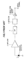
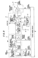
- Fig. 1 shows a conventional infrared ray receiving circuit.
- the conventional infrared ray receiving circuit includes an infrared ray detector 1, an amplifier 2, a BPF 3, a detector 4, and a wave-form shaping circuit 5.
- a PPM signal consisting of a carrier wave of a specific wavelength having ON and OFF durations is transmitted from a transmitting apparatus to an infrared ray receiving circuit and received by the infrared ray detector 1.
- the infrared detector 1 detects the PPM signal to be supplied to the amplifier 2.
- the amplifier 2 amplifies the PPM signal with an adequate gain to supply the amplified PPM signal to the BPF 3.
- the BPF 3 which is tuned with the carrier wave of the PPM signal removes unnecessary signals or noises from the PPM signal to supply the tuned PPM signal to the detector 4.
- the detector 4 detects the PPM signal having low and high durations to be supplied to the wave-form shaping circuit 5.
- the wave-form shaping circuit 5 generates a pulse signal determined by the low and high durations of the PPM signal supplied from the detector 4, and supplies the pulse signal to an output terminal 6 connected to a device such as a microcomputer, etc.
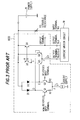
- Fig. 2 shows detailed circuitry structures of the BPF 3, the detector 4 and the wave-form shaping circuit 5 in the infrared ray receiving circuit.
- the BPF 3 includes first and second variable trans-conductance amplifiers 11 and 13, first and second buffers 12 and 14.
- the first variable trans-conductance amplifier 11 is connected at a non-reversed input terminal to a positive terminal of a power supply 113, at a reversed input terminal to an output terminal of the second buffer 14, at an output terminal to a nodal point A, and at a positive control terminal to an output 19.2 of a first current mirror circuit 19.
- the first buffer 12 is connected at an input terminal to the nodal point A and at an output terminal to a non-reversed input terminal of the second variable trans-conductance amplifier 13.
- the second variable trans-conductance amplifier 13 is connected at a reversed input terminal to an output terminal of the second buffer 14, at an output terminal to a nodal point B, and at a positive control terminal to an output terminal 19.4 of the first current mirror circuit 19.
- the second buffer 14 is connected at an input terminal to the nodal point B and at on output terminal to an input of the detector 4.
- An input terminal of the BPF 3 which is connected to the amplifier 2 is connected to the nodal point A through a first capacitance C1.
- the nodal point B is connected to ground through a second capacitance C2.
- the first current mirror circuit 19 is connected at an input terminal 19.1 to a positive terminal of a power supply 111 through a variable resistance R3.
- the detector 4 includes a DC level shift circuit 15, a low pass filter 16, first and second NPN transistors Q100 and Q101 together composing a differential switch, and a current mirror circuit 17.
- the DC level shift circuit 15 is connected at an input terminal to an output of the BPF 3 and a base of the second NPN transistor Q101, and an output terminal to an input terminal of the low pass filter 16.
- the low pass filter 16 is connected at an output terminal to a base of the first NPN transistor Q100.
- the first NPN transistor Q100 is connected at an emitter to an output terminal 23.2 of the second current mirror circuit 23.
- the second NPN transistor Q101 is connected at an emitter to the output terminal 23.2 of the second current mirror circuit 23 and at a collector to an output terminal 17.1 of the current mirror circuit 17.
- An output 17.2 of the current mirror circuit 17 is connected to a nodal point C.
- the nodal point C is connected to an input of the wave-form shaping circuit 5, an output terminal 23.3 of the second current mirror circuit 23, and ground through a capacitance C3.
- An output terminal 23.1 of the second current mirror circuit 23 is connected to a positive terminal of the power supply 111 through a resistance R4.
- the wave-form shaping circuit 5 includes a hysteresis comparator 18.
- the hysteresis comparator 18 is connected at an input terminal to the nodal point C of the detector 4, at an output terminal to an output terminal 6 of the infrared ray receiving circuit, and at a hysteresis width control terminal to an output terminal 20.2 of the third current mirror circuit 20.
- An input 20.1 of the third current mirror circuit 20 is connected to a positive terminal of the power supply 111 through a resistance R11.
- Fig. 3 shows an example of a circuitry structure of the first and second variable trans-conductance amplifiers 11 and 13.
- the variable trans-conductance amplifier includes first to fourth NPN transistors Q1 to Q4, first and second PNP transistors Q5 and Q6, first and second diodes D1 and D2, first and second resistances R1 and R2, and a current supply 11.
- the first NPN transistor Q1 is connected at a base to the non-reversed input terminal of the variable trans-conductance amplifier, at a collector to a nodal point D, and an emitter to one terminal of the first resistance R1.
- the second NPN transistor Q2 is connected at a base to the reversed input terminal thereof, at a collector to a nodal point E, and at an emitter to one terminal of the second resistance R2.
- the first and second resistances R1 and R2 are connected in common to a nodal point F.
- the current supply 11 is connected between the nodal point F and ground.
- the first diode D1 is connected at a cathode to the nodal point D and at an anode to a positive terminal of the power supply 111.
- the second diode D2 is connected at a cathode to the nodal point E and at an anode to the positive terminal of the power supply 111.
- the third NPN transistor Q3 is connected at a base to the nodal point E, at a collector to a nodal point G, and at an emitter to a nodal point J which is connected to an output 19.2 (19.4) of the first current mirror circuit 19.
- the fourth NPN transistor Q4 is connected at a base to the nodal point D, at a collector to the positive terminal of the power supply 111, and at an emitter to the nodal point J.
- the first PNP transistor Q5 is connected at a base to a nodal point H which is connected to the nodal point G, at a collector to the nodal point G, and at an emitter to the positive terminal of the power supply 111.
- the second PNP transistor Q6 is connected at a base to the nodal point H, at a collector to an output terminal of the variable trans-conductance amplifier 11(13), and at an emitter to the positive terminal of the power supply 111.
- the mutual conductance g m becomes large as I 2 becomes large, and becomes small as I 1 becomes large.
- a terminal connected to the nodal point F through which the pulling current I 1 flows will be called as a negative control terminal
- a terminal connected to the nodal point J through which the pulling current I 2 flows will be called as a positive control terminal.
- the mutual conductance g m is adjusted by varying the value of I 2 while I 1 is fixed to be a predetermined value.
- f 0 can be adjusted by varying I 1 with using the variable resistance R3.
- the tuning frequency f 0 may be affected by dispersions of values of the resistances and capacitances due to the change of conditions of the impurity diffusion steps in the fabrication process thereof, because the infrared ray receiving circuit is fabricated in the semiconductor process. If the values of the resistances change, the currents also change. As understood by the formula (2), I 1 may not affect the value of f 0 substantially as it is multiplied with R E , however, I 2 may affect the value of f 0 . Therefore, the variable resistance R3 is provided separately outside the integrated circuit mainly composing the infrared ray receiving circuit to avoid dispersion of the value of the resistance R3 due to the dispersion of the process conditions.
- C 1 and C 2 may also affect the value of f 0 . Therefore, the value of the variable resistance R3 is adjusted after the fabrication of the integrated circuit composing the infrared ray receiving circuit to cancel the change of C 1 and C 2 .
- Fig. 4A shows an example of the PPM signal supplied to the infrared ray receiving circuit.
- the PPM signal includes ON duration of the carrier wave and OFF duration of only a DC level signal.
- the PPM signal is divided to be transmitted through two electrical paths, one of which is supplied directly to the base of the NPN transistor Q101, and the other is supplied to the DC level shifting circuit 15 where its DC level is increased to be a predetermined level.
- the DC level shifted signal is supplied to the low pass filter 16 where the component of the carrier wave is stopped, and then is supplied to the base of the NPN transistor Q100.
- the signal supplied to the base of the NPN transistor Q100 is used as a reference signal of a threshold for the PPM signal supplied to the base of the NPN transistor Q101.
- Fig. 4B shows the signals supplied to the bases of the NPN transistors Q100 and Q101.
- the NPN transistor Q101 becomes at ON state when the base potential of the NPN transistor Q101 is higher than that of the NPN transistor Q100, and a collector current thereof begins flowing through the current mirror circuit 17 having input/output current ratio of 1:1 from the output terminal thereof.
- the capacitance C3 is charged by a difference current of I 4 and I 3 when the NPN transistor Q101 is at ON state and is discharged to make flow the current I 3 when the NPN transistor Q101 is at OFF state.
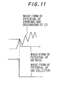
- Fig. 4C shows the charging and discharging potentials of the capacitance C3.
- the potential of the capacitance C3 increases to be a high level with having a saw-tooth wave due to the charging by the difference between I 4 and I 3 and the discharging by only I 3 at the ON duration of the PPM signal, and decreases to be a low level by discharging of I 3 at the OFF duration thereof.
- the signal of saw-tooth wave supplied from the capacitance C3 is restored to be square waves obtained at the output terminal 6.
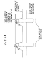
- Fig. 5 shows an example of the hysteresis comparator 18 composing the wave-form shaping circuit 5.
- the hysteresis comparator 18 includes three NPN transistors Q11, Q12 and Q15, two PNP transistors Q13 and Q14, and three resistances R11 to R13.
- the NPN transistor Q11 is connected at a base to an input terminal to which the signal of saw-tooth wave is supplied, at a collector to a nodal point K which is connected to the output terminal 6, and at an emitter to a nodal point 0.
- the NPN transistor Q12 is connected at a base to a nodal point N, at a collector to a nodal point L, and at an emitter to the nodal point 0.
- the NPN transistor Q15 is connected at a base to a positive terminal of a power supply 112, at a collector to a positive terminal of the power supply 111, and at an emitter to a nodal point P which is connected to an output terminal 20.3 of the current mirror circuit 20.
- the PNP transistor Q13 is connected at a base to a nodal point M which is connected to the nodal point L, at a collector to the nodal point L, and at an emitter to the positive terminal of the power supply 111.
- the PNP transistor Q14 is connected at a base to the nodal point M, at a collector to the nodal point N, and at an emitter to the positive terminal of the power supply 111.
- the resistance R11 is connected between the positive terminal of the power supply 111 and an input terminal 20.1 of the current mirror circuit 20.
- the resistance R12 is connected between the nodal points N and P.
- the resistance R13 is connected between the positive terminal of the power supply 111 and the nodal point K.
- Fig. 6A shows the base potentials of the NPN transistors Q11 and Q12
- Fig. 6B shows the potential of the output terminal 6.
- a collector current of the NPN transistor Q12 flows through the resistance R12 from a current mirror circuit consisting of the PNP transistors Q13 and Q14, so that the base potential of the NPN transistor Q12 increases to be high.
- the voltage generated across the two terminals of the resistance R12 is represented by the following formula (5): I 5 ⁇ R 12 where I 5 is the pulling current of the output terminal 20.2 of the current mirror circuit 20 and R 12 is the value of the resistance R12. Therefore, a differential amplifier consisting of the NPN transistors Q11 and Q12 can operate as a hysteresis comparator having a threshold voltage of I 5 ⁇ R 12 . The threshold voltage thereof is proportional to I 5 , so that it can be controlled by changing the value of I 5 .
- the PPM modulated signal is removed of unnecessary signal components and noises, detected and shaped by the BPF 3, the detector 4 and the wave-form shaping circuit 5 to be obtained at the output terminal 6.
- the charging and discharging potentials of C3 are represented by the formulas (3) and (4), however, the potential thereof changes in accordance with the change of the value of the capacitance C3, the pulling current I 3 of the output terminal 23.3 of the current mirror circuit 23, the collector current I 4 of the NPN transistor Q101 at ON state, and the frequency f 1 of the carrier wave of the PPM signal.
- the values of the capacitances and the resistances in the infrared ray receiving circuit vary due to the dispersion of the conditions of the fabrication process thereof.
- the difference between the charging and discharging potentials of C3 (the difference between a peak and a bottom of a voltage of C3) becomes greater than a hysteresis width as originally prescribed, so that hair peaks are generated in the output signal of the hysteresis comparator 18, as shown in Fig. 7.
- the potential of C3 may not increase to be high sufficiently at a state that a PPM signal having a short ON duration is supplied thereto, so that the pulse width of the output signal of the hysteresis comparator 18 becomes short, as shown in Fig. 8C.
- the output signal of the hysteresis comparator 18 is supplied directly to the output terminal 6 as an output signal of the infrared ray receiving circuit, so that the generation of the output signal having the hair peaks or the short pulse width causes malfunction of a device such as a microcomputer, etc. connected with the output terminal 6.
- the basic structure of the infrared ray receiving circuit is the same as that of the conventional infrared ray receiving circuit in Fig. 1, except that a hysteresis comparator 18 composing an wave-form shaping circuit 5 is supplied with a pulling current I 5 from an output terminal 19.5 of a current mirror circuit 19 which also supplies pulling currents to variable trans-conductance amplifiers of a BPF 3, the DC level shifting circuit 15 and the low pass filter 16 are connected between the input terminal and the base of the NPN transistor Q101 in the detector 4, and the variable trans-conductance amplifiers 11 and 13 are modified.
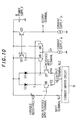
- Fig. 10 shows an example of a modified circuitry structure of the first and second variable trans-conductance amplifiers 11 and 13.
- the variable trans-conductance amplifier includes first to fourth NPN transistors Q16 to Q19, first and second PNP transistors Q20 and Q21, first and second diodes D3 and D4, first and second resistances R13 and R14, and first and second current supplies 12 and 13.
- the first NPN transistor Q16 is connected at a base to the non-reversed input terminal of the variable trans-conductance amplifier, at a collector to a nodal point S, and an emitter to one terminal of the first resistance R13.
- the second NPN transistor Q17 is connected at the reversed input terminal thereof, at a collector to a nodal point T, and at an emitter to one terminal of the second resistance R14.
- the first and second resistances R13 and R14 are connected in common to an output terminal 19.2 of the current mirror circuit 19.
- the first diode D3 is connected at a cathode to the nodal point S and at an anode to a positive terminal of the power supply 111.
- the second diode D4 is connected at a cathode to the nodal point T and at an anode to the positive terminal of the power supply 111.
- the third NPN transistor Q18 is connected at a base to the nodal point T, at a collector to a nodal point U, and at an emitter to a nodal point Y.
- the fourth NPN transistor Q19 is connected at a base to the nodal point S, at a collector to the positive terminal of the power supply 111, and at an emitter to the nodal point Y.
- the first PNP transistor Q20 is connected at a base to a nodal point X which is connected to the nodal point U, at a collector to the nodal point U, and at an emitter to the positive terminal of the power supply 111.
- the second PNP transistor Q21 is connected at a base to the nodal point X, at a collector to an output terminal of the variable trans-conductance amplifier, and at an emitter to the positive terminal of the power supply 111.
- the first current supply I2 is connected between the nodal point Y and ground.
- the second current supply I3 is connected between the output terminal of the variable trans-conductance amplifier and ground.
- variable trans-conductance amplifier can be changed in accordance with the change of the pulling current I 1 of the output terminal 19.2 of the current mirror circuit 19 by changing the value of the variable resistance R3 while fixing the current I 2 of the current supply I2.
- the values of the capacitances C1 and C2 of the BPF 3 become also small in proportion to that of the capacitance C3, because the capacitances C1 to C3 are fabricated to be matched each other in the same process, so that the tuning frequency f 0 becomes large, as understood by the formula (2).
- the tuning frequency f 0 becomes small.
- the hysteresis width of the hysteresis comparator 18 can be adjusted by adjusting f 0 by changing the value of the variable resistance R3 to be small or large to make I 1 large or small and changing the pulling current I 5 of the output terminal 19.5 of the current mirror circuit 19 to be large or small.
- the hysteresis width of the hysteresis comparator 18 can be adjusted by adjusting f 0 by changing the value of the variable resistance R3 to be small or large to make I 1 large or small and changing the pulling currentI 5 of the output terminal 19.5 of the current mirror circuit 19 to be large or small.
- the hysteresis width of the hysteresis comparator 18 can be adjusted by adjusting f 0 by changing the value of the variable resistance R3 to be small or large to make I 1 large or small and changing the pulling current I 5 of the output terminal 19.5 of the current mirror circuit 19 to be large or small.
- the hysteresis width of the hysteresis comparator 18 can be adjusted, so that the generation of hair peaks in the output signal of the hysteresis comparator 18 caused by the potential difference between the peak of the charging voltage of C3 and the bottom of the discharging voltage which is larger than the hysteresis width can be avoided.
- the wave-form of the output signal of the hysteresis comparator 18 is shown as that of the potential of the base of the NPN transistor Q12, and it is observed that there is no hair peak in the output signal thereof.
- the potential of C3 does not increase to be high sufficiently at a state that the PPM signal having short ON duration is supplied thereto, when a large capacitance is provided to avoid the generation of the hair peaks so that the pulse width of the output signal of the hysteresis comparator 18 becomes short.
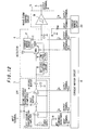
- the basic structure of the infrared ray receiving circuit is the same as that of the infrared ray receiving circuit in the first preferred embodiment, except that a hysteresis comparator 18 composing an wave-form shaping circuit 5 is supplied with a pulling current I 5 from a current mirror circuit 20, and a detector 4 is supplied with a pulling current from a current mirror circuit 19 which also supplies pulling currents to variable trans-conductance amplifiers of a BPF 3.
- an output terminal 19.6 of the current mirror circuit 19 which functions as a first constant current supply is connected in common to emitters of the NPN transistors Q100 and Q101 which compose a differential switch.
- the NPN transistor Q101 is connected at a collector to an input terminal 17.1 of a current mirror circuit 17.
- An output terminal 17.2 of the current mirror circuit 17 is connected to one terminal of a capacitance C3, an input terminal of a hysteresis comparator 18, and an output terminal 19.7 of the current mirror circuit 19.
- a current supplied from the output terminal 19.6 of the current mirror circuit 19 is reversed of polarization at the current mirror circuit 17, and is supplied to the capacitance C3 to be charged.
- An output terminal 19.7 of the current mirror circuit 19 as a second constant current supply functions as a current supply of discharging of the capacitance C3.
- Output terminals 19.2 and 19.4 of the current mirror circuit 19 functions as current supplies for determining the tuned frequency f 0 of the BPF 3.
- An input terminal 19.1 of the current mirror circuit 19 is connected to a power supply 111 through a variable resistance R3.
- the currents of the first and second current supplies are required to be small in order to obtain a predetermined wave-form of an input signal supplied to the hysteresis comparator 18.
- the values of the capacitances C1 and C2 of the BPF 3 become also small in proportion to that of the capacitance C3, because the capacitances C1 to C3 are fabricated to be matched each other in the same process, so that the value of the tuning frequency f 0 shifts to be large, as understood by the formula (2).
- the tuning frequency f 0 shifts to be small.
- the tuning frequency f 0 can be adjusted by changing the value of the variable resistance R3.
- the currents of the first and second constant current supplies can be also adjusted to be large or small by changing the value of the variable resistance R3. Therefore, the wave-form of the input signal of the hysteresis comparator 18 can be adjusted by adjusting the tuned frequency f 0 of the BPF 3 with using currents which are adjustable by the variable resistance R3 for the first and second constant current supplies of the BPF 3.
- the currents of the first and second constant current supplies are required to be small to adjust the wave-form of the input signal of the hysteresis comparator 18.
- the currents of the first and second constant current supplies are adjusted by changing the value of the variable resistance R3 to be large in conjunction with the matching operation of the frequency f 0 to the frequency of the carrier wave of the PPM signal.
- the wave-form of the input signal of the hysteresis comparator 18 can be maintained to be a predetermined wave-form.
- variable resistance R3 which may be replaced by a trimming resistance in some cases is provided separately with a semiconductor integrated circuit composing the infrared ray receiving circuit, and the wave-form of the input signal of the hysteresis comparator 18 is adjusted by the variable resistance R3, so that the wave-form thereof may not be affected by dispersion of the values of the resistances in the semiconductor integrated circuit.
Landscapes
- Physics & Mathematics (AREA)
- Electromagnetism (AREA)
- Engineering & Computer Science (AREA)
- Computer Networks & Wireless Communication (AREA)
- Signal Processing (AREA)
- Networks Using Active Elements (AREA)
- Optical Communication System (AREA)
- Amplifiers (AREA)
Claims (5)
- Circuit récepteur de rayons infrarouges, comprenant :caractérisé parun filtre passe-bande (3) comprenant des premier (11) et second (13) amplificateurs à transconductance variable, ledit filtre passe-bande (3) recevant un signal d'entrée à modulation PPM ;un détecteur (4) comprenant un commutateur différentiel, ledit détecteur recevant un signal de sortie dudit filtre passe-bande (3) ; etun circuit de mise en forme (5) comprenant un comparateur d'hystérésis (18), ledit circuit de mise en forme recevant un signal de sortie dudit détecteur ;le fait que lesdits premier (11) et second (13) amplificateurs à transconductance variable dudit filtre passe-bande (3) sont commandés par des premier et second signaux de sortie de première et seconde bornes de sortie d'un circuit formant miroir de courant (19) ; etle fait que ledit comparateur d'hystérésis (18) dudit circuit de mise en forme (5) est commandé par un troisième signal de sortie d'une troisième borne de sortie dudit circuit formant miroir de courant (19), de sorte qu'une largeur d'hystérésis dudit comparateur d'hystérésis (18) est ajustée par ledit troisième signal de sortie dudit circuit formant miroir de courant (19).
- Circuit récepteur de rayons infrarouges selon la revendication 1, dans lequel :ledit circuit formant miroir de courant (19) est muni d'une borne d'entrée connectée par l'intermédiaire d'une résistance variable (R3) à une alimentation électrique (111), lesdits premier à troisième signaux de sortie dudit circuit formant miroir de courant (19) ayant une valeur de courant ajustée par ladite résistance variable (R3).
- Circuit récepteur de rayons infrarouges selon la revendication 1, dans lequel chacun desdits premier (11) et second (13) amplificateurs à transconductance variable dudit filtre passe-bande comprend :des premier à quatrième transistors NPN (Q16, Q17, Q18, Q19), des premier et second transistors PNP (Q20, Q21), des première et seconde diodes (D3, D4), des première et seconde résistances (R13, R14), et des première et seconde alimentations en courant ; dans lequelledit premier transistor NPN (Q16) est connecté par une base à une borne d'entrée non inversée, par un collecteur, à un premier point nodal (S), et par un émetteur, à une première borne de ladite première résistance (R13) ;ledit second transistor NPN (Q17) est connecté par une base à une borne d'entrée inversée, par un collecteur, à un second point nodal (T), et par un émetteur, à une première borne de ladite seconde résistance (R14) ;ledit troisième transistor NPN (Q18) est connecté par une base audit second point nodal (T), par un collecteur, à un troisième point nodal (U), et par un émetteur, à un quatrième point nodal (Y) ;ledit quatrième transistor NPN (Q19) est connecté par une base audit premier point nodal (S), par un collecteur, à une borne positive d'une alimentation électrique (111), et par un émetteur, audit quatrième point nodal (Y) ;ledit premier transistor PNP (Q20) est connecté par une base à un cinquième point nodal (X) qui est connecté audit troisième point nodal (U), par un collecteur, audit troisième point nodal (U), et par un émetteur, à ladite borne positive de ladite alimentation électrique (111) ;ledit second transistor PNP (Q21) est connecté par une base audit cinquième point nodal (X), par un collecteur, à une borne de sortie dudit amplificateur à transconductance variable, et par un émetteur, à ladite borne positive de ladite alimentation électrique (111) ;lesdites première et seconde résistances (R13, R14) sont connectées en commun à chaque seconde borne de l'une ou l'autre desdites première et seconde bornes de sortie dudit circuit formant miroir de courant (19) ;ladite première diode (D3) est connectée par une cathode audit premier point nodal (S) et par une anode à ladite borne positive de ladite alimentation électrique (111) ;ladite seconde diode (D2) est connectée par une cathode audit second point nodal (T) et par une anode à ladite borne positive de ladite alimentation électrique (111) ;ladite première alimentation en courant est connectée entre ledit quatrième point nodal (Y) et la masse ; etladite seconde alimentation en courant est connectée entre ladite borne de sortie dudit amplificateur à transconductance variable et la masse.
- Circuit récepteur de rayons infrarouges comprenant :caractérisé parun filtre passe-bande (3) comprenant des premier (11) et second (13) amplificateurs à transconductance variable, ledit filtre passe-bande recevant un signal d'entrée à modulation PPM ;un détecteur (4) comprenant un commutateur différentiel, ledit détecteur recevant un signal de sortie dudit filtre passe-bande (3) ; etun circuit de mise en forme (5) comprenant un comparateur d'hystérésis (18), ledit circuit de mise en forme recevant un signal de sortie dudit détecteur (4) ;le fait que lesdits premier (11) et second (13) amplificateurs à conductance variable dudit filtre passe-bande (3) sont commandés par des premier et second signaux de sortie de première et seconde bornes de sortie d'un circuit formant miroir de courant (19) ; etle fait que ledit détecteur (4) est commandé par un troisième signal de sortie d'une troisième borne de sortie dudit circuit formant miroir de courant (19), de sorte qu'un niveau d'un signal de sortie dudit détecteur (4) est ajusté par ledit troisième signal de sortie dudit circuit formant miroir de courant (19).
- Circuit récepteur de rayons infrarouges selon la revendication 4, dans lequel :ledit circuit formant miroir de courant (19) est muni d'une borne d'entrée connectée par l'intermédiaire d'une résistance variable (R3) à une alimentation électrique (111), lesdits premier à troisième signaux de sortie dudit circuit formant miroir de courant ayant une valeur de courant ajustée par ladite résistance variable (R3).
Applications Claiming Priority (2)
| Application Number | Priority Date | Filing Date | Title |
|---|---|---|---|
| JP27174690 | 1990-10-09 | ||
| JP271746/90 | 1990-10-09 |
Publications (3)
| Publication Number | Publication Date |
|---|---|
| EP0480410A2 EP0480410A2 (fr) | 1992-04-15 |
| EP0480410A3 EP0480410A3 (fr) | 1994-01-26 |
| EP0480410B1 true EP0480410B1 (fr) | 1998-07-15 |
Family
ID=17504259
Family Applications (1)
| Application Number | Title | Priority Date | Filing Date |
|---|---|---|---|
| EP91117238A Expired - Lifetime EP0480410B1 (fr) | 1990-10-09 | 1991-10-09 | Circuit récepteur de rayons infrarouges |
Country Status (4)
| Country | Link |
|---|---|
| US (1) | US5216238A (fr) |
| EP (1) | EP0480410B1 (fr) |
| KR (1) | KR960014410B1 (fr) |
| DE (1) | DE69129780T2 (fr) |
Cited By (1)
| Publication number | Priority date | Publication date | Assignee | Title |
|---|---|---|---|---|
| DE102008058878A1 (de) * | 2008-11-26 | 2010-05-27 | Vishay Semiconductor Gmbh | Infrarot-Empfängerschaltung |
Families Citing this family (7)
| Publication number | Priority date | Publication date | Assignee | Title |
|---|---|---|---|---|
| US5432630A (en) * | 1992-09-11 | 1995-07-11 | Motorola, Inc. | Optical bus with optical transceiver modules and method of manufacture |
| US5508836A (en) * | 1994-09-13 | 1996-04-16 | Irvine Sensors Corporation | Infrared wireless communication between electronic system components |
| US5818328A (en) * | 1995-10-03 | 1998-10-06 | Audio Enhancement | Method and system for providing improved wireless audio transmission |
| AT410620B (de) | 1997-07-10 | 2003-06-25 | Efkon Entwicklung Forschung & Konstruktion Von Sondermaschinen Gmbh | Aufweckschaltung für ein elektronisches gerät |
| TW391084B (en) * | 1997-09-29 | 2000-05-21 | Sharp Kk | Data communication receiving element |
| JP2954127B2 (ja) * | 1998-01-30 | 1999-09-27 | 日本電気アイシーマイコンシステム株式会社 | 赤外線信号受信装置 |
| US6198766B1 (en) | 1998-03-17 | 2001-03-06 | International Business Machines Corporation | Method and apparatus for adaptive pre-demodulation pulse shaping |
Family Cites Families (8)
| Publication number | Priority date | Publication date | Assignee | Title |
|---|---|---|---|---|
| US4085411A (en) * | 1976-04-16 | 1978-04-18 | Sprague Electric Company | Light detector system with photo diode and current-mirror amplifier |
| US4072870A (en) * | 1976-06-30 | 1978-02-07 | Motorola, Inc. | Comparison circuit having programmable hysteresis |
| US4241455A (en) * | 1977-12-29 | 1980-12-23 | Sperry Corporation | Data receiving and processing circuit |
| DE2920208A1 (de) * | 1979-05-18 | 1980-11-27 | Oticon Electronics As | Empfaenger fuer moduliertes licht im sichtbaren und/oder infraroten bereich |
| DE2943867A1 (de) * | 1979-10-30 | 1981-05-07 | Siemens AG, 1000 Berlin und 8000 München | Fernsprechteilnehmerstation |
| GB2209105A (en) * | 1987-08-26 | 1989-04-26 | Philips Nv | Infra-red receiver |
| GB2222734A (en) * | 1988-09-12 | 1990-03-14 | Philips Electronic Associated | Optical radiation demodulator circuit |
| US5155353A (en) * | 1991-08-14 | 1992-10-13 | Tandberg Data | High dynamic range integrated opto-electronic sensor and MOSFET amplifiers for pulsed light |
-
1991
- 1991-10-09 US US07/774,719 patent/US5216238A/en not_active Expired - Lifetime
- 1991-10-09 DE DE69129780T patent/DE69129780T2/de not_active Expired - Lifetime
- 1991-10-09 KR KR1019910017662A patent/KR960014410B1/ko not_active IP Right Cessation
- 1991-10-09 EP EP91117238A patent/EP0480410B1/fr not_active Expired - Lifetime
Cited By (2)
| Publication number | Priority date | Publication date | Assignee | Title |
|---|---|---|---|---|
| DE102008058878A1 (de) * | 2008-11-26 | 2010-05-27 | Vishay Semiconductor Gmbh | Infrarot-Empfängerschaltung |
| US8744027B2 (en) | 2008-11-26 | 2014-06-03 | Vishay Semiconductor Gmbh | Infrared receiver circuit |
Also Published As
| Publication number | Publication date |
|---|---|
| EP0480410A2 (fr) | 1992-04-15 |
| KR960014410B1 (ko) | 1996-10-15 |
| KR920009110A (ko) | 1992-05-28 |
| DE69129780D1 (de) | 1998-08-20 |
| EP0480410A3 (fr) | 1994-01-26 |
| US5216238A (en) | 1993-06-01 |
| DE69129780T2 (de) | 1999-03-18 |
Similar Documents
| Publication | Publication Date | Title |
|---|---|---|
| US5430765A (en) | Digital data receiver having DC offset cancelling preamplifier and dual-mode transimpedance amplifier | |
| KR900002955B1 (ko) | 필터회로의 시정수 자동조정회로 | |
| US5844445A (en) | Feedback type pre-amplifier | |
| US6864751B1 (en) | Transimpedance amplifier with adjustable output amplitude and wide input dynamic-range | |
| US5291150A (en) | Control circuitry for an RF signal amplifier | |
| GB2107947A (en) | Improvements in or relating to transistor mixer and amplifier input stages for radio receivers | |
| US4492926A (en) | Amplitude modulation detector | |
| US4052679A (en) | Phase shifting circuit | |
| EP0480410B1 (fr) | Circuit récepteur de rayons infrarouges | |
| EP0862264A2 (fr) | Amplificateur à rétroaction et récepteur optique utilisant un tel amplificateur | |
| US6762596B2 (en) | Constant voltage circuit and infrared remote control receiver using the same | |
| EP0732807B1 (fr) | Dispositif de filtrage réglable | |
| CA1081791A (fr) | Recepteur am | |
| US5343170A (en) | Voltage controlled oscillator provided with negative feedback biasing | |
| US4642453A (en) | Apparatus for increasing the dynamic range in an integrating optoelectric receiver | |
| JPH03171908A (ja) | 光受信回路 | |
| JP3500960B2 (ja) | 光受信装置 | |
| JPH0282804A (ja) | 光受信用前置増幅器 | |
| US4904860A (en) | Optical signal detection circuit with constant current sources | |
| JPH08167819A (ja) | 送信回路 | |
| JPH04225611A (ja) | 広ダイナミックレンジ受光回路 | |
| US3579114A (en) | Automatic gain control system radio receivers and the like | |
| JP3322564B2 (ja) | 増幅回路 | |
| JP3088138B2 (ja) | 検波回路 | |
| JP3006319B2 (ja) | 受光回路 |
Legal Events
| Date | Code | Title | Description |
|---|---|---|---|
| PUAI | Public reference made under article 153(3) epc to a published international application that has entered the european phase |
Free format text: ORIGINAL CODE: 0009012 |
|
| AK | Designated contracting states |
Kind code of ref document: A2 Designated state(s): DE FR GB |
|
| 17P | Request for examination filed |
Effective date: 19920413 |
|
| PUAL | Search report despatched |
Free format text: ORIGINAL CODE: 0009013 |
|
| AK | Designated contracting states |
Kind code of ref document: A3 Designated state(s): DE FR GB |
|
| 17Q | First examination report despatched |
Effective date: 19961030 |
|
| GRAG | Despatch of communication of intention to grant |
Free format text: ORIGINAL CODE: EPIDOS AGRA |
|
| GRAG | Despatch of communication of intention to grant |
Free format text: ORIGINAL CODE: EPIDOS AGRA |
|
| GRAH | Despatch of communication of intention to grant a patent |
Free format text: ORIGINAL CODE: EPIDOS IGRA |
|
| GRAH | Despatch of communication of intention to grant a patent |
Free format text: ORIGINAL CODE: EPIDOS IGRA |
|
| GRAA | (expected) grant |
Free format text: ORIGINAL CODE: 0009210 |
|
| AK | Designated contracting states |
Kind code of ref document: B1 Designated state(s): DE FR GB |
|
| REF | Corresponds to: |
Ref document number: 69129780 Country of ref document: DE Date of ref document: 19980820 |
|
| ET | Fr: translation filed | ||
| PLBE | No opposition filed within time limit |
Free format text: ORIGINAL CODE: 0009261 |
|
| STAA | Information on the status of an ep patent application or granted ep patent |
Free format text: STATUS: NO OPPOSITION FILED WITHIN TIME LIMIT |
|
| 26N | No opposition filed | ||
| REG | Reference to a national code |
Ref country code: GB Ref legal event code: IF02 |
|
| REG | Reference to a national code |
Ref country code: GB Ref legal event code: 732E |
|
| REG | Reference to a national code |
Ref country code: FR Ref legal event code: TP |
|
| REG | Reference to a national code |
Ref country code: FR Ref legal event code: CD |
|
| PGFP | Annual fee paid to national office [announced via postgrant information from national office to epo] |
Ref country code: FR Payment date: 20101020 Year of fee payment: 20 |
|
| PGFP | Annual fee paid to national office [announced via postgrant information from national office to epo] |
Ref country code: DE Payment date: 20101006 Year of fee payment: 20 |
|
| PGFP | Annual fee paid to national office [announced via postgrant information from national office to epo] |
Ref country code: GB Payment date: 20101006 Year of fee payment: 20 |
|
| REG | Reference to a national code |
Ref country code: DE Ref legal event code: R071 Ref document number: 69129780 Country of ref document: DE |
|
| REG | Reference to a national code |
Ref country code: DE Ref legal event code: R071 Ref document number: 69129780 Country of ref document: DE |
|
| REG | Reference to a national code |
Ref country code: GB Ref legal event code: PE20 Expiry date: 20111008 |
|
| PG25 | Lapsed in a contracting state [announced via postgrant information from national office to epo] |
Ref country code: GB Free format text: LAPSE BECAUSE OF EXPIRATION OF PROTECTION Effective date: 20111008 |
|
| PG25 | Lapsed in a contracting state [announced via postgrant information from national office to epo] |
Ref country code: DE Free format text: LAPSE BECAUSE OF EXPIRATION OF PROTECTION Effective date: 20111010 |