EP0480331A2 - Système de traitement de données avec terminaux d'affichage - Google Patents
Système de traitement de données avec terminaux d'affichage Download PDFInfo
- Publication number
- EP0480331A2 EP0480331A2 EP91116966A EP91116966A EP0480331A2 EP 0480331 A2 EP0480331 A2 EP 0480331A2 EP 91116966 A EP91116966 A EP 91116966A EP 91116966 A EP91116966 A EP 91116966A EP 0480331 A2 EP0480331 A2 EP 0480331A2
- Authority
- EP
- European Patent Office
- Prior art keywords
- data processing
- processing system
- video
- address
- assigned
- Prior art date
- Legal status (The legal status is an assumption and is not a legal conclusion. Google has not performed a legal analysis and makes no representation as to the accuracy of the status listed.)
- Withdrawn
Links
Images

Classifications
-
- G—PHYSICS
- G06—COMPUTING; CALCULATING OR COUNTING
- G06F—ELECTRIC DIGITAL DATA PROCESSING
- G06F3/00—Input arrangements for transferring data to be processed into a form capable of being handled by the computer; Output arrangements for transferring data from processing unit to output unit, e.g. interface arrangements
- G06F3/14—Digital output to display device ; Cooperation and interconnection of the display device with other functional units
- G06F3/1423—Digital output to display device ; Cooperation and interconnection of the display device with other functional units controlling a plurality of local displays, e.g. CRT and flat panel display
- G06F3/1438—Digital output to display device ; Cooperation and interconnection of the display device with other functional units controlling a plurality of local displays, e.g. CRT and flat panel display using more than one graphics controller
Definitions
- the invention relates to a data processing system with a plurality of screen units.
- the system according to the invention is particularly intended for data processing devices such as personal computers, in which units which are usually controlled by a processor unit, for example a microprocessor, are controlled via a system bus, including a single display device, that is to say a monitor, which is connected to the system bus via a video adapter.
- a processor unit for example a microprocessor
- Various bus systems such as ISA, MCA or EISA and various standard video adapters such as VGA or EGA are used.
- the system bus is usually limited in terms of the transferable addresses, for example to 1 Mbyte, the first 640 Kbyte being reserved for data and further address areas for the BIOS system and other controls, so that the addresses available for a monitor are just for control purposes a single monitor is sufficient.
- the invention is therefore based on the object of specifying a data processing system with a plurality of screen units in which, despite the limited address capacity of the system bus of a data processing device, the control of a plurality of screen devices from one data processing device is made possible via standard video adapters. This can also be done in single-user mode.
- the control circuit according to the invention flexibly connects a plurality of display devices to the system bus via standard video adapters.
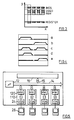
- FIG. 1 schematically shows the block diagram of a data processing system in which the control arrangement according to the invention is advantageously used.
- a microprocessor 12 and a system bus 14 are preferably mounted in a housing 10 on a main circuit board, through which the microprocessor 12 can communicate with the most varied units of the system.
- a peripheral unit 16 such as a hard disk shown, which is controlled via corresponding lines 15.
- a single monitor 26 is normally provided as a separate device, which is addressed from the system bus 14 via a standard video adapter 24, for example a VGA or EGA adapter, which is arranged on an expansion card in the housing 10.
- a standard video adapter 24 for example a VGA or EGA adapter, which is arranged on an expansion card in the housing 10.
- the system bus 14 has, for example, an address range of 1 Mbyte, of which only about 50 to 100 kByte are generally available for the video adapter 24, which are just sufficient for addressing and controlling it.
- the invention now creates the possibility of addressing a plurality of monitors via video adapters assigned to them by inserting at least one control circuit MVA 20, each MVA circuit producing the link between these video adapters and system bus 14.
- control circuits MVA 20 and 30 are shown, each of which address two video adapters 24, 25 or 36, 37 via VGA 24, 25 or VGA 34, 35.
- the number of MVA 20 and the number of video adapters 24, 25 they serve is not limited to two.
- eight video adapters can easily be operated from an MVA 20, which in turn establish the exchange of information with the system bus 14 via branched bus lines 17 and 18.
- FIG. 2 shows the MVA 20 in greater detail as an exemplary embodiment of the control circuit according to the invention.
- the branched bus 17 continues from the system bus 14 into the MVA 20 as the bus line 50 and branches into sub-bus lines 58 and 59, respectively, via the address, data and Control signals can be applied to the two VGA 24 and 25 via corresponding lines 22, 23.
- the circuit arrangement shown in FIG. 2 decides whether none or a specific one of the VGA 24 or 25 (and the associated monitor 26 or 27) is addressed.
- Each MVA 20 or 30 is assigned an I / O address of the system bus address area, which can also be set (primarily permanently) in a memory circuit 41, for example a register or the like.
- a comparison circuit 42 determines the occurrence of the I / O address stored in the memory circuit 41 via address lines 52 branched off from the system bus 50 and activates a selection register 44 into which a selection identifier is entered via lines 54.
- this selection identifier is a binary value 1-out-n, in the case of the exemplary embodiment therefore "01" or "10".
- the selection register 42 has a capacity of four bit positions to accommodate a 1-out-of-4 identifier, for example "0100”. If several MVA are operated, all but one, i.e. H. activated the identifier "0000".
- Each bit position corresponds to a different video adapter and is connected to an activation circuit 48 or 49 assigned to it via a line 45 or 56, in the simplest case this circuit 48, 49 can be a gate circuit whose output signal activates the assigned VGA 24 or 25 or deactivated in order to forward the information flow (addresses and data) pending on lines 58 and 59, respectively.
- the actual timing for this takes place via line 57, which leads from bus 50 to both circuits 48 and 49.
- the address windows for several video adapters are now addressed in an additional second dimension, the addressing in the second dimension being carried out by the control circuit MVA 20 or 30 according to the invention.
- FIG. 3 shows in the Y direction the usual division of the address space (first column) with addresses for registers which can be addressed via I / O signals.
- the address window for the video RAM of the VGA is located above or outside the actual data address space, and finally an address area for the BIOS is provided above it.
- the microprocessor 12 to a selected video adapter, e.g. B. VGA 24 transmitted image information is stored there and is continuously transmitted by this for image generation to the assigned monitor under refreshing, so that a still image is displayed. Meanwhile, the microprocessor 12 has enough Time to supply additional VGAs and monitors with appropriate register selection with image information via the same Y addresses.
- a selected video adapter e.g. B. VGA 24 transmitted image information is stored there and is continuously transmitted by this for image generation to the assigned monitor under refreshing, so that a still image is displayed.
- the microprocessor 12 has enough Time to supply additional VGAs and monitors with appropriate register selection with image information via the same Y addresses.
- each MVA 20, 30 is assigned an I / O register address.
- the comparison circuit 42 determines coincidence with the address stored in the memory circuit 41 and activates the register 44, into which the register content corresponding to the I / O register address is then transmitted via the lines 54 in the form of "01" or "10".
- a signal according to FIG. 4a is then applied to the control circuit 48 via line 45, while no signal occurs complementarily to this according to FIG.
- a 1-out-of-n decoder could be added to the register to activate the desired VGA.
- the registers 44 of all MVA are assigned the identifier "00".
- control circuits 48 and 49 can also be designed in such a way that, in order to deactivate the VGAs, the addresses supplied via the bus 50 are pushed out of the address window of the assigned adapter by addition.
- FIG. 5 shows an embodiment modified from FIGS. 1 and 2, in which each MVA 120 selects and controls exactly one VGA 24.
- the MVA 120 can advantageously be placed on the circuit board 110 of the video adapter VGA 24.
- the switching of the MVA 120 is then simplified since only an ON / OFF state has to be generated when the desired MVA 120 is activated.
Landscapes
- Engineering & Computer Science (AREA)
- Theoretical Computer Science (AREA)
- Computer Graphics (AREA)
- Human Computer Interaction (AREA)
- Physics & Mathematics (AREA)
- General Engineering & Computer Science (AREA)
- General Physics & Mathematics (AREA)
- Digital Computer Display Output (AREA)
- Bus Control (AREA)
- Controls And Circuits For Display Device (AREA)
Applications Claiming Priority (2)
| Application Number | Priority Date | Filing Date | Title |
|---|---|---|---|
| DE19904032044 DE4032044C2 (de) | 1990-10-09 | 1990-10-09 | Ansteuerschaltungsanordnung für ein Datenverarbeitungssystem mit mehreren Bildschirmeinheiten |
| DE4032044 | 1990-10-09 |
Publications (2)
| Publication Number | Publication Date |
|---|---|
| EP0480331A2 true EP0480331A2 (fr) | 1992-04-15 |
| EP0480331A3 EP0480331A3 (en) | 1992-09-16 |
Family
ID=6415949
Family Applications (1)
| Application Number | Title | Priority Date | Filing Date |
|---|---|---|---|
| EP19910116966 Withdrawn EP0480331A3 (en) | 1990-10-09 | 1991-10-04 | Data processing system with display terminals |
Country Status (3)
| Country | Link |
|---|---|
| EP (1) | EP0480331A3 (fr) |
| JP (1) | JPH04314095A (fr) |
| DE (2) | DE4032044C2 (fr) |
Cited By (4)
| Publication number | Priority date | Publication date | Assignee | Title |
|---|---|---|---|---|
| EP0579402A1 (fr) * | 1992-06-30 | 1994-01-19 | Loral Aerospace Corporation | Double carte de commande d'affichage pour Nubus |
| AU673542B2 (en) * | 1992-10-13 | 1996-11-14 | Sony Corporation | Method and apparatus for communicating between equipment units |
| WO1997014133A2 (fr) * | 1995-09-27 | 1997-04-17 | Cirrus Logic, Inc. | Circuits, systemes et procedes pour topographie memoire, et systems de commande d'affichage les utilisant |
| DE19603850A1 (de) * | 1996-02-05 | 1997-08-07 | Miro Computer Prod Ag | Grafikkarte zum Ansteuern zweier Bildschirme |
Citations (2)
| Publication number | Priority date | Publication date | Assignee | Title |
|---|---|---|---|---|
| US4884068A (en) * | 1986-09-12 | 1989-11-28 | Matheny Stephen E | Multiple display system |
| US4965559A (en) * | 1988-05-31 | 1990-10-23 | Motorola, Inc. | Multi-channel graphics controller |
Family Cites Families (3)
| Publication number | Priority date | Publication date | Assignee | Title |
|---|---|---|---|---|
| US4571671A (en) * | 1983-05-13 | 1986-02-18 | International Business Machines Corporation | Data processor having multiple-buffer adapter between a system channel and an input/output bus |
| US4642789A (en) * | 1983-09-27 | 1987-02-10 | Motorola Computer Systems, Inc. | Video memory controller |
| DD266196A1 (de) * | 1987-11-05 | 1989-03-22 | Militaerkartographischer Diens | Anordnung zur kopplung von digitalen bildspeichern an einen hostprozessor |
-
1990
- 1990-10-09 DE DE19904032044 patent/DE4032044C2/de not_active Expired - Fee Related
-
1991
- 1991-10-04 EP EP19910116966 patent/EP0480331A3/de not_active Withdrawn
- 1991-10-04 DE DE9115724U patent/DE9115724U1/de not_active Expired - Lifetime
- 1991-10-09 JP JP28941191A patent/JPH04314095A/ja active Pending
Patent Citations (2)
| Publication number | Priority date | Publication date | Assignee | Title |
|---|---|---|---|---|
| US4884068A (en) * | 1986-09-12 | 1989-11-28 | Matheny Stephen E | Multiple display system |
| US4965559A (en) * | 1988-05-31 | 1990-10-23 | Motorola, Inc. | Multi-channel graphics controller |
Non-Patent Citations (1)
| Title |
|---|
| IBM TECHNICAL DISCLOSURE BULLETIN. Bd. 32, Nr. 8A, Januar 1990, NEW YORK US Seiten 224 - 225; 'METHOD OF EXPANDING THE HARDWARE CAPABILITIES OF A PERSONAL COMPUTER SYSTEM WITH MINIMAL IMPACT TO SOFTWARE DRIVERS' * |
Cited By (6)
| Publication number | Priority date | Publication date | Assignee | Title |
|---|---|---|---|---|
| EP0579402A1 (fr) * | 1992-06-30 | 1994-01-19 | Loral Aerospace Corporation | Double carte de commande d'affichage pour Nubus |
| AU673542B2 (en) * | 1992-10-13 | 1996-11-14 | Sony Corporation | Method and apparatus for communicating between equipment units |
| WO1997014133A2 (fr) * | 1995-09-27 | 1997-04-17 | Cirrus Logic, Inc. | Circuits, systemes et procedes pour topographie memoire, et systems de commande d'affichage les utilisant |
| WO1997014133A3 (fr) * | 1995-09-27 | 1997-08-28 | Cirrus Logic Inc | Circuits, systemes et procedes pour topographie memoire, et systems de commande d'affichage les utilisant |
| US6025840A (en) * | 1995-09-27 | 2000-02-15 | Cirrus Logic, Inc. | Circuits, systems and methods for memory mapping and display control systems using the same |
| DE19603850A1 (de) * | 1996-02-05 | 1997-08-07 | Miro Computer Prod Ag | Grafikkarte zum Ansteuern zweier Bildschirme |
Also Published As
| Publication number | Publication date |
|---|---|
| JPH04314095A (ja) | 1992-11-05 |
| DE4032044C2 (de) | 1994-02-03 |
| DE9115724U1 (de) | 1992-04-09 |
| EP0480331A3 (en) | 1992-09-16 |
| DE4032044A1 (de) | 1992-04-16 |
Similar Documents
| Publication | Publication Date | Title |
|---|---|---|
| DE2753063C3 (fr) | ||
| DE3219379C2 (fr) | ||
| DE2536616C3 (de) | Schaltungsanordnung zur Verbindung einer eine Eingabetastatur und eine Anzeigeeinrichtung enthaltenden Engabe/Ausgabe-Einrichtung über eine Busleitung mit einem zu einem Mikrorechner gehörenden Mikroprozessor | |
| DE3854172T2 (de) | Verfahren und Vorrichtung zur Steuerung von zwei oder mehreren Bilddarstellungsgeräten. | |
| DE69123952T2 (de) | Rechneradressierungseinrichtung | |
| DE3318829C2 (de) | Ausgangsstufe einer Schnittstelle in einem Bussystem | |
| DE3015875A1 (de) | Speicherzugriffssystem und verfahren fuer einen zugriff zu einem digitalen speichersystem | |
| DE2926322C2 (de) | Speicher-Subsystem | |
| DE3022118A1 (de) | Treiber fuer zeichen/graphik-anzeigegeraet | |
| DE19614237C1 (de) | Kommunikationssystem mit einer Meisterstation und mindestens einer Sklavenstation | |
| DE2703559A1 (de) | Rechnersystem | |
| DE2758829A1 (de) | Multiprozessor-datenverarbeitungssystem | |
| DE3013064C2 (de) | Schaltungsanordnung zur Übertragung von Bitgruppen zwischen einer von mehreren peripheren Einheiten und einem Pufferspeicher | |
| DE4027205A1 (de) | Adressierungssystem fuer dynamisches ram | |
| DE19628039B4 (de) | Speicheradressen-Steuerschaltung | |
| DE2142374C2 (de) | Schaltungsanordnung zur Auswahl und ggfs. erfolgenden Modifizierung von Datenzeichen | |
| DE4032044C2 (de) | Ansteuerschaltungsanordnung für ein Datenverarbeitungssystem mit mehreren Bildschirmeinheiten | |
| DE69433033T2 (de) | Zeitverschachtelte leseschreiboperationen in einem hochgeschwindigkeitsrasterpuffersystem | |
| EP1145113B1 (fr) | Procede et dispositif permettant de produire et d'executer les programmes comprimes d'un processeur a tres long mot instruction | |
| DE2636788C3 (de) | Datenspeicher für Datensichtgeräte | |
| DE69425426T2 (de) | Mehrfache blockmodus-operationen in einem rasterpuffersystem für fensteroperationen | |
| EP0782077B1 (fr) | Procédé et arrangement pour convertir des adresses de mémoire en signaux de commande de mémoire | |
| DE4100018A1 (de) | Verfahren und anordnung zur bedienungsbedarfsmitteilung zwischen zwei stationen eines computerbusses | |
| DE2233164A1 (de) | Schaltungsanordnung zur ausblendung eines beliebig waehlbaren bereichs einer bitfolge bei deren uebertragung zwischen zwei registern | |
| EP0880092B1 (fr) | Dispositif à commande programmée avec possibilité de chargement et de mise en opération d'un deuxième système d'exploitation, sans interruption de l'exécution du dispositif |
Legal Events
| Date | Code | Title | Description |
|---|---|---|---|
| PUAI | Public reference made under article 153(3) epc to a published international application that has entered the european phase |
Free format text: ORIGINAL CODE: 0009012 |
|
| AK | Designated contracting states |
Kind code of ref document: A2 Designated state(s): AT CH DE FR GB LI NL |
|
| PUAL | Search report despatched |
Free format text: ORIGINAL CODE: 0009013 |
|
| AK | Designated contracting states |
Kind code of ref document: A3 Designated state(s): AT CH DE FR GB LI NL |
|
| STAA | Information on the status of an ep patent application or granted ep patent |
Free format text: STATUS: THE APPLICATION IS DEEMED TO BE WITHDRAWN |
|
| 18D | Application deemed to be withdrawn |
Effective date: 19930317 |