EP0479230A2 - Procédé de restauration et appareil pour une unité de traitement en pipeline d'un système à multiprocesseur - Google Patents
Procédé de restauration et appareil pour une unité de traitement en pipeline d'un système à multiprocesseur Download PDFInfo
- Publication number
- EP0479230A2 EP0479230A2 EP91116756A EP91116756A EP0479230A2 EP 0479230 A2 EP0479230 A2 EP 0479230A2 EP 91116756 A EP91116756 A EP 91116756A EP 91116756 A EP91116756 A EP 91116756A EP 0479230 A2 EP0479230 A2 EP 0479230A2
- Authority
- EP
- European Patent Office
- Prior art keywords
- uev
- unit
- bus
- stage
- stages
- Prior art date
- Legal status (The legal status is an assumption and is not a legal conclusion. Google has not performed a legal analysis and makes no representation as to the accuracy of the status listed.)
- Granted
Links
Images


Classifications
-
- G—PHYSICS
- G06—COMPUTING; CALCULATING OR COUNTING
- G06F—ELECTRIC DIGITAL DATA PROCESSING
- G06F11/00—Error detection; Error correction; Monitoring
- G06F11/07—Responding to the occurrence of a fault, e.g. fault tolerance
- G06F11/0703—Error or fault processing not based on redundancy, i.e. by taking additional measures to deal with the error or fault not making use of redundancy in operation, in hardware, or in data representation
- G06F11/0793—Remedial or corrective actions
-
- G—PHYSICS
- G06—COMPUTING; CALCULATING OR COUNTING
- G06F—ELECTRIC DIGITAL DATA PROCESSING
- G06F11/00—Error detection; Error correction; Monitoring
- G06F11/07—Responding to the occurrence of a fault, e.g. fault tolerance
- G06F11/0703—Error or fault processing not based on redundancy, i.e. by taking additional measures to deal with the error or fault not making use of redundancy in operation, in hardware, or in data representation
- G06F11/0706—Error or fault processing not based on redundancy, i.e. by taking additional measures to deal with the error or fault not making use of redundancy in operation, in hardware, or in data representation the processing taking place on a specific hardware platform or in a specific software environment
- G06F11/0721—Error or fault processing not based on redundancy, i.e. by taking additional measures to deal with the error or fault not making use of redundancy in operation, in hardware, or in data representation the processing taking place on a specific hardware platform or in a specific software environment within a central processing unit [CPU]
- G06F11/0724—Error or fault processing not based on redundancy, i.e. by taking additional measures to deal with the error or fault not making use of redundancy in operation, in hardware, or in data representation the processing taking place on a specific hardware platform or in a specific software environment within a central processing unit [CPU] in a multiprocessor or a multi-core unit
-
- G—PHYSICS
- G06—COMPUTING; CALCULATING OR COUNTING
- G06F—ELECTRIC DIGITAL DATA PROCESSING
- G06F11/00—Error detection; Error correction; Monitoring
- G06F11/07—Responding to the occurrence of a fault, e.g. fault tolerance
- G06F11/0703—Error or fault processing not based on redundancy, i.e. by taking additional measures to deal with the error or fault not making use of redundancy in operation, in hardware, or in data representation
- G06F11/0766—Error or fault reporting or storing
-
- G—PHYSICS
- G06—COMPUTING; CALCULATING OR COUNTING
- G06F—ELECTRIC DIGITAL DATA PROCESSING
- G06F11/00—Error detection; Error correction; Monitoring
- G06F11/004—Error avoidance
-
- G—PHYSICS
- G06—COMPUTING; CALCULATING OR COUNTING
- G06F—ELECTRIC DIGITAL DATA PROCESSING
- G06F11/00—Error detection; Error correction; Monitoring
- G06F11/22—Detection or location of defective computer hardware by testing during standby operation or during idle time, e.g. start-up testing
- G06F11/2205—Detection or location of defective computer hardware by testing during standby operation or during idle time, e.g. start-up testing using arrangements specific to the hardware being tested
Definitions
- the present invention relates to data processing systems and more particularly to fault tolerant systems.
- a fault tolerance strategy is considered to include one or more of the following elements. It includes masking (dynamic correction of generated errors); detection of errors (symptoms of faults); containment (prevention of error propagation across defined boundaries; diagnosis (identification of the faulty module responsible for a detected error; repair/reconfiguration (elimination or replacement of a faulty component or a mechanism for bypassing it); and system recovery (correction of the system to a state acceptable for continued operation.
- Recovery is defined as the continuation of system operation with data integrity after an error or fault occurs.
- Dynamic recovery has employed the use of self testing and dynamically checked logic circuits, most specifically in the form of interface error checkers.
- Implementation of dynamic hardware retry has been used to overcome the effects of transient hardware faults transparently to the rest of the system.
- RCU recovery control unit
- the RCU is used to analyze error signals, sometimes to perform rapid hardware diagnosis and sometimes to initiate interrupts for additional program aid such as diagnostics.
- the RCU provides the basis for dynamic interaction between hardware and software for recovery. This approach is described in greater detail in the article entitled "Logic Design for Dynamic Interactive Recovery” by W. C. Carter, et al., published in the November , 1971 issue of IEEE Transactions on Computers, Vol. C-20, No.11, pages 1300-1305.
- Faults are generally classified in terms of their duration, nature and extent.
- the duration of a fault can be transient, intermittent or permanent.
- a transient fault often, the result of external disturbances exists for a finite length of time and is non recurring.
- a system with an intermittent fault oscillates between faulty and fault-free operation which usually results from marginal or unstable (metastable) device operation.
- Permanent or so-called "hard” faults are device conditions that do not change or correct with time. They result from component failures, physical damage or design errors. It has been observed that intermittent faults (so-called soft faults) typically occur with greater frequency than "hard” faults. Such faults are more difficult to detect, since they may disappear after producing errors.
- the above and other objects of the present invention are achieved by the incorporation of the present invention method and apparatus into a production or pipelined central processing subsystem (CSS) unit such as the type of system which is subject of the related patent application of Ming-Tzer Miu and Thomas F. Joyce entitled, "Production Line Method and Apparatus for High Performance Instruction Execution.”
- the CSS unit is one processor of a closely coupled multiprocessor system in which the CSS unit connects in common to a system bus for sharing main memory and input/output resources such as peripheral, communications and input/output controllers/devices.
- Each CSS unit includes a plurality of VLSI chip circuit stages, some of which share common firmware controlled elements.
- the CSS unit includes a central processing unit (CPU), a virtual memory unit (VMU), and a cache unit.
- the cache unit connects to the system bus through a bus interface unit (BIU).
- the CPU includes an instruction unit stage (I Unit), an address unit stage (A Unit), and a number of parallel execution unit stages (E Unit, C Unit).
- the cache unit includes an instruction cache (I Cache) and a data cache (E Cache).
- the I Unit, A Unit and E Unit stages are constructed from custom VLSI chip circuits and occupy a first circuit board (mother board).
- the VMU, I Cache, and E Cache circuits occupy another circuit board (daughter board).
- the BIU interface circuits form part of the circuits of a second mother board.
- the BIU board also includes special registers and control circuits used to respond to certain types of unusual event (UEV) signals indicating that a fault was detected and for initiating certain actions to preserve the integrity of system data.
- UUV unusual event
- each circuit board includes one or more UEV detector circuits designed to detect when the pipeline stage associated therewith is exhibiting abnormal behavior.
- abnormal behavior refers to the performance of operations by a stage which do not make sense in terms of the functions normally performed by such stage.
- these detector circuits are capable of detecting abnormal behavior conditions such as an assumption of an unusual machine state which does not make sense in terms of the input signals being applied, the sending or receiving of an improper sequence of commands in which there is an attempt to perform an operations which is inconsistent with a previously performed operation or an attempt to access a firmware control store location which is inconsistent with normal operation.
- the UEV detector circuits provide an early opportunity for detecting behavioral symptoms indicative of when the CSS unit is acting abnormally or improperly. Since in such cases it becomes unwise to continue instruction execution, the CSS unit is caused to stop operating in a pipelined mode and is made to switch to a nonpipelined mode allowing the firmware controlled CPU to establish control of the CSS unit.
- an UEV fault signal is sent to the BIU control circuits.
- the BIU broadcasts the CSS UEV fault signal to all of the CSS stages. This broadcasted signal causes the pipelined stages to emulate completion of all of the instructions within the pipeline so as to flush it out.
- all memory write operations/commands are permitted to flow down to the point in the CSS unit where they are received by the BIU.
- the BIU In response to such requests, the BIU generates a ready signal to the requesting stage indicating that the operation was performed without actually writing the data into memory.
- the cache unit stage will convert all cache misses into hits enabling the stages to complete their outstanding operations with what is believed to be valid data.
- the firmware control store unit of the E Unit includes a UEV microcode firmware handler routine which is branched to by the E Unit. This routine writes into a group of A unit register file working register locations, the contents of the syndrome registers included within each circuit board. It writes into a last working location in the group indications for indicating whether or not it was an external or internal UEV and if internal, whether it was a firmware or hardware UEV. In the case of a firmware UEV, the firmware address which produced the UEV is also written into the working location.
- the firmware trap handler routine in response to the UEV condition, causes all of the syndrome register contents to be written into a specially allocated extension area of the normal trap save area which is the area normally reserved for storing context information. This enables the operating system to preserve the hardware and firmware behavioral information, in addition to other status information for further analysis.
- the syndrome registers include the UEV fault indicators in addition to key error conditions which further define the nature of the environment when the fault occurred.
- the UEV handler routine causes the clearing of a BIU UEV interrupt indicator enabling it to resume communications with the system bus.
- the UEV handler routine also causes a unique trap to be constructed which indicates if the detected fault was internal or external to the CSS unit. The generation of the trap is based upon an analysis of different bits within certain syndrome registers, in addition to other context information.
- the UEV handler routine In the absence of another UEV fault having occurred indicative of a "hard" fault condition, the UEV handler routine enables the I Unit to load its address counter to fetch the first instruction of the trap handler software and the pipeline is able to resume instruction execution.
- the extensive information provided concerning hardware and firmware behavior through the use of UEV detector circuits and error indicator information enable the operating system software to make its own determination as to whether or not it agrees with the hardware that the fault was "soft" or transient in nature and does not jeopardize the overall integrity of the system. That is, the operating system from its perspective is able to reliably determine if the system still is trustworthy.
- the victim task i.e., the task which was running during the occurrence of the UEV condition
- the victim task was a critical systems task or a user task running a critical system function such as where it was running and failed when it was manipulating a semaphore operation or holding a spin lock.
- the trap handler software determines that the integrity of the operating system is in doubt even though the underlying hardware and firmware had signalled that it is trustworthy, the software causes the system to switch to a high priority processing level.
- the operating system software Based upon whether the trap was external or internal, the operating system software captures different information which is forwarded to a technical assistance (service) center (TAC) where further analysis can be performed. Where the trap signaled an internal CSS fault, the operating system forwards syndrome register contents stored in the extended trap save area to the TAC where it is written into an error log. The operating system software will continue operating and will terminate the task which was running at the time of the internal trap condition.
- TAC technical assistance
- the invention's use of separate syndrome registers within each circuit board facilitates the TAC's identification of the optimum replaceable unit (ORU) or circuit board which produced the UEV fault.
- the methodology of the present invention makes it possible for the system to recover from transient or soft faults in a reliable fashion. It also provides for the detection of faults through the collection of unusual event signals from detector circuits distributed within the different circuit boards of the CSS unit which are sensitive to deviations in normal operational behavior by the pipelined stages.
- the UEV detector circuits within the BIU are able to detect abnormal behavior involving system bus operations or any other buses to which the CSS unit is required to connect.
- the UEV detector circuits within the CPU stages are provided for signaling abnormal behavior occurring within the firmware control elements.
- the special BIU registers of the preferred embodiment stores system bus address information pertaining to the last physical address presented to the system bus as well as the address pertaining to a last lock memory operation.
- the CSS unit is able to provide the necessary information needed for reliable recovery based upon independent decisions made by both the hardware and firmware and software.
- the recovery process takes advantage of the fact that most faults are transient in nature and therefore will not render the system untrustworthy.
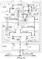
- FIG. 1 is a block diagram of a multiprocessor system which incorporates the method and apparatus of the present invention.
- FIG. 2a is a block diagram of the central subsystem (CSS) unit of Figure 1.
- FIG. 2b is a block diagram of the CSS unit showing in greater detail, the apparatus of the present invention.
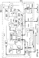
- FIGS 3a through 3f show in greater detail, the UEV detector circuits and BIU unit of Figure 2.
- Figures 4a through 4d illustrate in greater detail, the syndrome registers of Figure 2.
- Figures 5a through 5e are flow diagrams used in explaining the operation of the present invention.
- Figure 6 shows the organization of memory areas according to the present invention.
- FIG. 1 shows in block diagram form, a multiprocessor system 10 which incorporates the method and apparatus of the present invention.
- system 10 includes a system management facility (SMF) 12, a plurality of identical central subsystem (CSS) units 14-1 through 14-4, and a number of different subsystems 16 through 18 which are tightly coupled together by a system bus 11.
- the illustrative different subsystems include a number of memory subsystems 16-1 through 16-4 and a number of input/output subsystems 18-1 through 18-3.
- the CSS units 14-1 through 14-4 and memory subsystems 16-1 through 16-4 connect in common to a unidirectional asynchronous processor (P) bus 19.
- Each subsystem includes an interface unit which enables the subsystem to transmit or receive requests in the form of commands, interrupts, data or responses/status to another subsystem on the system bus 11 in an asynchronous manner.
- a termination network not shown defines the high priority end of bus 11.
- the SMF unit 12 which is positioned to the right of the termination network has the highest priority.
- Bus priority decreases as a function of each subsystem's distance from the termination network.
- the different subsystems communicate requests over system bus 11 on a priority basis defined by a distributed priority network included within system bus 11. For more detailed information regarding this arrangement, reference may be made to U.S. Patent No. 4,724,519.
- FIG. 2a shows in block diagram form, the central subsystem (CSS) unit 14 which takes the form of the production data processing system of the related patent application of Ming-Tzer Miu and Thomas F. Joyce.
- CSS unit 14 includes a central processing unit (CPU) 20, a virtual memory unit (VMU) 40 and a cache unit 60.
- the cache unit 60 couples to system bus 11 through a bus interface unit (BIU).
- BIU 100 has four interfaces. It serves as an interface for CPU 20, VMU and cache unit stages, system bus 11 and processor (P) bus 19.
- the main elements of CPU 20 include an instruction unit (I unit) stage 20-2, an address unit (A unit) stage 20-4 and an execution unit (E unit) stage 20-6.
- the execution unit stage 20-6 include a scientific unit (S-unit) and a commercial instruction processing unit (C-unit).
- the cache unit stage 60 includes an instruction cache (I-cache) 60-2 for storing instructions which are to be executed and an execution cache unit (E-cache) 60-4 for storing operands or data which are to be operated on according to the instructions being executed.
- the I-unit 20-2 performs two main functions. It prefetches instructions from the I-cache unit 60-2 and cracks or decodes these instructions to determine how the other units, namely the A-unit 20-4 and the E-unit 20-6 will further process those instructions. In addition, the I-unit 20-2 executes certain branch instructions which are then removed from the production line.
- the A-unit 20-4 generates addresses from instructions it receives from the I-unit 20-2. Additionally, it executes certain types of instructions such as register-to register type instructions removing them from the production line.
- the A-unit 20-4 sends a virtual address to VMU 40 which translates it into a physical address for fetching the specified operands from the E-cache unit 60-4.
- the operands fetched from the E-cache unit 60-4 are then transferred to the E-unit 20-6 for completing the execution of the instruction originally received by the I-unit 20-2 from the I-cache unit 60-2.
- the A-unit 20-4 will also confirm the execution of a branch instruction and send the branch address back to the I-unit 20-2 which will have already requested the next instruction from the I-cache unit 60-2 specified by the I-unit 20-2 prefetch branch address.
- both the A-unit 20-4 and E-unit 20-6 include register files which store the contents of the registers which are programmer accessible. Also, both the I-cache unit 60-2 and E-cache unit 60-4 are updated with instructions and operands fetched from main memory via system bus 11 and BIU 100.
- the I-unit stage 20-2 and A-unit stage 20-4 share a common firmware control store element 20-8.
- E-unit and C-unit execution units 20-6 share another common firmware control store element 20-10.
- VMU stage 40 and cache unit stage 60 occupy a daughter board which plugs into the CPU mother board.
- the system bus and P bus interface circuits of BIU 100 occupy another mother board.
- the entire CSS unit requires two socket card positions within the system.
- Instructions are executed in a production like fashion by the elements of CPU 20. That is, the I-unit 20-2 receives each instruction from I-cache stage 60-2, cracks it and then sends the instruction to the A-unit stage 20-4.
- the A-unit 20-4 either executes the instruction or sends the virtual address to VMU 40 for translation in order to fetch the required operands from E-cache stage 60-4 which are in turn sent to E-unit 20-6.
- the I-unit 20-2 While the A-unit 20-4 is executing its portion of a first instruction received from I-unit 20-2, the I-unit 20-2 is fetching a second instruction and subsequent instructions from I-cache stage 60-2. When the A-unit 20-4 sends the virtual address specified by the first instruction to VMU 40 and notifies the I-unit 20-2 of that event, the I-unit 20-2 sends the second instruction to A-unit 20-4.
- the VMU 40 addresses E-cache stage 60-4 while the A-unit 20-4 is processing the second instruction introduced into the production pipeline.
- VMU 40 may be fetching operands from the E-cache stage 60-4 specified by the second instruction while the A-unit 20-4 is generating a virtual address for a third instruction.
- the I-unit 20-2 is cracking a fourth instruction and fetching a next instruction. Thus, there could be five instructions progressing down the production line at a given instant of time.
- the I-unit 20-2 can execute certain branch instructions and the A-unit 20-4 can execute certain software visible register instructions, these instructions are removed from the production line as soon as the execution of these instructions are completed. Also, when the A-unit 20-4 is processing a branch instruction and the conditions of the branch are met, the A-unit 20-4 immediately confirms the branch address received from the I-unit 20-2 and the branch instruction is removed from the production line.
- Figure 2b shows the placement of different UEV detector circuits and syndrome registers within the APM, ACD, and ABM boards in accordance with the teachings of the present invention.
- Figure 2a also shows some of the different interface signals between the different pipelined stages used to synchronize operations therebetween.
- Each of the boards includes at least one syndrome register which is connected to receive signals from the UEV detector circuits within the different stages included on the board. Additionally, some of the syndrome registers are also connected to store error signal indications and other status information which are useful in carrying out fault analysis.
- the syndrome registers correspond to registers 20-12, 60-12 and 100-12 and 100-14.
- BIU 100 includes two syndrome registers, one for storing UEV indications and status information pertaining to the system bus 11 and another for storing UEV indications and status information pertaining to P bus 19. These signals are generated by the BIU bus interface circuits of block 100-20.
- the syndrome registers connect to data paths through which their contents can be transferred and written into working register locations included within the register file memories of CPU 20 as described herein. This occurs in response to control signals (i.e., readsyn) generated by the E-unit control store 20-10.
- the APM, ACD and ABM boards include programmable array logic (PAL) circuits 20-20, 60-20 and 100-24. Each PAL ORs together, the UEV fault signals stored in the syndrome register(s) associated therewith to produce the UEV fault output signals APMUEV, ACDUEV and BIUUEV. As shown, these signals are applied as inputs to the UEV collector and broadcast circuits of a block 100-16 included within BIU 100. These circuits collect and combine all of the UEV signals from the boards to produce a resulting UEV fault signal CSS UEV indicating when one of the stages has detected a UEV condition. As shown, this signal is broadcasted to the circuits included within each of the boards, causing the stages to take the required action for ensuring system data integrity and reliable recovery as explained herein.
- PAL programmable array logic
- interface request and ready signals which can be considered conventional for the purposes of the present invention.
- These signals include IREQT, DCN (I-unit/I-cache), AVCTL, VRDY (VMU/A-unit), ECRDY, VMUVAL (VMU/E-cache),and CAREQT, BIURDY (BIU/E-cache).
- FIGs 3a through 3g show in greater detail, the UEV detector and BIU100 circuits constructed according to the teachings of the present invention.
- Figure 3a shows in block diagram form, the UEV detector circuit included within VMU 40. This circuit is included as part of the state machine control of VMU 40.
- VMU 40 includes as part of its sequencing control, a state memory causes the generation of a VMU UEV signal when a bad state output signal is produced. This signal is generated when the specific combination of input signals forced the state memory to a location or state that does not make sense relative to the applied input signals.
- the VMU UEV signal indicates that the VMU 40 is misbehaving.
- FIG. 3b shows in block diagram form, the circuits included in the ABM board which detect circumstances when the E-cache stage 60-4 is misbehaving and generate UEV signals.
- these circuits include a programmable logic array circuit (PAL) 100-200 which receives a plurality of interface signals which correspond to commands being issued by the E-cache stage. Based upon the states of these signals, PAL 100-200 generates a UEV signal CMDUEV when it detects having received an illegal combination of commands which could not be successfully completed. That is, these commands, if executed, would result in extraordinary behavior. This results in setting a particular bit position (i.e., bit 23) in the P bus syndrome register 100-14.
- PAL programmable logic array circuit
- PAL 100-200 of Figure 3b receives command decode signals relating to illegal storage cycles being attempted by the E-cache stage. This involves the detection of when the cache stage is trying to execute a storage cycle and the write mask information furnished implies something which can not be translated onto the system bus in any meaningful way.
- the above store cycle cases include the situation where the write mask information implies that no bytes are to be written, or the write mask implies that non-consecutive bytes are to be written, or the write mask information implies non supported write operations (i.e. combinations of write commands that the memory will not execute).
- PAL 100-200 produces a UEV signal AUXUEV which results in the setting of another particular bit position (i.e., bit 22) within the P bus syndrome register 100-14 signaling a UEV fault condition.
- PAL 100-202 is used to detect unusual event lock request sequences which result in the setting of another particular bit position of syndrome register 100-12 (i.e. bit 14).
- PAL 100-202 operates to generate the lock signal LOCKUEV in response to either signal LOCKER+0A or signal LOCKER+0B.
- Signal LOCKER+0A is generated by PAL 100-200 when a lock clear command is specified to be done by the E-cache stage and the memory lock history indicator flip-flop is not active or on. It is also generated when a lock set command is specified to be done by the E-cache stage and the memory lock history indicator flip-flop is already active or on.
- the PAL 100-202 generates signal LOCKER+0B in response to auxiliary commands and checks for similar situations relative to the setting and clearing of the memory lock history indicator flip-flop. That is, it generates the LOCKUEV signal if the auxiliary command specifies a lock clear operation and the lock indicator flip-flop is already off or when the auxiliary command specifies a lock set operation and lock indicator flip-flop is already on.
- Figure 3d shows the circuits of block 100-204 for detecting failures inside and outside BIU 100. These include lack of synchronization, noise spikes, missing strobes or counter failures. These conditions if not detected can lead to cache incoherency problems.
- the P bus 19 is a 32 bit wide bus which provides a burst of 8 data words in response to a command issued via system bus 11 to main memory. When memory has the 8 words, it makes the P bus 19 busy and transfers the words in sequence.
- a PAL circuit 100-204 counts the data strobes and upon the receipt of the done signal verifies that the correct number of strobes have been received. If the count is other than that number, a UEV fault signal PBUSUEV is generated.
- Figure 3e shows in block diagram form, the types of firmware UEV fault detection that takes place in the control store 20-10. This enables the detection of lost interrupts, impossible branches or accessing unusual portions of the control store. When any one of these cases occur, the control store 20-10 is forced to a predetermined location which results in the generation of a UEV fault signal FWUEV.
- FWUEV UEV fault signal
- BIU 100 shows in block diagram form, the circuits of BIU 100 in greater detail. Some of these circuits have been already described.
- BIU 100 further includes a number of new registers. These include a lock address register 100-210, a physical address register 100-214 and a single bit power fail register 100-216.
- the lock address register 100-210 monitors the addresses being forwarded to the system bus 11 and saves the address associated with last lock operation performed by the CSS unit.
- the physical address register 100-214 is involved in the overall recovery process. If a failure occurs in the pipeline stages for any reason, the address contents of this register indicate to the software the last physical address or I/O channel number that was being used by the CSS unit in connection with accessing system bus 11.
- the power fail register 100-216 contains a bit position which is set to an active or binary ONE state to indicate the occurrence of a UEV fault. This is done when a power failure condition is detected and a time-out signal occurs indicating that the CSS unit has not responded to the power fail condition within a millisecond time interval.
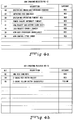
- Figures 4a through 4d show in greater detail the specific UEV and status information which is stored in the ABM, ACD, APM and P-BUS syndrome registers in accordance with the teachings of the present invention.
- the ABM syndrome register contains one or more different categories of signals. There are three different categories of signals and these are "red”, “yellow” and “no category”.
- the "red” designation indicates the occurrence of an uncorrectable error which include UEV faults.
- the "yellow” designation indicates the occurrence of an error which is not a UEV fault but which was correctable.
- the bits which have no category correspond to status information useful in fault isolation.
- bit 0 corresponding to signal CSSUAR designates an unavailable resource was attempted to be accessed by the CSS unit.
- Bit 2 indicates the state of all detected and collected RED indications.
- Bit 9 signals a red system bus time-out of 1/4 second.
- Bit 11 signals the occurrence of a power failure interrupt time-out.
- Bit 13 indicates when the memory lock was won by the CSS unit (signalled by an ACK).
- Bit 14 corresponding to signal LOCKUEV, indicates the occurrence of an UEV fault relating to inconsistent commands having been detected by the circuits of Figure 3c.
- Bit 29 is set when the CPU is unavailable denoted as APM busy.
- Bit 30 indicates when an error (parity) occurred in connection with the CPU control store on the APM board such as during the loading thereof or later during accessing.
- Figure 4b shows the allocation of bits within the ACD syndrome register.
- Bit 2 corresponding to signal VMUUEV indicates when the circuits of Figure 3a have detected that the VMU state machine has sequenced to an illogical state resulting in a UEV fault.
- Bits 4 and 5 designate the occurrence E-cache uncorrectable and correctable conditions based upon success of a retry operation.
- Figure 4c shows the allocation of bits within the APM syndrome register.
- Bit 12 corresponding to signal CSSUEV, indicates the occurrence of a UEV fault interrupt which is testable by the CSS unit firmware.
- Bits 14 through 17 indicate the detection of different stage parity errors.
- Bits 24 through 27 indicate occurrences of certain parity errors detected by checking circuits embedded within the different VLSI chips included within the I, A, C and E stages.
- Figure 4d shows the allocation of bits within the P-bus syndrome register.
- Bit 0 corresponding to PBUSUEV, indicates when the P-Bus circuits of Figure 3d detect an UEV fault condition.
- Bits 1 through 3 indicate the detection of uncorrectable bus parity error conditions.
- Bits 16 and 17 designate the CSS unit channel number (CSS0-3) while bits 18 and 19 indicate the occurrence of uncorrectable errors.
- the present invention enables the recovery of a CSS unit in a reliable fashion, thereby improving the fault tolerance and resiliency of a multiprocessor system, such as the system of Figure 1.
- it permits recovery only in those instances where the signalled fault is transient in nature or was due to operations external to the CSS unit.
- the flow chart of Figure 5a illustrates the overall process carried out by the apparatus and method of the present invention. It is a three phase process.
- the first phase is viewed as a hardware phase in which a hardware recovery procedure is initiated by the CSS unit.
- the second phase can be viewed as a firmware phase which is performed by CSS unit firmware and the third phase is viewed as a software phase which is carried by the operating system software.
- the CSS unit is operating normally until one of the UEV detector circuits detects that one of the stages on one of the three boards is misbehaving. Most of the time, this will be caused by an intermittent or transient condition.
- a UEV fault is detected by one of the UEV detector circuits, this causes a corresponding syndrome register bit position to be set.
- the syndrome register contents are monitored by one of the PAL circuits. When a change in state is detected, this causes the PAL to generate an output which results in one of the signals (APMUEV, ACDUEV or BIUUEV) being applied by one of the boards of Figure 2b as an input to the collector and broadcast circuits of block 100-16.
- the CSS UEV signal can be generated at any time during CSS unit operation, CPU 20 can have several instructions in process in the different pipelined stages.
- the CSS UEV signal allows the pipeline stages to be flushed. More specifically, the CSS UEV signal applied to the APM board causes the I-unit stage from starting any new instruction.
- the I-unit finishes the then current instruction with I-cache faked data, even without hits. That is, the CSS UEV signal applied to the ACD board causes the I-cache stage to emulate responding to I-unit requests for data. It will pretend to fake data when necessary in addition to converting misses to hits and allow the I-unit to finish the current instruction.
- the E-unit stage will also finish its current instructions of which there can be up to 4 instructions stored in the FIFO buffer which drives the pipeline inside the E-unit stage.
- the E-unit stage will receive faked data even without any hits. That is, signal CSS UEV causes the E-cache stage like the I-cache stage to furnish fake data when necessary in addition to converting misses to hits allowing the E-unit stage to finish executing its instructions.
- the BIU 100 in the presence of the CSS UEV signal emulates transfers of memory bus requests during the interval in which communications to the system bus 11 are stopped. For example, in the case of any memory write requests it receives from the ACD board, it will generate a BIURDY signal indicating that the operation was done without actually writing data into memory.
- the A and C unit stages do not respond to the UEV fault signal directly. That is, the I-unit stage is driven by the I firmware and in turn drives the I-cache stage.
- the E/C-unit stage is driven from the E firmware and E-cache stage.
- the A unit stage will operate as a slave and will have finished when the other stages are finished.
- the flushing of the pipeline stages essentially permits the CSS unit to switch from a pipelined mode of operation to a non-pipelined mode which allows control to be established by the firmware.
- the firmware branches to a predetermined location (#3100) which is the starting location of the UEV firmware handler routine contained in the E-unit control store. This begins the second phase of the process.
- the CSSUEV signal is stored as bit 12 of the APM syndrome register.
- location 3100 is a hardware entry point.
- the control store firmware includes the mechanism of Figure 3f for detecting the occurrence of any unusual situations indicating that the control store is misbehaving. Any such occurrence causes the control store to branch to location 3104 which is a second entry point into the UEV handler routine of Figure 5b.
- the UEV handler routine determines whether or not it is the first time it received a UEV fault. It does this by testing the state of the previous UEV interrupt indicator corresponding to bit 30 of APM syndrome register 20-12. If the indicator is set, then the UEV routine resets bit 30 of the APM syndrome register 20-12 and then loops through location 3103 and sets an APM busy indicator corresponding to bit 29 of the ABM syndrome register 100-11. This indicator is testable by SMF 12 via system bus 12. This enables SMF 12 to perform a health check on the CSS unit for determining whether or not it should continue. Also, the CSS unit is stopped. This resetting of indicator bit 29 allows for possible recovery when the CSS unit that failed is reactivated (e.g. by SMF 12).
- the UEV handler routine causes the information contained in each of the syndrome registers to be readout in response to signal READSYN and written into corresponding A-unit working locations WL0 through WL6. Also, it writes into A-unit working location WL7, information for indicating whether or not it was an external or internal UEV fault and when internal, whether or not it was a hardware or firmware UEV. In the case of a firmware UEV, the firmware address in use at the time which produced the UEV is also written into working location WL7. In greater detail, if entry is from the hardware due to the detection of a hardware UEV, location WL7 of the A-unit register file is set to all ZEROS.
- the UEV handler routine based on the contents of certain syndrome registers constructs an appropriate trap for reporting the UEV fault to the operating system software. It provides one of four possible traps.
- An external trap 15 code signals the operating system (trap handler software) that the CSS unit is unable to initiate an I/O or memory operation. This can be due to the fact that a bus retry operation was unsuccessful.
- an external trap 11 code signals the operating system that the CSS unit was unable to have an initiated I/O or memory operation completed.
- the external trap 17 code is used to indicate the detection of a bus related fault pertaining to system bus 11 or P bus 19.
- the internal trap 17 code is used to indicate the detection of an internal fault occurring within the CSS unit.
- each trap results in the UEV handler calling a trap save firmware routine.
- the trap save firmware routine stores the required context information into the trap save area, including the trap member, and the contents of A-unit working locations WL0-WL7 into the extended trap save area as indicated in Figure 5b. That is, the trap save firmware routine reads out the contents of various registers with the CSS unit 14 via system bus 11 into the trap save area in main memory depicted in Figure 6. Also, it reads out the contents of the A-unit working locations WL0-7 via system bus 11 into an extended UEV trap save area in main memory depicted in Figure 6. As shown, the contents of the lock address and physical address registers 100-210 and 10-214 of Figure 3f are also read into the extended save area.
- the firmware UEV handler tests for any error. Specifically, it looks for any hardware error by examining the syndrome register bit contents for so-called red category bits. The presence of such bits indicates that the hardware in pretending to execute instructions placed itself in an indeterminate state. Therefore, in such situations, a firmware sequence starting at location 3159 is executed which flushes the segment descriptor, page descriptor random access memories within the VMU unit, in addition to clearing the I and E cache directories.
- the firmware UEV handler looks for the presence of any I chip errors or I data errors. These are special cases of errors within the VLSI chips indicating that the I chip is required to be placed in a known state. This causes the firmware UEV handler to execute the microinstruction in location 310E which fills the instruction buffer with instructions by performing a P load operation using an all ZEROS address.
- the firmware UEV handler tests the state of the memory lock indicator which corresponds to bit 13 of the ABM syndrome register. If it is set, then the system is in an indeterminate (hung) state. The state of the history indicator bit 13 indicates whether or not the memory lock is on. If the lock is on, the firmware UEV handler executes the microinstruction in location 310B which sends a memory command via system bus 11 to unlock the memory.
- the firmware UEV handler next examines various syndrome bits for determining the type of trap code which is to be provided to the operating system. As a first level of checking, the handler determines whether or not a power failure time-out red fault occurred. This is determined by examining the state of bit 11 of the ABM syndrome register. If this bit is active or set to a binary ONE state, the handler next determines if the CSS unit was in the process of executing an I/O operation. This is ascertained by examining certain context information stored in the trap save area of memory. If an I/O operation was being performed, the handler executes the microinstruction stored in location 3172 which resets the I-unit P counter to the start of an instruction and signals a level 0 interrupt which is processed by the operating system as a normal power failure.
- the fault causes a trap 11 code to be generated. This causes the operating system to reference the context information stored in the normal trap save area as is done where the CSS unit tries to access an unavailable resource.
- the handler next determines if the CSS unit tried to access an unavailable resource. This is determined by examining the state of bit 0 of the ABM syndrome register. If bit 0 is in an active or binary ONE state, the handler next determines whether or not a system bus time-out occurred. This is determined by examining the state of bit 9 of the ABM syndrome register. If bit 9 is set to a binary ONE, the handler executes the microinstruction in location 3176, resulting in the generation of an external trap 11 code. When bit 9 is in a binary ZERO state, the handler executes the microinstruction in location 3166 which results in an external trap 15 code being generated.
- the handler next determines whether or not a bus red fault occurred. This is done by examining bits 0 through 3 and 18 and 19 of the P bus syndrome register. If any one of these bits is in an active or binary ONE state, the handler executes the microinstruction stored in location 31F7 which results in the generation of an external trap 17 code. However, if none of these bits are active, then the handler executes the microinstruction stored in location 31E7 which results in the generation of an internal trap 17 code.
- the UEV handler sets the contents of working location WL0 to a binary code indicating the occurrence of the internal trap condition. That is, the most significant bits 0-3 are set to the value "8XXX" denoting the internal trap in the case of a hardware detected UEV fault entry. As explained, the firmware entry will already contain an 8XXX code as seen from Figure 5b.
- the UEV handler routine By performing an analysis of the different syndrome register bits, the UEV handler routine is able to construct a meaningful trap to report to the operating system. Also, all of the context information and UEV information will have been stored in the TSA and extended TSA portions of main memory. At this point, phase 3 is completed and the operating system trap handler routine is entered.
- Figures 5c through 5e illustrate the sequence of operations performed by the operating system UEV trap handler.
- the operating system is trying to do two things with the UEV syndrome information stored by the CSS unit.
- the handler acts as a conduit of this information and sends the information via telephone to the TAC for evaluation and making informed decisions regarding the type of corrective action to be taken such as which ORU should be replaced.
- the handler makes a determination as to whether it is able to continue or whether the software has been sufficiently compromised such that the operating system should not continue. That is, a hardware problem which the CSS unit may not consider fatal could be considered fatal by the operating system if, at the time, a critical activity was taking place when the hardware failure occurred.
- the information transmitted to the TAC by the operating system includes certain baseline information which describes the hardware, firmware and software environment in which the problem/fault occurred. This information also includes the hardware system name for equating the problem to a specific customer site. This baseline information is collected in a conventional manner when the operating system first comes up and is available in the event of a fault. This information also allows the TAC to understand the specific environment in which the problem occurred which is extremely important to the supporting of many different versions of firmware and software.
- the information transmitted to the TAC is formatted in a standard way and includes two codes for specifying the overall nature of the problem and a time stamp.
- the operating system as a function of the type of problem signaled by the firmware handler will retrieve the following information from the CSS unit and store it into a "free-form buffer.” It stores the contents of the syndrome registers of the failed CSS unit, the memory red information contained in the syndrome registers, and the contents of the information contained in an extended trap save area (TSA) which include the CPU, firmware and address locations in use at the time of the UEV fault.
- TSA extended trap save area
- the SMF 12 sends an interrupt to a surviving CSS unit of multiprocessor system 10 having the lowest channel number. This signals a "hard" hardware fault and the operating system proceeds to perform a level 2 wrap-up operation. In this situation, the operating system makes no decision as to the viability of the system, since the CSS unit has unconditionally indicated that the CSS unit has failed. The operating system treats the loss of the CSS unit as a reason for rebooting the system.
- the CSS unit firmware signals a trap 17 via the contents of working location WL7. This is treated as a transient or soft fault which the CSS unit could not correct in that one instance.
- the operating system treats this as a decision by the CSS unit that the system is not compromised from the hardware perspective, but takes action to determine whether or not the operating system has been compromised.
- the operating system determinates if the victim task was critical to the overall integrity of the operating system. If the task itself were a critical service task such as the page fault interrupt handler or if the task was not critical but the function it was performing when it was interrupted was critical and was left in an indeterminate state, then the operating system will examine the different syndrome bits for determining if recovery still can reliably proceed. If not, then it proceeds to the level 2 software wrap-up as in the case of Figure 5c. For example, by examining the different firmware UEV indicators, it is possible to establish the presence of a memory problem which makes recovery unreliable. Also, the presence of a LOCKUEV indicator signals that the recovery procedure requires the issuance of a diagnostic instruction which resets or clears all memory locks prior to rebooting the system.
- pipelined processing units may not be capable of furnishing at trap time in the trap save area (TSA), instruction location information (i.e., a copy of the program (P) printer/counter and an instruction size (IS) field indicating in words up to the instant of trap detection which allows the operating system software to calculate the address of the instruction which cause a trap.
- instruction location information i.e., a copy of the program (P) printer/counter
- IS instruction size
- an indicator is provided to enable the CSS subsystem unit to inform the operating system software about the validity status of the instruction location information. This indicator corresponds to the P bit 10 of a Z word located in the trap save area as shown in Figure 6.
- the CSS subsystem unit upon determining that the instruction information is invalid, sets the P indicator bit to an active or binary ONE state.
- the Z word also includes the R indicator bit which corresponds to bit 11 of the Z word.
- the CSS subsystem unit sets this bit to an active or binary ONE state to indicate that it has executed one or more instructions beyond the instruction which caused the trap. In such cases, instruction recover would not be possible.
- Such instructions can be identified beforehand so as to enable the proper setting of the R indicator bit.
- Figure 5e shows the steps performed by the level 2 during wrap-up.
- the information associated with the UEV failure will be attempted to be transferred to the TAC.
- the same information will also be preserved in any dump taken and in the error log if the system is rebooted.
- the method and apparatus of the present invention is able to capture the syndrome information contents associated with an UEV fault and use that information effectively in determining whether or not the system is sufficient trustworthy to continue.
- the decision is a two step process which provides for the preservation of valuable hardware and firmware information which facilitates later fault diagnosis.
Applications Claiming Priority (2)
| Application Number | Priority Date | Filing Date | Title |
|---|---|---|---|
| US593458 | 1990-10-05 | ||
| US07/593,458 US5193181A (en) | 1990-10-05 | 1990-10-05 | Recovery method and apparatus for a pipelined processing unit of a multiprocessor system |
Publications (3)
| Publication Number | Publication Date |
|---|---|
| EP0479230A2 true EP0479230A2 (fr) | 1992-04-08 |
| EP0479230A3 EP0479230A3 (en) | 1993-03-17 |
| EP0479230B1 EP0479230B1 (fr) | 1997-06-11 |
Family
ID=24374795
Family Applications (1)
| Application Number | Title | Priority Date | Filing Date |
|---|---|---|---|
| EP91116756A Expired - Lifetime EP0479230B1 (fr) | 1990-10-05 | 1991-10-01 | Procédé de restauration et appareil pour une unité de traitement en pipeline d'un système à multiprocesseur |
Country Status (3)
| Country | Link |
|---|---|
| US (1) | US5193181A (fr) |
| EP (1) | EP0479230B1 (fr) |
| DE (1) | DE69126498T2 (fr) |
Cited By (2)
| Publication number | Priority date | Publication date | Assignee | Title |
|---|---|---|---|---|
| EP1703393A3 (fr) * | 2005-03-17 | 2009-03-11 | Fujitsu Limited | Méthode pour la notification d'erreur d'un système de traitement d'information reposant sur des opérations dupliquées et dispositif approprié |
| US8352798B2 (en) | 2009-12-10 | 2013-01-08 | International Business Machines Corporation | Failure detection and fencing in a computing system |
Families Citing this family (57)
| Publication number | Priority date | Publication date | Assignee | Title |
|---|---|---|---|---|
| US5293384A (en) * | 1991-10-04 | 1994-03-08 | Bull Hn Information Systems Inc. | Microprocessor bus interface protocol analyzer |
| EP0546339B1 (fr) * | 1991-12-09 | 1996-07-03 | Yokogawa Electric Corporation | Système à commande distribuée |
| US5574872A (en) * | 1991-12-10 | 1996-11-12 | Intel Corporation | Method and apparatus for controlling the saving of pipelines in pipelined processors during trap handling |
| US5386549A (en) * | 1992-11-19 | 1995-01-31 | Amdahl Corporation | Error recovery system for recovering errors that occur in control store in a computer system employing pipeline architecture |
| SE500940C2 (sv) * | 1993-02-10 | 1994-10-03 | Ellemtel Utvecklings Ab | Sätt och system för att i ett distribuerat operativsystem demontera en kedja av sammanlänkade processer |
| US5996062A (en) * | 1993-11-24 | 1999-11-30 | Intergraph Corporation | Method and apparatus for controlling an instruction pipeline in a data processing system |
| US5371884A (en) * | 1993-12-21 | 1994-12-06 | Taligent, Inc. | Processor fault recovery system |
| US5530804A (en) * | 1994-05-16 | 1996-06-25 | Motorola, Inc. | Superscalar processor with plural pipelined execution units each unit selectively having both normal and debug modes |
| US5649088A (en) * | 1994-12-27 | 1997-07-15 | Lucent Technologies Inc. | System and method for recording sufficient data from parallel execution stages in a central processing unit for complete fault recovery |
| US5924125A (en) * | 1995-08-01 | 1999-07-13 | Arya; Siamak | Method and apparatus for parallel access to consecutive TLB entries |
| US5751945A (en) * | 1995-10-02 | 1998-05-12 | International Business Machines Corporation | Method and system for performance monitoring stalls to identify pipeline bottlenecks and stalls in a processing system |
| US5797019A (en) * | 1995-10-02 | 1998-08-18 | International Business Machines Corporation | Method and system for performance monitoring time lengths of disabled interrupts in a processing system |
| US5729726A (en) * | 1995-10-02 | 1998-03-17 | International Business Machines Corporation | Method and system for performance monitoring efficiency of branch unit operation in a processing system |
| US5949971A (en) * | 1995-10-02 | 1999-09-07 | International Business Machines Corporation | Method and system for performance monitoring through identification of frequency and length of time of execution of serialization instructions in a processing system |
| US5691920A (en) * | 1995-10-02 | 1997-11-25 | International Business Machines Corporation | Method and system for performance monitoring of dispatch unit efficiency in a processing system |
| US5748855A (en) * | 1995-10-02 | 1998-05-05 | Iinternational Business Machines Corporation | Method and system for performance monitoring of misaligned memory accesses in a processing system |
| US5752062A (en) * | 1995-10-02 | 1998-05-12 | International Business Machines Corporation | Method and system for performance monitoring through monitoring an order of processor events during execution in a processing system |
| US6317803B1 (en) * | 1996-03-29 | 2001-11-13 | Intel Corporation | High-throughput interconnect having pipelined and non-pipelined bus transaction modes |
| US5860100A (en) * | 1996-10-07 | 1999-01-12 | International Business Machines Corporation | Pipelined flushing of a high level cache and invalidation of lower level caches |
| US5953502A (en) * | 1997-02-13 | 1999-09-14 | Helbig, Sr.; Walter A | Method and apparatus for enhancing computer system security |
| US5924122A (en) * | 1997-03-14 | 1999-07-13 | Compaq Computer Corp. | Method for error recovery spinlock in asymmetrically accessed multiprocessor shared memory |
| US6557121B1 (en) | 1997-03-31 | 2003-04-29 | International Business Machines Corporation | Method and system for fault isolation for PCI bus errors |
| US6119246A (en) * | 1997-03-31 | 2000-09-12 | International Business Machines Corporation | Error collection coordination for software-readable and non-software readable fault isolation registers in a computer system |
| US6065139A (en) * | 1997-03-31 | 2000-05-16 | International Business Machines Corporation | Method and system for surveillance of computer system operations |
| US6502208B1 (en) | 1997-03-31 | 2002-12-31 | International Business Machines Corporation | Method and system for check stop error handling |
| US5951686A (en) * | 1997-03-31 | 1999-09-14 | International Business Machines Corporation | Method and system for reboot recovery |
| US6658510B1 (en) | 2000-10-18 | 2003-12-02 | International Business Machines Corporation | Software method to retry access to peripherals that can cause bus timeouts during momentary busy periods |
| JP4457581B2 (ja) * | 2003-05-28 | 2010-04-28 | 日本電気株式会社 | 耐障害システム、プログラム並列実行方法、耐障害システムの障害検出装置およびプログラム |
| US7676502B2 (en) * | 2006-05-22 | 2010-03-09 | Inmage Systems, Inc. | Recovery point data view shift through a direction-agnostic roll algorithm |
| US8949395B2 (en) * | 2004-06-01 | 2015-02-03 | Inmage Systems, Inc. | Systems and methods of event driven recovery management |
| US9209989B2 (en) * | 2004-06-01 | 2015-12-08 | Inmage Systems, Inc. | Causation of a data read operation against a first storage system by a server associated with a second storage system according to a host generated instruction |
| US7979656B2 (en) | 2004-06-01 | 2011-07-12 | Inmage Systems, Inc. | Minimizing configuration changes in a fabric-based data protection solution |
| US8224786B2 (en) * | 2004-06-01 | 2012-07-17 | Inmage Systems, Inc. | Acquisition and write validation of data of a networked host node to perform secondary storage |
| US8055745B2 (en) * | 2004-06-01 | 2011-11-08 | Inmage Systems, Inc. | Methods and apparatus for accessing data from a primary data storage system for secondary storage |
| US8868858B2 (en) * | 2006-05-19 | 2014-10-21 | Inmage Systems, Inc. | Method and apparatus of continuous data backup and access using virtual machines |
| US7698401B2 (en) * | 2004-06-01 | 2010-04-13 | Inmage Systems, Inc | Secondary data storage and recovery system |
| US20060047714A1 (en) * | 2004-08-30 | 2006-03-02 | Mendocino Software, Inc. | Systems and methods for rapid presentation of historical views of stored data |
| US7664983B2 (en) * | 2004-08-30 | 2010-02-16 | Symantec Corporation | Systems and methods for event driven recovery management |
| US7441185B2 (en) * | 2005-01-25 | 2008-10-21 | Microsoft Corporation | Method and system for binary serialization of documents |
| US7831882B2 (en) | 2005-06-03 | 2010-11-09 | Rambus Inc. | Memory system with error detection and retry modes of operation |
| US9459960B2 (en) | 2005-06-03 | 2016-10-04 | Rambus Inc. | Controller device for use with electrically erasable programmable memory chip with error detection and retry modes of operation |
| US8683144B2 (en) * | 2005-09-16 | 2014-03-25 | Inmage Systems, Inc. | Causation of a data read against a first storage system to optionally store a data write to preserve the version to allow viewing and recovery |
| US8601225B2 (en) * | 2005-09-16 | 2013-12-03 | Inmage Systems, Inc. | Time ordered view of backup data on behalf of a host |
| US7562285B2 (en) | 2006-01-11 | 2009-07-14 | Rambus Inc. | Unidirectional error code transfer for a bidirectional data link |
| US8554727B2 (en) * | 2006-05-19 | 2013-10-08 | Inmage Systems, Inc. | Method and system of tiered quiescing |
| US8527470B2 (en) * | 2006-05-22 | 2013-09-03 | Rajeev Atluri | Recovery point data view formation with generation of a recovery view and a coalesce policy |
| US8527721B2 (en) * | 2008-12-26 | 2013-09-03 | Rajeev Atluri | Generating a recovery snapshot and creating a virtual view of the recovery snapshot |
| US8838528B2 (en) * | 2006-05-22 | 2014-09-16 | Inmage Systems, Inc. | Coalescing and capturing data between events prior to and after a temporal window |
| US7634507B2 (en) * | 2006-08-30 | 2009-12-15 | Inmage Systems, Inc. | Ensuring data persistence and consistency in enterprise storage backup systems |
| US8028194B2 (en) * | 2008-07-25 | 2011-09-27 | Inmage Systems, Inc | Sequencing technique to account for a clock error in a backup system |
| US8069227B2 (en) * | 2008-12-26 | 2011-11-29 | Inmage Systems, Inc. | Configuring hosts of a secondary data storage and recovery system |
| US8713361B2 (en) * | 2011-05-04 | 2014-04-29 | Advanced Micro Devices, Inc. | Error protection for pipeline resources |
| US10223204B2 (en) * | 2011-12-22 | 2019-03-05 | Intel Corporation | Apparatus and method for detecting and recovering from data fetch errors |
| AU2012398458B2 (en) * | 2012-06-06 | 2016-05-19 | Intel Corporation | Recovery after input/output error-containment events |
| US9558078B2 (en) | 2014-10-28 | 2017-01-31 | Microsoft Technology Licensing, Llc | Point in time database restore from storage snapshots |
| CN105527508A (zh) * | 2015-07-10 | 2016-04-27 | 北京中电华大电子设计有限责任公司 | 一种评估智能卡芯片cpu抗干扰能力的测试装置及方法 |
| US10922203B1 (en) * | 2018-09-21 | 2021-02-16 | Nvidia Corporation | Fault injection architecture for resilient GPU computing |
Citations (3)
| Publication number | Priority date | Publication date | Assignee | Title |
|---|---|---|---|---|
| DE3328405A1 (de) * | 1983-08-05 | 1985-02-21 | Siemens AG, 1000 Berlin und 8000 München | Steuerorgane eines fehlertoleranten mehrrechnersystems |
| US4606024A (en) * | 1982-12-20 | 1986-08-12 | At&T Bell Laboratories | Hierarchical diagnostic testing arrangement for a data processing system having operationally interdependent circuit boards |
| EP0399757A2 (fr) * | 1989-05-24 | 1990-11-28 | Tandem Computers Incorporated | Mécanisme pour le traitement précis des exceptions dans un processeur à instructions appariées |
Family Cites Families (1)
| Publication number | Priority date | Publication date | Assignee | Title |
|---|---|---|---|---|
| US4833599A (en) * | 1987-04-20 | 1989-05-23 | Multiflow Computer, Inc. | Hierarchical priority branch handling for parallel execution in a parallel processor |
-
1990
- 1990-10-05 US US07/593,458 patent/US5193181A/en not_active Expired - Lifetime
-
1991
- 1991-10-01 EP EP91116756A patent/EP0479230B1/fr not_active Expired - Lifetime
- 1991-10-01 DE DE69126498T patent/DE69126498T2/de not_active Expired - Fee Related
Patent Citations (3)
| Publication number | Priority date | Publication date | Assignee | Title |
|---|---|---|---|---|
| US4606024A (en) * | 1982-12-20 | 1986-08-12 | At&T Bell Laboratories | Hierarchical diagnostic testing arrangement for a data processing system having operationally interdependent circuit boards |
| DE3328405A1 (de) * | 1983-08-05 | 1985-02-21 | Siemens AG, 1000 Berlin und 8000 München | Steuerorgane eines fehlertoleranten mehrrechnersystems |
| EP0399757A2 (fr) * | 1989-05-24 | 1990-11-28 | Tandem Computers Incorporated | Mécanisme pour le traitement précis des exceptions dans un processeur à instructions appariées |
Non-Patent Citations (3)
| Title |
|---|
| 5355 - 5356 'Pseudo activation/deactivation' * |
| IBM TECHNICAL DISCLOSURE BULLETIN. vol. 28, no. 12, May 1986, NEW YORK US pages 5355 - 5356 'Pseudo activation/deactivation' * |
| PATENT ABSTRACTS OF JAPAN vol. 015, no. 214 (P-1209)31 May 1991 & JP-A-30 58 245 ( NEC CORP. ) 13 March 1991 * |
Cited By (3)
| Publication number | Priority date | Publication date | Assignee | Title |
|---|---|---|---|---|
| EP1703393A3 (fr) * | 2005-03-17 | 2009-03-11 | Fujitsu Limited | Méthode pour la notification d'erreur d'un système de traitement d'information reposant sur des opérations dupliquées et dispositif approprié |
| US7584388B2 (en) | 2005-03-17 | 2009-09-01 | Fujitsu Limited | Error notification method and information processing apparatus |
| US8352798B2 (en) | 2009-12-10 | 2013-01-08 | International Business Machines Corporation | Failure detection and fencing in a computing system |
Also Published As
| Publication number | Publication date |
|---|---|
| DE69126498T2 (de) | 1998-01-29 |
| US5193181A (en) | 1993-03-09 |
| DE69126498D1 (de) | 1997-07-17 |
| EP0479230B1 (fr) | 1997-06-11 |
| EP0479230A3 (en) | 1993-03-17 |
Similar Documents
| Publication | Publication Date | Title |
|---|---|---|
| US5193181A (en) | Recovery method and apparatus for a pipelined processing unit of a multiprocessor system | |
| US6948094B2 (en) | Method of correcting a machine check error | |
| US5596716A (en) | Method and apparatus for indicating the severity of a fault within a computer system | |
| US6119246A (en) | Error collection coordination for software-readable and non-software readable fault isolation registers in a computer system | |
| JPH0227441A (ja) | コンピュータ・システム | |
| JPH02202638A (ja) | 多重プロセッサを備えたフォールトトレラントなコンピュータシステム | |
| US6519717B1 (en) | Mechanism to improve fault isolation and diagnosis in computers | |
| JPH0652506B2 (ja) | チエツクポイント再試行機構 | |
| TW200416595A (en) | On-die mechanism for high-reliability processor | |
| JPH07117903B2 (ja) | 障害回復方法 | |
| JP3481737B2 (ja) | ダンプ採取装置およびダンプ採取方法 | |
| EP0372751B1 (fr) | Dispositif de traitement de données de type pipeline | |
| EP0348704B1 (fr) | Dispositif et procédé pour présenter simultanément l'interruption due à une erreur et des données d'erreur à un processeur de soutien | |
| JP3301992B2 (ja) | 電源故障対策を備えたコンピュータシステム及びその動作方法 | |
| US20120233499A1 (en) | Device for Improving the Fault Tolerance of a Processor | |
| US9231618B2 (en) | Early data tag to allow data CRC bypass via a speculative memory data return protocol | |
| EP0596144A1 (fr) | Système de mémoire hiérarchique pour microcode et dispositif de correction d'erreurs dans le microcode | |
| EP0113982B1 (fr) | Système de traitement de données | |
| JPS589976B2 (ja) | 演算制御装置 | |
| JP2002229811A (ja) | 論理分割システムの制御方法 | |
| EP0655686B1 (fr) | Procédé et dispositif de commande de reattempt pour un processeur de commande | |
| JPS6229820B2 (fr) | ||
| JPH0135373B2 (fr) | ||
| Robinson et al. | Software fault-tolerance in the Pluribus | |
| JPH06214831A (ja) | 中央処理装置の異常検出装置 |
Legal Events
| Date | Code | Title | Description |
|---|---|---|---|
| PUAI | Public reference made under article 153(3) epc to a published international application that has entered the european phase |
Free format text: ORIGINAL CODE: 0009012 |
|
| AK | Designated contracting states |
Kind code of ref document: A2 Designated state(s): DE FR GB |
|
| PUAL | Search report despatched |
Free format text: ORIGINAL CODE: 0009013 |
|
| AK | Designated contracting states |
Kind code of ref document: A3 Designated state(s): DE FR GB |
|
| 17P | Request for examination filed |
Effective date: 19930831 |
|
| RAP1 | Party data changed (applicant data changed or rights of an application transferred) |
Owner name: BULL HN INFORMATION SYSTEMS INC. |
|
| RAP1 | Party data changed (applicant data changed or rights of an application transferred) |
Owner name: BULL HN INFORMATION SYSTEMS INC. |
|
| 17Q | First examination report despatched |
Effective date: 19960125 |
|
| GRAG | Despatch of communication of intention to grant |
Free format text: ORIGINAL CODE: EPIDOS AGRA |
|
| GRAH | Despatch of communication of intention to grant a patent |
Free format text: ORIGINAL CODE: EPIDOS IGRA |
|
| GRAH | Despatch of communication of intention to grant a patent |
Free format text: ORIGINAL CODE: EPIDOS IGRA |
|
| GRAA | (expected) grant |
Free format text: ORIGINAL CODE: 0009210 |
|
| AK | Designated contracting states |
Kind code of ref document: B1 Designated state(s): DE FR GB |
|
| REF | Corresponds to: |
Ref document number: 69126498 Country of ref document: DE Date of ref document: 19970717 |
|
| ET | Fr: translation filed | ||
| PLBE | No opposition filed within time limit |
Free format text: ORIGINAL CODE: 0009261 |
|
| STAA | Information on the status of an ep patent application or granted ep patent |
Free format text: STATUS: NO OPPOSITION FILED WITHIN TIME LIMIT |
|
| 26N | No opposition filed | ||
| REG | Reference to a national code |
Ref country code: GB Ref legal event code: IF02 |
|
| PGFP | Annual fee paid to national office [announced via postgrant information from national office to epo] |
Ref country code: GB Payment date: 20060926 Year of fee payment: 16 |
|
| PGFP | Annual fee paid to national office [announced via postgrant information from national office to epo] |
Ref country code: DE Payment date: 20060928 Year of fee payment: 16 |
|
| PGFP | Annual fee paid to national office [announced via postgrant information from national office to epo] |
Ref country code: FR Payment date: 20071030 Year of fee payment: 17 |
|
| GBPC | Gb: european patent ceased through non-payment of renewal fee |
Effective date: 20071001 |
|
| PG25 | Lapsed in a contracting state [announced via postgrant information from national office to epo] |
Ref country code: DE Free format text: LAPSE BECAUSE OF NON-PAYMENT OF DUE FEES Effective date: 20080501 |
|
| PG25 | Lapsed in a contracting state [announced via postgrant information from national office to epo] |
Ref country code: GB Free format text: LAPSE BECAUSE OF NON-PAYMENT OF DUE FEES Effective date: 20071001 |
|
| REG | Reference to a national code |
Ref country code: FR Ref legal event code: ST Effective date: 20090630 |
|
| PG25 | Lapsed in a contracting state [announced via postgrant information from national office to epo] |
Ref country code: FR Free format text: LAPSE BECAUSE OF NON-PAYMENT OF DUE FEES Effective date: 20081031 |