EP0476480A1 - Vorrichtung zum Herstellen einer Schicht im Vacuum - Google Patents
Vorrichtung zum Herstellen einer Schicht im Vacuum Download PDFInfo
- Publication number
- EP0476480A1 EP0476480A1 EP91115234A EP91115234A EP0476480A1 EP 0476480 A1 EP0476480 A1 EP 0476480A1 EP 91115234 A EP91115234 A EP 91115234A EP 91115234 A EP91115234 A EP 91115234A EP 0476480 A1 EP0476480 A1 EP 0476480A1
- Authority
- EP
- European Patent Office
- Prior art keywords
- substrate
- vacuum chamber
- vacuum
- substrate holder
- evacuating
- Prior art date
- Legal status (The legal status is an assumption and is not a legal conclusion. Google has not performed a legal analysis and makes no representation as to the accuracy of the status listed.)
- Granted
Links
Images


Classifications
-
- C—CHEMISTRY; METALLURGY
- C23—COATING METALLIC MATERIAL; COATING MATERIAL WITH METALLIC MATERIAL; CHEMICAL SURFACE TREATMENT; DIFFUSION TREATMENT OF METALLIC MATERIAL; COATING BY VACUUM EVAPORATION, BY SPUTTERING, BY ION IMPLANTATION OR BY CHEMICAL VAPOUR DEPOSITION, IN GENERAL; INHIBITING CORROSION OF METALLIC MATERIAL OR INCRUSTATION IN GENERAL
- C23C—COATING METALLIC MATERIAL; COATING MATERIAL WITH METALLIC MATERIAL; SURFACE TREATMENT OF METALLIC MATERIAL BY DIFFUSION INTO THE SURFACE, BY CHEMICAL CONVERSION OR SUBSTITUTION; COATING BY VACUUM EVAPORATION, BY SPUTTERING, BY ION IMPLANTATION OR BY CHEMICAL VAPOUR DEPOSITION, IN GENERAL
- C23C14/00—Coating by vacuum evaporation, by sputtering or by ion implantation of the coating forming material
- C23C14/22—Coating by vacuum evaporation, by sputtering or by ion implantation of the coating forming material characterised by the process of coating
- C23C14/56—Apparatus specially adapted for continuous coating; Arrangements for maintaining the vacuum, e.g. vacuum locks
- C23C14/564—Means for minimising impurities in the coating chamber such as dust, moisture, residual gases
-
- C—CHEMISTRY; METALLURGY
- C23—COATING METALLIC MATERIAL; COATING MATERIAL WITH METALLIC MATERIAL; CHEMICAL SURFACE TREATMENT; DIFFUSION TREATMENT OF METALLIC MATERIAL; COATING BY VACUUM EVAPORATION, BY SPUTTERING, BY ION IMPLANTATION OR BY CHEMICAL VAPOUR DEPOSITION, IN GENERAL; INHIBITING CORROSION OF METALLIC MATERIAL OR INCRUSTATION IN GENERAL
- C23C—COATING METALLIC MATERIAL; COATING MATERIAL WITH METALLIC MATERIAL; SURFACE TREATMENT OF METALLIC MATERIAL BY DIFFUSION INTO THE SURFACE, BY CHEMICAL CONVERSION OR SUBSTITUTION; COATING BY VACUUM EVAPORATION, BY SPUTTERING, BY ION IMPLANTATION OR BY CHEMICAL VAPOUR DEPOSITION, IN GENERAL
- C23C16/00—Chemical coating by decomposition of gaseous compounds, without leaving reaction products of surface material in the coating, i.e. chemical vapour deposition [CVD] processes
- C23C16/44—Chemical coating by decomposition of gaseous compounds, without leaving reaction products of surface material in the coating, i.e. chemical vapour deposition [CVD] processes characterised by the method of coating
- C23C16/458—Chemical coating by decomposition of gaseous compounds, without leaving reaction products of surface material in the coating, i.e. chemical vapour deposition [CVD] processes characterised by the method of coating characterised by the method used for supporting substrates in the reaction chamber
- C23C16/4582—Rigid and flat substrates, e.g. plates or discs
-
- C—CHEMISTRY; METALLURGY
- C23—COATING METALLIC MATERIAL; COATING MATERIAL WITH METALLIC MATERIAL; CHEMICAL SURFACE TREATMENT; DIFFUSION TREATMENT OF METALLIC MATERIAL; COATING BY VACUUM EVAPORATION, BY SPUTTERING, BY ION IMPLANTATION OR BY CHEMICAL VAPOUR DEPOSITION, IN GENERAL; INHIBITING CORROSION OF METALLIC MATERIAL OR INCRUSTATION IN GENERAL
- C23C—COATING METALLIC MATERIAL; COATING MATERIAL WITH METALLIC MATERIAL; SURFACE TREATMENT OF METALLIC MATERIAL BY DIFFUSION INTO THE SURFACE, BY CHEMICAL CONVERSION OR SUBSTITUTION; COATING BY VACUUM EVAPORATION, BY SPUTTERING, BY ION IMPLANTATION OR BY CHEMICAL VAPOUR DEPOSITION, IN GENERAL
- C23C16/00—Chemical coating by decomposition of gaseous compounds, without leaving reaction products of surface material in the coating, i.e. chemical vapour deposition [CVD] processes
- C23C16/44—Chemical coating by decomposition of gaseous compounds, without leaving reaction products of surface material in the coating, i.e. chemical vapour deposition [CVD] processes characterised by the method of coating
- C23C16/54—Apparatus specially adapted for continuous coating
Definitions
- the present invention relates to a vacuum film forming apparatus of the type including a substrate heating unit in a vacuum chamber so as to epitaxially grow a semiconductor film on a substrate.
- a conventional gas source epitaxy apparatus including a substrate heater such that a heat source required for heating a substrate is arranged in a vacuum chamber, not only the substrate but also the heat source are exposed to a source gas.
- the source gas is thermally decomposed on the heat source as well as in the region peripheral to the heat source, whereby a resultant product is produced in a wide region inclusive of the substrate to be treated.
- impurities such as a carbon or the like fly from a heater onto the substrate as the heater is heated.
- the present invention has been made in consideration of the aforementioned problems.
- an object of the present invention is to provide a vacuum film forming apparatus which prevents a product from being deposited through pyrolysis of a source gas which has flowed to a heat source as well as a region peripheral to the heat source.
- Another object of the present invention is to provide a vacuum film forming apparatus which prevents a gas other than the source gas flowing from the heat source from flowing onto the surface of the heat source.
- the present invention provides a vacuum film forming apparatus wherein the apparatus comprises a vacuum vessel including a first vacuum chamber and a second vacuum chamber; first and second evacuating means, the first evacuating means being communicated with the first vacuum chamber and the second evacuating means being communicated with the second vacuum chamber; a substrate heater arranged in the first vacuum chamber; a gas supplying system arranged in the second vacuum chamber and a substrate holder serving to hold a substrate of which film forming surface is oriented toward the second vacuum chamber, the substrate holder being arranged at a position where the first vacuum chamber and the second vacuum chamber are isolated from each other with the substrate holder interposed therebetween together with the substrate.
- the substrate holder comprises a member serving as an isolating member for gastightly isolating the first vacuum chamber from the second vacuum chamber while holding the substrate thereon.
- the foregoing member is vertically displaceably arranged on an inner wall of the vacuum vessel.
- the substrate holder is constituted by using a same material as that of a thin film to be deposited on the substrate.
- actuating means in the form of a linear motion feedthrough is arranged at a position outside of the vacuum vessel in an environmental atmosphere.
- the substrate heater comprises an electric heater.
- the gas supplying system comprises a nozzle through which a source gas is blown toward the substrate.
- the evacuating means arranged for each of the first vacuum chamber and the second vacuum chamber comprises a turbo molecular pump.
- An evacuating speed of the evacuating means arranged for the first vacuum chamber is determined to be smaller than an evacuating speed of the second evacuating means arranged for the second vacuum chamber.
- a thin film to be deposited on the substrate is an epitaxial silicon film.
- the apparatus of the present invention is constructed in the above-described manner, the gas which has been introduced toward a surface of the substrate to be treated does not reach a substrate heating unit arranged on the rear side relative to the substrate.
- the substrate holder As the substrate holder is heated together with the substrate, a product is deposited on the substrate holder.
- the substrate holder is constituted by using a same material as that of a film to be formed, peeling of a resultant product due to a difference between a material of the deposited product and a material of the substrate holder hardly takes place. Consequently, undesirable formation of dust particles attributable to an occurrence of the peeling can be prevented reliably.
- Fig. 1 is a partially schematical diagram of a vacuum film forming apparatus in accordance with an embodiment of the present invention.
- the vacuum film forming apparatus according to the present invention is constructed such that a silicon film is grown on a silicon substrate by using a disilane gas.
- the apparatus includes a vacuum vessel 6 of which interior is divided into an upper vacuum chamber (the first vacuum chamber) 6a on the heater side and a lower vacuum chamber (the second vacuum chamber) 6b on the treatment side.
- the vacuum vessel 6 includes a rim 6c which extends around the inner wall surface thereof to serve as an isolating member for gastightly isolating the first vacuum chamber 6a from the second vacuum chamber 6b.
- the vacuum vessel 6 is provided with a silicon substrate 2 serving as a substrate to be treated as well as a substrate holder 1 for holding the silicon substrate 2 at the position located in alignment with the rim 6c.
- a turbo molecular pump 7 is arranged for evacuating the first vacuum chamber 6a, while another turbo molecular pump 9 is arranged for evacuating the second vacuum chamber 6b.
- the turbo molecular pump 7 is designed to have an evacuating speed of 300 liters/sec. and the turbo molecular pump 9 is designed to have an evacuating speed of 1000 liters/sec.
- a cylindrival holder 11 is arranged at the central part of the first vacuum chamber 6a for holding a substrate heating unit including a heater 3 for heating the silicon substrate 2.
- the heater 3 is fed with electricity from a direct current supply source 10 arranged outside of the vacuum vessel 6 for the purpose of heating.
- the silicon substrate 2 can be heated by a radiant heater, such as a lamp heater, arranged outside of the vacuum vessel 6.
- a radiant heater such as a lamp heater
- a quartz viewing port disposed on the vacuum vessel 6, a radiant ray is radiated on the rear surface of the silicon substrate 2.
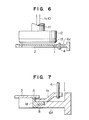
- Fig. 6 is a side view which shows an appearance of the substrate heating unit.
- a dish-shaped receiving tray 13 of quartz is removably attached to the bottom of a container 12 integrated with the cylindrical holder 11 so that the heater 3 irradiates heat rays toward the silicon substrate 2 through the tray 13 of the container 12.
- the second vacuum chamber 6b is equipped with gas nozzle 8 on the side wall thereof through which a nitrogen gas is introduced into the second vacuum chamber 6b as described later, and a nozzle port at the foremost end of the gas nozzle 8 is opened upwardly at the position above the intermediate part of the second vacuum chamber 6b.
- the substrate holder 1 serving to hold the silicon substrate 2 is designed in an annular configuration and has an inner stepped part 1 a and an outer stepped part 1 so as to hold the silicon substrate 2 around the inner stepped part l a.
- the first vacuum chamber 6a includes a plurality of support rods 4 of which lowermost ends are fixedly secured to the substrate holder 1, and the upper ends of the support rods 4 are inserted through guide holes 22a on a guide plate 22 which is fixed to the first vacuum chamber 6a via a suitable member (not shown).
- One of the support rods 4 extends upwardly through the upper wall of the first vacuum chamber 6a until it is operatively connected to a linear motion feedthrough 5.
- the support rod 4 is raised up or lowered and thereby the substrate holder 1 is raised up or lowered via the support rod 4.
- Fig. 1 shows the operative state that the substrate holder 1 having the silicon substrate 2 held thereon is raised up by actuation of the linear motion feedthrough 5 so that the first vacuum chamber 6a and the second vacuum chambeer 6b are gastightly isolated from each other by bringing the outer stepped part 1 b of the substrate holder 1 in close contact with the inner periphery of the rim 6c.
- the substrate holder 1 After a silicon film is formed on the silicon substrate 2 while a source gas (Si 2 He) is supplied into the second vacuum chamber 6b from the gas supplying means, the substrate holder 1 is lowered by actuation of the linear motion feedthrough 5. Then, the silicon substrate 2 held on the substrate holder 1 is taken out of the vacuum vessel 6 with the aid of a conveying arm (not shown) so that it is conveyed to a substrate exchanging room (not shown).
- a source gas Si 2 He
- a pressure in the first vacuum chamber 6a is equalized to a pressure in the second vacuum chamber 6b.
- conveying arm and the substrate exchanging chamber are arranged in the locations rearward or forward of the drawing plane as seen in Fig. 1.
- the present invention has been described above with respect to the embodiment wherein the vacuum vessel is constructed in a cylindrical configuration. However, the present invention should not be limited only to this configuration. Alternatively, the vacuum vessel may be constructed in other configuration.
- Fig. 2 is a graph which shows results derived from measurements conducted for a pressure difference between the pressure in the first vacuum chamber 6a and the pressure in the second vacuum chamber 6b in a case where a nitrogen gas is introduced into the second vacuum chamber 6b through the gas nozzle 8 serving as gas supplying means.
- small circle marks represent a case where measurements were conducted when the substrate is not heated, i.e., at a room temperature and X marks represent a case where measurements were conducted when the substrate is heated at a temperature of 900 ° C, wherein an ordinate designates the pressure in the first vacuum chamber 6a and an abscissa designates the pressure in the second vacuum chamber 6b.
- an evacuating speed of the turbo molecular pump 7 installed for the first vacuum chamber 6a is determined to be smaller than that of the turbo molecular pump 9 installed for the second vacuum chamber 6b.
- the pressure in the first vacuum chamber 6a is higher by double figures than that of the second vacuum chamber 6b. This means that an isolating effect derived by arrangement of the substrate 2 and the substrate holder 1 is remarkably high.
- Fig. 3 is a graph which shows results derived from measurements conducted for a relationship between the number of epitaxial growth cycle and the number of dust particles deposited on the surface of a substrate in a case where a silicon film is epitaxially grown when a disilane gas is used as a source gas.
- the substrate with which measurement were conducted in the above-described manner is a substrate practically used on a mass production line with a pattern formed thereon using an oxide film. The reason why such a substrate was used in that way consists in avoidance of adhesion of the substrate holder 1 to the substrate 2.
- small white circle marks represent results derived from measurements conducted for a relationship between the number of growth cycle and the number of dust particles in a case where a same material as that of the substrate, i.e., a silicon was used for the substrate holder 1 to gastightly isolate the first vacuum chamber 6a from the second vacuum chamber 6b
- small black circle marks represent results derived from measurement conducted for the same relationship as mentioned above for the purpose of comparison in a case where treatment was carried out under the same conditions as mentioned above except that a quartz was used as a material for the substrate holder 1 and the isolating member 6c in the form of an annular rim did not exist in the vacuum vessel 6, that is, the vacuum vessel 6 is not separated gastightly between the first and the second chambers.
- Fig. 3 shows that the number of dust particles rapidly increases when the number of silicon film growth cycle exceeds 140 in the case where a quartz was used as a material for the substrate holder 1 and the isolating member 6c did not exist in the vacuum vessel 6.
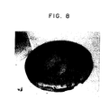
- Fig. 8 is a photograph which was taken with the tray 13 of quartz removed from the vacuum vessel 6 after silicon film growth cycle was repeated by 300 times in order to show the state visually observed on the surface of the tray 13.
- the silicon film is a different kind of material from that of the tray 13 of quartz, the silicon film is cracked due to a difference between an expansion coefficient of the silicon and an expansion coefficient of the quartz in the presence of a strain stress appearing between the different kinds of materials at every time of film formation, resulting in partial peeling of the silicon film being started.
- the kind of a growing film is same as the kind of a substrate on which the film is deposited, no stress is induced therebetween because the film is integrated homogenously with the substrate.
- the silicon film deposited on the substrate holder made of silicon is epitaxially grown, and the silicon film is then integrated homogeneously with the substrate holder. For this reason, there is no possibility that peeling takes place with the deposited film.
- Figs. 4(a) and 4(b) are graphs which show results derived from analyses conducted for a concentration of carbon in an epitaxially growing silicon film in the direction of a depth by employing a secondary ion mass spectrometry (SIMS) analyzing method.
- Fig. 4(a) is a graph which shows results derived in a case where the apparatus of the present invention including an isolating member is used for forming a silicon film
- Fig. 4(b) is a graph which likewise shows results derived in a case where a conventional apparatus including no isolating member is used for forming a silicon film, for the purpose of comparison.
- Fig. 7 is a fragmentary sectional view of a vacuum film forming apparatus in accordance with another embodiment of the present invention, particularly illustrating the structure of a substrate holder.
- the substrate holder is composed of a support ring 1 for supporting a substrate 2 and a carriage 1 for displacing the substrate 2 in the upward direction.
- the support ring 1 is placed on a rim 6d which serves in the same manner as the rim 6c which has been described above with reference to Fig. 1.
- a support rod 4 operatively connected to the carriage 1 e is raised or lowered in the same manner as the support rod 4 which has likewise been described above with reference to Fig. 1, by actuating the linear motion feedthrough 5 arranged outside of the vacuum vessel 6.
- th heating unit can also retreat upwardly.
- a contact portion A of the substrate 2 is brought in close contact with the upper surface of the support ring 1 by a dead weight of the substrate 2.
- a contact portion B of the support ring 1 d is likewise brought in close contact with the upper surface of the rim 6d by a dead weight of the support ring 1 in addition to the dead weight of the substrate 2.
- the vacuum film forming apparatus of the present invention is constructed such that the vacuum vessel is divided into two parts, i.e., a vacuum chamber on the heating unit side and a vacuum chamber on the treatment side and both of the vacuum chambers are isolated from each other with a substrate and a substrate holder interposed therebetween.
- both vacuum chambers are separately evacuated so as to produce a differential pressure therebetween. Consequently, the apparatus of the present invention offers the following advantageous effects:
- Fig. 5 is a graph which illustrates that a pressure in the first vacuum chamber 6a on the heater side and a pressure in the second vacuum chamber 6b on the treatment side vary as a flow rate of the disilane gas varies.
- the silicon substrate 2 is heated up to an elevated temperature of about 860 ° C with the aid of the heater 3.
- a silicon thin film is epitaxially grown on the silicon substrate 2.
- the pressure in the first vacuum chamber 6a of Fig. 5 is higher by three figures than that in the first vacuum chamber 6a of Fig. 2. This results from hydrogen molecule generated by pyrolysis of disilane molecule on the silicon substrate 2. It may be considered that hydrogen molecule can easily pass through a narrow gap, for example, a gap between the silicon substrate 2 and the substrate holder 1.
- the apparatus of the present invention has the following characterizing features by virtue of arrangement of evacuating means for the vacuum chamber including a heater.
Landscapes
- Chemical & Material Sciences (AREA)
- Chemical Kinetics & Catalysis (AREA)
- Engineering & Computer Science (AREA)
- Materials Engineering (AREA)
- Mechanical Engineering (AREA)
- Metallurgy (AREA)
- Organic Chemistry (AREA)
- General Chemical & Material Sciences (AREA)
- Chemical Vapour Deposition (AREA)
- Physical Vapour Deposition (AREA)
- Physical Deposition Of Substances That Are Components Of Semiconductor Devices (AREA)
- Crystals, And After-Treatments Of Crystals (AREA)
Applications Claiming Priority (2)
| Application Number | Priority Date | Filing Date | Title |
|---|---|---|---|
| JP253191/90 | 1990-09-21 | ||
| JP25319190 | 1990-09-21 |
Publications (2)
| Publication Number | Publication Date |
|---|---|
| EP0476480A1 true EP0476480A1 (de) | 1992-03-25 |
| EP0476480B1 EP0476480B1 (de) | 1995-07-26 |
Family
ID=17247818
Family Applications (1)
| Application Number | Title | Priority Date | Filing Date |
|---|---|---|---|
| EP91115234A Expired - Lifetime EP0476480B1 (de) | 1990-09-21 | 1991-09-10 | Vorrichtung zum Herstellen einer Schicht im Vacuum |
Country Status (5)
| Country | Link |
|---|---|
| US (1) | US5284521A (de) |
| EP (1) | EP0476480B1 (de) |
| KR (1) | KR950007966B1 (de) |
| CA (1) | CA2051214C (de) |
| DE (1) | DE69111540T2 (de) |
Cited By (4)
| Publication number | Priority date | Publication date | Assignee | Title |
|---|---|---|---|---|
| US5494494A (en) * | 1992-06-24 | 1996-02-27 | Anelva Corporation | Integrated module multi-chamber CVD processing system and its method for processing substrates |
| DE19847101C1 (de) * | 1998-10-13 | 2000-05-18 | Wacker Siltronic Halbleitermat | CVD-Reaktor und Verfahren zur Herstellung einer mit einer epitaktischen Schicht versehenen Halbleiterscheibe |
| US6579589B1 (en) | 1999-05-28 | 2003-06-17 | Wackersiltronic Gesellschaft Fur Halbleitermaterialien Ag | Semiconductor wafer with crystal lattice defects, and process for producing this semiconductor wafer |
| WO2005017980A1 (en) * | 2003-08-15 | 2005-02-24 | Infineon Technologies Ag | Methods and apparatus for processing semiconductor devices by gas annealing |
Families Citing this family (6)
| Publication number | Priority date | Publication date | Assignee | Title |
|---|---|---|---|---|
| JPH0811718B2 (ja) * | 1992-02-27 | 1996-02-07 | 大同ほくさん株式会社 | ガスソース分子線エピタキシー装置 |
| JP3604706B2 (ja) * | 1992-07-23 | 2004-12-22 | キヤノン株式会社 | 成膜方法 |
| KR100200705B1 (ko) * | 1996-06-08 | 1999-06-15 | 윤종용 | 반도체 디바이스 제조장치, 제조장치의 공정 조건 조절방법 및 이를 이용한 커패시터 제조방법 |
| US20060260938A1 (en) * | 2005-05-20 | 2006-11-23 | Petrach Philip M | Module for Coating System and Associated Technology |
| US20070256934A1 (en) * | 2006-05-08 | 2007-11-08 | Perata Michael R | Apparatus and Method for Coating Substrates With Approximate Process Isolation |
| TWI826001B (zh) * | 2022-09-19 | 2023-12-11 | 汎銓科技股份有限公司 | 一種減少缺陷的鍍膜方法 |
Citations (4)
| Publication number | Priority date | Publication date | Assignee | Title |
|---|---|---|---|---|
| US3156591A (en) * | 1961-12-11 | 1964-11-10 | Fairchild Camera Instr Co | Epitaxial growth through a silicon dioxide mask in a vacuum vapor deposition process |
| US3394678A (en) * | 1966-12-23 | 1968-07-30 | Air Reduction | Apparatus for vacuum coating |
| EP0319122A1 (de) * | 1987-11-30 | 1989-06-07 | Daidousanso Co., Ltd. | Vorrichtung und ihre Verwendung zur Herstellung von Halbleitern |
| US4895107A (en) * | 1987-07-06 | 1990-01-23 | Kabushiki Kaisha Toshiba | Photo chemical reaction apparatus |
Family Cites Families (9)
| Publication number | Priority date | Publication date | Assignee | Title |
|---|---|---|---|---|
| US4767251A (en) * | 1986-05-06 | 1988-08-30 | Amtech Systems, Inc. | Cantilever apparatus and method for loading wafer boats into cantilever diffusion tubes |
| JPS63238263A (ja) * | 1987-03-25 | 1988-10-04 | Seiko Epson Corp | 真空成膜装置のゴミ防止板 |
| FR2621930B1 (fr) * | 1987-10-15 | 1990-02-02 | Solems Sa | Procede et appareil pour la production par plasma de couches minces a usage electronique et/ou optoelectronique |
| JP2543961B2 (ja) * | 1987-11-30 | 1996-10-16 | 大同ほくさん株式会社 | 半導体製造装置 |
| JP2528165B2 (ja) * | 1987-11-30 | 1996-08-28 | 大同ほくさん株式会社 | 半導体製造装置 |
| JPH01257322A (ja) * | 1987-11-30 | 1989-10-13 | Daido Sanso Kk | 半導体の製造方法 |
| JP2612602B2 (ja) * | 1987-12-17 | 1997-05-21 | 東洋インキ製造 株式会社 | 連続蒸着フィルムの製造方法および装置 |
| US5104694A (en) * | 1989-04-21 | 1992-04-14 | Nippon Telephone & Telegraph Corporation | Selective chemical vapor deposition of a metallic film on the silicon surface |
| US5180432A (en) * | 1990-01-08 | 1993-01-19 | Lsi Logic Corporation | Apparatus for conducting a refractory metal deposition process |
-
1991
- 1991-09-04 US US07/754,522 patent/US5284521A/en not_active Expired - Lifetime
- 1991-09-10 DE DE69111540T patent/DE69111540T2/de not_active Expired - Lifetime
- 1991-09-10 EP EP91115234A patent/EP0476480B1/de not_active Expired - Lifetime
- 1991-09-10 KR KR1019910015794A patent/KR950007966B1/ko not_active Expired - Fee Related
- 1991-09-12 CA CA002051214A patent/CA2051214C/en not_active Expired - Fee Related
Patent Citations (4)
| Publication number | Priority date | Publication date | Assignee | Title |
|---|---|---|---|---|
| US3156591A (en) * | 1961-12-11 | 1964-11-10 | Fairchild Camera Instr Co | Epitaxial growth through a silicon dioxide mask in a vacuum vapor deposition process |
| US3394678A (en) * | 1966-12-23 | 1968-07-30 | Air Reduction | Apparatus for vacuum coating |
| US4895107A (en) * | 1987-07-06 | 1990-01-23 | Kabushiki Kaisha Toshiba | Photo chemical reaction apparatus |
| EP0319122A1 (de) * | 1987-11-30 | 1989-06-07 | Daidousanso Co., Ltd. | Vorrichtung und ihre Verwendung zur Herstellung von Halbleitern |
Non-Patent Citations (1)
| Title |
|---|
| PATENT ABSTRACTS OF JAPAN vol. 13, no. 39 (C-563)(3387) 27 January 1989 & JP-A-63 238 263 ( SEIKO EPSON CORP. ) 4 October 1988 * |
Cited By (6)
| Publication number | Priority date | Publication date | Assignee | Title |
|---|---|---|---|---|
| US5494494A (en) * | 1992-06-24 | 1996-02-27 | Anelva Corporation | Integrated module multi-chamber CVD processing system and its method for processing substrates |
| US5505779A (en) * | 1992-06-24 | 1996-04-09 | Anelva Corporation | Integrated module multi-chamber CVD processing system and its method for processing substrates |
| US5534072A (en) * | 1992-06-24 | 1996-07-09 | Anelva Corporation | Integrated module multi-chamber CVD processing system and its method for processing subtrates |
| DE19847101C1 (de) * | 1998-10-13 | 2000-05-18 | Wacker Siltronic Halbleitermat | CVD-Reaktor und Verfahren zur Herstellung einer mit einer epitaktischen Schicht versehenen Halbleiterscheibe |
| US6579589B1 (en) | 1999-05-28 | 2003-06-17 | Wackersiltronic Gesellschaft Fur Halbleitermaterialien Ag | Semiconductor wafer with crystal lattice defects, and process for producing this semiconductor wafer |
| WO2005017980A1 (en) * | 2003-08-15 | 2005-02-24 | Infineon Technologies Ag | Methods and apparatus for processing semiconductor devices by gas annealing |
Also Published As
| Publication number | Publication date |
|---|---|
| EP0476480B1 (de) | 1995-07-26 |
| CA2051214A1 (en) | 1992-03-22 |
| DE69111540T2 (de) | 1996-03-28 |
| KR950007966B1 (ko) | 1995-07-21 |
| US5284521A (en) | 1994-02-08 |
| KR920007126A (ko) | 1992-04-28 |
| CA2051214C (en) | 1998-11-24 |
| DE69111540D1 (de) | 1995-08-31 |
Similar Documents
| Publication | Publication Date | Title |
|---|---|---|
| KR100415475B1 (ko) | 기판 상에 박막을 성장시키는 장치 | |
| US4846102A (en) | Reaction chambers for CVD systems | |
| US4800105A (en) | Method of forming a thin film by chemical vapor deposition | |
| US7494545B2 (en) | Epitaxial deposition process and apparatus | |
| US7699934B2 (en) | Epitaxial wafer production apparatus and susceptor structure | |
| US5246536A (en) | Method for growing single crystal thin films of element semiconductor | |
| EP0259777A2 (de) | Verfahren zur Erzeugung von Einkristall-Dünnschichten aus Halbleitergrundstoff | |
| EP0870852A1 (de) | Vorrichtung und Verfahren zur Verhinderung von Kondensation in einer Abgasleitung | |
| EP0476480B1 (de) | Vorrichtung zum Herstellen einer Schicht im Vacuum | |
| KR20010034128A (ko) | 화학 기상 증착 냉벽 챔버 및 배출 라인의 세정 방법 | |
| US5261960A (en) | Reaction chambers for CVD systems | |
| EP0164928A2 (de) | Senkrechter Heisswandreaktor zur chemischen Abscheidung aus der Gasphase | |
| GB2282825A (en) | Chemical vapour deposition apparatus | |
| US6334901B1 (en) | Apparatus for forming semiconductor crystal | |
| US4661199A (en) | Method to inhibit autodoping in epitaxial layers from heavily doped substrates in CVD processing | |
| US6279506B1 (en) | Reactor for coating plane substrates and method for producing said substrates | |
| US3341374A (en) | Process of pyrolytically growing epitaxial semiconductor layers upon heated semiconductor substrates | |
| US5076207A (en) | Apparatus for atmospheric chemical vapor deposition | |
| JP2983084B2 (ja) | 薄膜形成方法および、この方法を用いた真空成膜装置 | |
| US4895737A (en) | Metal-organic chemical vapor deposition | |
| JPH02208925A (ja) | 半導体膜の形成方法 | |
| US5154773A (en) | Vapor phase epitaxial growth apparatus having exhaust unit for removing unwanted deposit | |
| JPS63166215A (ja) | 半導体気相成長装置 | |
| Jagannathan et al. | Hydrogen beam stimulated low‐temperature dissociation of organometallics—application for lowering the growth temperature in a metalorganic chemical vapor deposition process | |
| JP2656029B2 (ja) | 結晶成長装置 |
Legal Events
| Date | Code | Title | Description |
|---|---|---|---|
| PUAI | Public reference made under article 153(3) epc to a published international application that has entered the european phase |
Free format text: ORIGINAL CODE: 0009012 |
|
| AK | Designated contracting states |
Kind code of ref document: A1 Designated state(s): DE GB NL |
|
| 17P | Request for examination filed |
Effective date: 19920403 |
|
| 17Q | First examination report despatched |
Effective date: 19940411 |
|
| GRAA | (expected) grant |
Free format text: ORIGINAL CODE: 0009210 |
|
| AK | Designated contracting states |
Kind code of ref document: B1 Designated state(s): DE GB NL |
|
| REF | Corresponds to: |
Ref document number: 69111540 Country of ref document: DE Date of ref document: 19950831 |
|
| PLBE | No opposition filed within time limit |
Free format text: ORIGINAL CODE: 0009261 |
|
| STAA | Information on the status of an ep patent application or granted ep patent |
Free format text: STATUS: NO OPPOSITION FILED WITHIN TIME LIMIT |
|
| 26N | No opposition filed | ||
| REG | Reference to a national code |
Ref country code: GB Ref legal event code: IF02 |
|
| PGFP | Annual fee paid to national office [announced via postgrant information from national office to epo] |
Ref country code: NL Payment date: 20090915 Year of fee payment: 19 Ref country code: GB Payment date: 20090909 Year of fee payment: 19 |
|
| PGFP | Annual fee paid to national office [announced via postgrant information from national office to epo] |
Ref country code: DE Payment date: 20090903 Year of fee payment: 19 |
|
| REG | Reference to a national code |
Ref country code: NL Ref legal event code: V1 Effective date: 20110401 |
|
| GBPC | Gb: european patent ceased through non-payment of renewal fee |
Effective date: 20100910 |
|
| REG | Reference to a national code |
Ref country code: DE Ref legal event code: R119 Ref document number: 69111540 Country of ref document: DE Effective date: 20110401 |
|
| PG25 | Lapsed in a contracting state [announced via postgrant information from national office to epo] |
Ref country code: DE Free format text: LAPSE BECAUSE OF NON-PAYMENT OF DUE FEES Effective date: 20110401 |
|
| PG25 | Lapsed in a contracting state [announced via postgrant information from national office to epo] |
Ref country code: GB Free format text: LAPSE BECAUSE OF NON-PAYMENT OF DUE FEES Effective date: 20100910 Ref country code: NL Free format text: LAPSE BECAUSE OF NON-PAYMENT OF DUE FEES Effective date: 20110401 |