EP0476136A1 - Unite electronique tridimensionnelle et son procede de fabrication - Google Patents
Unite electronique tridimensionnelle et son procede de fabrication Download PDFInfo
- Publication number
- EP0476136A1 EP0476136A1 EP90915983A EP90915983A EP0476136A1 EP 0476136 A1 EP0476136 A1 EP 0476136A1 EP 90915983 A EP90915983 A EP 90915983A EP 90915983 A EP90915983 A EP 90915983A EP 0476136 A1 EP0476136 A1 EP 0476136A1
- Authority
- EP
- European Patent Office
- Prior art keywords
- carrier
- module
- electronic components
- carriers
- electronic component
- Prior art date
- Legal status (The legal status is an assumption and is not a legal conclusion. Google has not performed a legal analysis and makes no representation as to the accuracy of the status listed.)
- Withdrawn
Links
Images


Classifications
-
- H—ELECTRICITY
- H01—ELECTRIC ELEMENTS
- H01L—SEMICONDUCTOR DEVICES NOT COVERED BY CLASS H10
- H01L23/00—Details of semiconductor or other solid state devices
- H01L23/48—Arrangements for conducting electric current to or from the solid state body in operation, e.g. leads, terminal arrangements ; Selection of materials therefor
- H01L23/488—Arrangements for conducting electric current to or from the solid state body in operation, e.g. leads, terminal arrangements ; Selection of materials therefor consisting of soldered or bonded constructions
- H01L23/498—Leads, i.e. metallisations or lead-frames on insulating substrates, e.g. chip carriers
- H01L23/49811—Additional leads joined to the metallisation on the insulating substrate, e.g. pins, bumps, wires, flat leads
-
- H—ELECTRICITY
- H01—ELECTRIC ELEMENTS
- H01L—SEMICONDUCTOR DEVICES NOT COVERED BY CLASS H10
- H01L23/00—Details of semiconductor or other solid state devices
- H01L23/48—Arrangements for conducting electric current to or from the solid state body in operation, e.g. leads, terminal arrangements ; Selection of materials therefor
- H01L23/488—Arrangements for conducting electric current to or from the solid state body in operation, e.g. leads, terminal arrangements ; Selection of materials therefor consisting of soldered or bonded constructions
- H01L23/498—Leads, i.e. metallisations or lead-frames on insulating substrates, e.g. chip carriers
- H01L23/49805—Leads, i.e. metallisations or lead-frames on insulating substrates, e.g. chip carriers the leads being also applied on the sidewalls or the bottom of the substrate, e.g. leadless packages for surface mounting
-
- H—ELECTRICITY
- H01—ELECTRIC ELEMENTS
- H01L—SEMICONDUCTOR DEVICES NOT COVERED BY CLASS H10
- H01L23/00—Details of semiconductor or other solid state devices
- H01L23/52—Arrangements for conducting electric current within the device in operation from one component to another, i.e. interconnections, e.g. wires, lead frames
- H01L23/538—Arrangements for conducting electric current within the device in operation from one component to another, i.e. interconnections, e.g. wires, lead frames the interconnection structure between a plurality of semiconductor chips being formed on, or in, insulating substrates
- H01L23/5385—Assembly of a plurality of insulating substrates
-
- H—ELECTRICITY
- H01—ELECTRIC ELEMENTS
- H01L—SEMICONDUCTOR DEVICES NOT COVERED BY CLASS H10
- H01L25/00—Assemblies consisting of a plurality of individual semiconductor or other solid state devices ; Multistep manufacturing processes thereof
- H01L25/03—Assemblies consisting of a plurality of individual semiconductor or other solid state devices ; Multistep manufacturing processes thereof all the devices being of a type provided for in the same subgroup of groups H01L27/00 - H01L33/00, or in a single subclass of H10K, H10N, e.g. assemblies of rectifier diodes
- H01L25/04—Assemblies consisting of a plurality of individual semiconductor or other solid state devices ; Multistep manufacturing processes thereof all the devices being of a type provided for in the same subgroup of groups H01L27/00 - H01L33/00, or in a single subclass of H10K, H10N, e.g. assemblies of rectifier diodes the devices not having separate containers
- H01L25/065—Assemblies consisting of a plurality of individual semiconductor or other solid state devices ; Multistep manufacturing processes thereof all the devices being of a type provided for in the same subgroup of groups H01L27/00 - H01L33/00, or in a single subclass of H10K, H10N, e.g. assemblies of rectifier diodes the devices not having separate containers the devices being of a type provided for in group H01L27/00
- H01L25/0657—Stacked arrangements of devices
-
- H—ELECTRICITY
- H01—ELECTRIC ELEMENTS
- H01L—SEMICONDUCTOR DEVICES NOT COVERED BY CLASS H10
- H01L2225/00—Details relating to assemblies covered by the group H01L25/00 but not provided for in its subgroups
- H01L2225/03—All the devices being of a type provided for in the same subgroup of groups H01L27/00 - H01L33/648 and H10K99/00
- H01L2225/04—All the devices being of a type provided for in the same subgroup of groups H01L27/00 - H01L33/648 and H10K99/00 the devices not having separate containers
- H01L2225/065—All the devices being of a type provided for in the same subgroup of groups H01L27/00 - H01L33/648 and H10K99/00 the devices not having separate containers the devices being of a type provided for in group H01L27/00
- H01L2225/06503—Stacked arrangements of devices
- H01L2225/06524—Electrical connections formed on device or on substrate, e.g. a deposited or grown layer
-
- H—ELECTRICITY
- H01—ELECTRIC ELEMENTS
- H01L—SEMICONDUCTOR DEVICES NOT COVERED BY CLASS H10
- H01L2225/00—Details relating to assemblies covered by the group H01L25/00 but not provided for in its subgroups
- H01L2225/03—All the devices being of a type provided for in the same subgroup of groups H01L27/00 - H01L33/648 and H10K99/00
- H01L2225/04—All the devices being of a type provided for in the same subgroup of groups H01L27/00 - H01L33/648 and H10K99/00 the devices not having separate containers
- H01L2225/065—All the devices being of a type provided for in the same subgroup of groups H01L27/00 - H01L33/648 and H10K99/00 the devices not having separate containers the devices being of a type provided for in group H01L27/00
- H01L2225/06503—Stacked arrangements of devices
- H01L2225/06527—Special adaptation of electrical connections, e.g. rewiring, engineering changes, pressure contacts, layout
-
- H—ELECTRICITY
- H01—ELECTRIC ELEMENTS
- H01L—SEMICONDUCTOR DEVICES NOT COVERED BY CLASS H10
- H01L2225/00—Details relating to assemblies covered by the group H01L25/00 but not provided for in its subgroups
- H01L2225/03—All the devices being of a type provided for in the same subgroup of groups H01L27/00 - H01L33/648 and H10K99/00
- H01L2225/04—All the devices being of a type provided for in the same subgroup of groups H01L27/00 - H01L33/648 and H10K99/00 the devices not having separate containers
- H01L2225/065—All the devices being of a type provided for in the same subgroup of groups H01L27/00 - H01L33/648 and H10K99/00 the devices not having separate containers the devices being of a type provided for in group H01L27/00
- H01L2225/06503—Stacked arrangements of devices
- H01L2225/06551—Conductive connections on the side of the device
-
- H—ELECTRICITY
- H01—ELECTRIC ELEMENTS
- H01L—SEMICONDUCTOR DEVICES NOT COVERED BY CLASS H10
- H01L2225/00—Details relating to assemblies covered by the group H01L25/00 but not provided for in its subgroups
- H01L2225/03—All the devices being of a type provided for in the same subgroup of groups H01L27/00 - H01L33/648 and H10K99/00
- H01L2225/04—All the devices being of a type provided for in the same subgroup of groups H01L27/00 - H01L33/648 and H10K99/00 the devices not having separate containers
- H01L2225/065—All the devices being of a type provided for in the same subgroup of groups H01L27/00 - H01L33/648 and H10K99/00 the devices not having separate containers the devices being of a type provided for in group H01L27/00
- H01L2225/06503—Stacked arrangements of devices
- H01L2225/06572—Auxiliary carrier between devices, the carrier having an electrical connection structure
-
- H—ELECTRICITY
- H01—ELECTRIC ELEMENTS
- H01L—SEMICONDUCTOR DEVICES NOT COVERED BY CLASS H10
- H01L2225/00—Details relating to assemblies covered by the group H01L25/00 but not provided for in its subgroups
- H01L2225/03—All the devices being of a type provided for in the same subgroup of groups H01L27/00 - H01L33/648 and H10K99/00
- H01L2225/04—All the devices being of a type provided for in the same subgroup of groups H01L27/00 - H01L33/648 and H10K99/00 the devices not having separate containers
- H01L2225/065—All the devices being of a type provided for in the same subgroup of groups H01L27/00 - H01L33/648 and H10K99/00 the devices not having separate containers the devices being of a type provided for in group H01L27/00
- H01L2225/06503—Stacked arrangements of devices
- H01L2225/06579—TAB carriers; beam leads
-
- H—ELECTRICITY
- H01—ELECTRIC ELEMENTS
- H01L—SEMICONDUCTOR DEVICES NOT COVERED BY CLASS H10
- H01L2225/00—Details relating to assemblies covered by the group H01L25/00 but not provided for in its subgroups
- H01L2225/03—All the devices being of a type provided for in the same subgroup of groups H01L27/00 - H01L33/648 and H10K99/00
- H01L2225/04—All the devices being of a type provided for in the same subgroup of groups H01L27/00 - H01L33/648 and H10K99/00 the devices not having separate containers
- H01L2225/065—All the devices being of a type provided for in the same subgroup of groups H01L27/00 - H01L33/648 and H10K99/00 the devices not having separate containers the devices being of a type provided for in group H01L27/00
- H01L2225/06503—Stacked arrangements of devices
- H01L2225/06582—Housing for the assembly, e.g. chip scale package [CSP]
-
- H—ELECTRICITY
- H01—ELECTRIC ELEMENTS
- H01L—SEMICONDUCTOR DEVICES NOT COVERED BY CLASS H10
- H01L2225/00—Details relating to assemblies covered by the group H01L25/00 but not provided for in its subgroups
- H01L2225/03—All the devices being of a type provided for in the same subgroup of groups H01L27/00 - H01L33/648 and H10K99/00
- H01L2225/04—All the devices being of a type provided for in the same subgroup of groups H01L27/00 - H01L33/648 and H10K99/00 the devices not having separate containers
- H01L2225/065—All the devices being of a type provided for in the same subgroup of groups H01L27/00 - H01L33/648 and H10K99/00 the devices not having separate containers the devices being of a type provided for in group H01L27/00
- H01L2225/06503—Stacked arrangements of devices
- H01L2225/06589—Thermal management, e.g. cooling
-
- H—ELECTRICITY
- H01—ELECTRIC ELEMENTS
- H01L—SEMICONDUCTOR DEVICES NOT COVERED BY CLASS H10
- H01L2924/00—Indexing scheme for arrangements or methods for connecting or disconnecting semiconductor or solid-state bodies as covered by H01L24/00
- H01L2924/0001—Technical content checked by a classifier
- H01L2924/0002—Not covered by any one of groups H01L24/00, H01L24/00 and H01L2224/00
-
- H—ELECTRICITY
- H01—ELECTRIC ELEMENTS
- H01L—SEMICONDUCTOR DEVICES NOT COVERED BY CLASS H10
- H01L2924/00—Indexing scheme for arrangements or methods for connecting or disconnecting semiconductor or solid-state bodies as covered by H01L24/00
- H01L2924/10—Details of semiconductor or other solid state devices to be connected
- H01L2924/11—Device type
- H01L2924/12—Passive devices, e.g. 2 terminal devices
- H01L2924/1204—Optical Diode
- H01L2924/12044—OLED
Definitions
- the present invention relates to the assembly of electronic assemblies and devices using encapsulated and housing-free electronic components and relates in particular to a three-dimensional electronic component and a method for its production.
- a construction of a three-dimensional electronic component (GB, A, 2095039A) which contains electronic components which are accommodated in carriers (GB, A, 2127217A) which are provided with connecting contacts on the circumference and are arranged parallel to one another in the component, which is equipped with means for heat dissipation and with means for wiring the carrier via the side faces of the module.
- the carriers are made in the form of plates from a thermally conductive insulating material, on the surface of which the connection contacts lie. Electronic components without housings are fastened in the carriers, which are guided to the connection contacts of the carriers with the aid of spatial conductors, the carriers being connected to the walls of the module by means of sliding contacts.
- Each carrier is individually hermetically sealed with a lid or by potting a compound. Cables are laid in the walls of the block, which ensure that the beams are connected in parallel. Contacts can be used as lines, which are arranged in the walls of the block. The beams are spaced apart, and windows and ribs are provided in the walls of the building block to ensure air cooling. Every carrier can take part in the Repairs can be removed by removing one or more walls of the block.
- the module is connected to external devices by means of connections which are arranged on the end supports.
- the method for producing a three-dimensional electronic module in accordance with the aforementioned GB-PS comprises the production of the carriers, the arrangement of the electronic components in the carrier, the electrical connection of the components to the connection contacts of the carrier, the parallel arrangement of the carriers in the module, the wiring of the carriers over the side faces of the block.
- the crystals are fixed in the carriers either by brazing with braze or by gluing with an adhesive made of polymer from the back of the crystal.
- connection of the component to the connection contacts of the carrier by welding with wire connections is always a gradual and relatively unreliable process, which has a negative effect on the work intensity and reliability of the electronic devices.
- the invention has for its object to provide a three-dimensional electronic module with such an arrangement of electronic components and such wiring of the latter in three-dimensional space and with such an organization of heat dissipation that allow to shorten the length of the conductors connecting the components and a To facilitate facilitated heat retention of the device, as well as to create a method for the production of the electronic device, in which all operations are carried out in groups, what allows to ensure the reproducibility of the technical characteristics of the module and to reduce the manufacturing costs.
- the object is achieved in that in the three-dimensional electronic component, which contains electronic components, which are accommodated in carriers, which are provided on the circumference with connecting contacts and are arranged parallel to one another in the component, with means for heat dissipation and with means for wiring the carrier is equipped over the side surfaces of the module, according to the invention when housing-free electronic components are used in the module, these are arranged in a mutually oriented manner and also have an insulating layer in the current-conducting zones in addition to contact surfaces, moreover on the surface of the carrier and the electronic components Conductors are attached which connect the electronic components to one another and / or to the connection contacts and the carriers in the module, the module having on its surface means for firmly wiring the carriers to one another, w While each carrier has at least one connection which goes to the surface of the module and serves as the external connection of the module, the means for heat dissipation being in the form of heat-conducting ribs arranged directly in the heating zones and a heat dissipation element, the module being enclosed in
- the housing-free electronic components in the module When using the housing-free electronic components in the module, they are fastened in an oriented manner in the supports, which makes it possible to ensure an identity of the construction of an apparatus during its series production and to proceed in groups during its assembly, for example vacuum evaporation of metal layers by "free"" Realize mask. All current-conducting zones of the components, apart from the contact areas, are protected by an insulating layer in order to prevent contact with the conductors and other components during the manufacture and operation of the apparatus.
- the conductors are applied to the surface of the components and carriers, which makes the construction more compact, more resistant to mechanical and thermal influences, and allows assembly to be carried out in groups.
- the design of such carriers is easily automated using mathematical methods that are accepted in the wiring of conventional printed circuit boards.
- the surface of the module is connected by one-piece (but detachable) means, for example by soldering the connections between the carriers. This considerably increases the reliability of the connections, while the arrangement of the contacts on the outer surface of the module permits a quality check of the connections and, if necessary, their restoration.
- Each carrier has connections that appear as external connections of the module, which is why all external connections lie along the surface of the module, which significantly reduces the length of the interconnections within the module and makes the construction more compact.
- the heat-conducting ribs are arranged directly in the heating zones and have thermal contact with the heat dissipation element. This makes it possible to ensure more optimal temperature conditions for the work of each component and the apparatus as a whole, and leads to a considerable reduction in their size and mass.
- the entire module has a uniform hermitizing shell, which is justified in this type of apparatus because it is installed in the module Careful control and training of each component as part of the carrier must precede as well as the component must be allowed to work for a while before it is hermetically sealed.
- connection contacts of the carriers are made in the form of solid metal beams. This simplifies contacting the wearer during the control and training process.
- At least one carrier together with the electronic components attached to it is manufactured in the form of a monolithic construction, the electronic components and the carrier made of polymeric material having a uniform front surface. This allows the amount of carriers to be manufactured in groups at the same time.
- the insulating layer on the carriers is produced in the form of a partial application to the front of the electronic components from the polymeric material of the carrier. This makes it possible to protect the current-conducting zones of the components at the same time as the carrier is being manufactured, which simplifies the technology of its production under the conditions of small series and one-off production.
- the insulating layer on the carriers can be produced in the form of a thin dielectric layer which is applied to the surfaces of the electronic components and the carriers. This can be used in the case of a dense arrangement of the contact surfaces on the electronic components and in the application of the conductors in processes in which a high flatness of the surface of the product is necessary, and in the case of large series and mass production.
- At least one carrier is produced in the form of a flexible printed circuit board fastened to the outer frame of the carrier with a wiring forming the outer connection contacts on the front, front and rear surface of the carrier.
- the plate is bent around the outer frame and forms the connection contacts of the carrier.
- At least one of the beams consists of individual parts that are electrically and mechanically connected via contacts lying on their surfaces.
- the carriers When using a large number of components of different sizes, it is desirable for the carriers to be provided with plates which are made from a material with a high thermal conductivity and in which the electronic components are accommodated. This facilitates temperature control during the work of the electronic components and increases the reliability of the devices.
- the three-dimensional electronic component which contains electronic components that are accommodated in carriers, which on the circumference with connection contacts provided and arranged parallel to each other in the module, which is equipped with means for heat dissipation and with means for wiring the carrier via the side surfaces of the module, according to the invention has at least one electronic component enclosed in a housing serving as a carrier, with on the surface of the module means for firmly wiring the connections of the carriers to one another, while each encapsulated electronic component has at least one connection going to the surface of the module and serving as its external connection, the means for heat dissipation in the form of heat-conducting ribs arranged directly in the heating zones and a heat dissipation element, wherein the module is enclosed in a hermetic envelope.
- the three-dimensional electronic component which contains electronic components which are accommodated in carriers, which are provided on the circumference with connecting contacts and are arranged parallel to one another in the component, with means for heat dissipation and with means for wiring the carrier is equipped over the side faces of the building blocks
- the housing-less electronic components and at least one electronic component enclosed in a housing serving as a carrier
- the housing-free electronic components being arranged in the carriers oriented in relation to one another and in the current-conducting zones except Contact surfaces also have an insulating layer
- conductors are attached to the surface of the carrier and the housing-free electronic components, which connect the electronic components to each other and / or to the connection contacts of the carrier and the carrier in the module, the module on its surface via means for firmly wiring the carrier and the encapsulated electronic components to one another
- each carrier and each encapsulated electronic component has at least one connector which goes to the surface of the module and serves as its external connector, the means for dissipating heat being arranged in
- the means for the hard wiring of the supports contain at least one printed circuit board which is connected to the connection contacts of the supports, which are attached to the end faces of the latter. and / or is connected to the connections of the encapsulated electronic components. This allows the packing density to be increased.
- the means for hard wiring the carrier is in the form of conductors which are directly on the surface of the module with partial coverage of the connection contacts of the carrier and / or the connections of the encapsulated electronic components are applied.
- the means for hard wiring the carrier is in the form of at least one printed circuit board and of conductors separated from one another by an insulating layer, the conductors being intended to lie on the surface of the module.
- the means for firmly wiring the carriers is in the form of individual spatial conductors arranged above the surface of the module.
- the electronic component prefferably has at least one surface which has thermal contact with the means for heat dissipation.
- the thermal contact of an electronic component with the means for heat dissipation is ensured over any surface thereof, including the end faces. This considerably facilitates heat conduction in the work of the component and the component as a whole and consequently increases the reliability of the construction.
- the object is also achieved in that in the process for producing a three-dimensional electronic component which arranges the electronic components in the carrier, an electrical connection of the electronic components to the connection contacts of the carrier, a parallel arrangement of the carriers in the component, the wiring of the carriers encompassed over the side surfaces of the block,
- housing-free electronic components when housing-free electronic components are used in the component, these are previously grouped according to the principle of a minimum number of connection contacts on the carrier, the electronic components are aligned with one another and temporarily fixed, the carriers are manufactured with a final fastening of the electronic components in them, and the unprotected current-carrying components Zones of the electronic components apart from the contact surfaces are electrically insulated, the contact surfaces of the electronic components and the connection contacts of the carrier are cleaned of organic dirt and oxide layers, conductors are applied to the surfaces of the electronic components and the carrier, the connection contacts of the carriers are electrically connected on the surface of the module the assembled component is hermetically sealed.
- the object is also achieved in that in the process for producing a three-dimensional electronic component which arranges the electronic components in the carrier, an electrical connection of the electronic components to the connection contacts of the carrier, a parallel arrangement of the carriers in the component, the wiring of the carriers
- housing-free electronic components when housing-free electronic components are used in the component, these are grouped over the side surfaces of the component beforehand according to the principle of a minimum number of connection contacts on the carrier, the unprotected current-conducting zones of the electronic components are isolated apart from the contact surfaces, the electronic components are aligned with one another and provisionally fixed, the carrier with a final attachment of the electronic components manufactured in them, the contact surfaces of the electronic components and the connection contacts of the carrier of organic dirt and oxide layers cleaned, applied to the surfaces of the electronic components and the carrier conductors, the connection contacts of the carriers are electrically connected on the surface of the module, the assembled module is hermetically sealed.
- the previous grouping of the electronic components according to the principle of a minimum possible number of contacts in the carrier ensures the arrangement of several components with a maximum number of connections between the components in the carrier.
- the orientation of the components and their provisional fixation make it possible to improve the errors permitted in the arrangement of the components by carrying out a check.
- the production of the carrier with the final fastening of the components using polymeric materials by casting or pressing ensures a low workload in the production of the carrier.
- the isolation of the unprotected current-conducting zones in the components, which is carried out in groups either at the same time as the carrier is manufactured or by applying insulation layers, is aimed at increasing the reliability of the product.
- the cleaning of the contact surfaces of the components from the organic contaminants and the oxide layers makes it possible to avoid the contaminations in the area of the connection of the conductor to the contact surface of the component, which lead to corrosion, and to ensure reliable electrical contact at the connection point.
- the electrical connection of the connection contacts of the carriers on the surface of the component allows a large amount of the conductors to be applied simultaneously using highly productive processes (for example by vacuum evaporation of conductors using "free" masks), the small amount The thickness of the conductor makes the carrier compact. This results in a reduction in the size and mass of the carrier and the labor intensity in its manufacture.
- Hermetically sealing the module with, for example, a low-temperature potting compound ensures normal functioning of the module in various climatic conditions.
- housing-free electronic components are aligned with one another according to their contact surfaces in optical processes.
- the housing-free electronic components it is expedient for the housing-free electronic components to be oriented towards one another according to their contours.
- the components are oriented according to the contour if the required accuracy and reproducibility of the dimensions of the components are ensured.
- This variant of the operation is highly productive, but can only be used on components with large contact areas (of the type of ohmic resistors or capacitors).
- the electronic components are temporarily fixed by gluing with the front to an adhesive layer that is applied to a flexible polymer film.
- an adhesive layer is applied to the front of the electronic components and the electronic components are temporarily fixed to a flexible polymeric film by gluing them to the front.
- the electronic components are first fixed by arranging them in the windows of a template and then pressed with the contact surfaces against an elastic coating applied to a flat plate until they have been attached as part of the carrier.
- the provisional fixation of the electronic components and, if applicable, the metal frame acting as a connection by gluing them to the front on the flexible polymer film with subsequent removal of the adhesive from the exposed parts of the film and from the front surfaces of the electronic components after the film has been removed is used for components with small contact areas (integrated circuit type) used to ensure their fixation with greater accuracy.
- the arrangement of the electronic components in the windows of the template or with the help of vacuum pressure with subsequent mechanical pressing of their contact surfaces on the flat elastic base plate until they have been attached as part of the carrier, allows the components to be glued with subsequent removal of the Prevent adhesive layer, and is applicable for components with a good reproducibility of the dimensions and the arrangement of the contact surfaces.
- the final fastening of the electronic components is expediently carried out by means of a polymeric material with a linear thermal expansion coefficient which is adapted to the material of the substrate. This allows the scope of the construction of the three-dimensional electronic module in question to be expanded.
- connection contacts it is expedient for the conductors to be applied to the contact surfaces of the electronic components and the carrier while at the same time forming its connection contacts.
- the simultaneous application of the connection contacts together with the conductors is possible, for example, with vacuum deposition of the conductors. This significantly reduces the amount of work involved in manufacturing the carriers by excluding the contact frame from their construction.
- connection contacts of the carrier which are in the form of solid metal bars, are bent in such a way that the electrical contact between the connections of the adjacent carriers is secured under their subsequent soldering during assembly of the module. This leads to a reduction in the amount of work involved in replacing the carriers when they are used in the construction of the module with regular wiring.
- the carriers having the connection contacts on the front and rear are arranged at a distance when they are arranged in the module and are soldered using a capillary effect, as a result of which a mechanical and electrical connection is established.
- the construction of the electronic component according to the invention can be easily removed before it has been completely hermetically sealed.
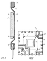
- the three-dimensional electronic component according to the invention contains carrier 1 (FIG. 1) in which electronic components, for example a crystal 2 of an integrated circuit, housing-free resistors 3, which are encapsulated by a polymeric material 4 together with fixed connection contacts 5.
- carrier 1 FOG. 1
- electronic components for example a crystal 2 of an integrated circuit, housing-free resistors 3, which are encapsulated by a polymeric material 4 together with fixed connection contacts 5.
- the current-conducting zones of the crystal 2 are through an insulating layer 6 in the form of applications of the polymer Materials 4 protected.
- Conductors 7 are applied to the surfaces of the crystal 2, the resistors 3 and the carrier 1, which interconnect the components with one another and with the connection contacts 5 and also serve to connect the carriers 1 to one another after their installation in the module.
- connection contacts 5 are carried out simultaneously with the conductors 7, as a result of which external connections I0 are formed, which are applied to the front, front and rear of the carrier 1. If the crystals 2 (FIG.
- the carrier 1 is designed in the form of a flexible printed circuit board 12 which is connected to the connection contacts 5 on an outer frame 13 is attached.
- a rigid attachment of the electronic components to the carrier 1 can be omitted: the crystal 2 is electrically connected to the wiring 11 by means of contact surfaces 14.
- One of the carriers 1 can consist of individual parts 15 which are connected to one another via contacts 16 located on their surfaces, for example with the aid of a solder.
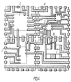
- the hatching is indicated conventionally in FIG. 4.
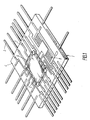
- the carriers 1 (FIG. 5) are arranged parallel to one another. Over the surfaces of the block the carriers 1 are electrically connected by conductors 17, which are applied to a flexible printed circuit board 18, whereby an optional wiring over the surfaces of the module is made possible.
- the extended contacts 5 of the carrier 1 are opened after covering them with a sheath 19 and additional conductors 20 are applied to the surface of the module.
- the module is then finally hermetically sealed by covering it with a polymeric shell 21.
- the construction of the module provides for the direct introduction of heat-conducting ribs 22 with a heat dissipation element 23 of the means for heat dissipation into the heating zones.
- the module is mechanically connected to a common cooling system 24, while the external connection contacts 5 of the carrier 1 maintain contact with a common circuit board 25, as a result of which external connections of the module are formed.
- the carrier 1 (FIG. 6) can be connected to one another in the module by casting with a polymeric material 26, by opening the end faces of the connections of the carrier 1, by applying conductors 20 to the surface of the module. In this case, the conductors 20 can be displaced somewhat against the end faces of the connections of the carrier 1. In the subsequent tinning, the connection between the conductor 20 and the contact 5 of the carrier 1 is duplicated by soldering, which increases the security of the connection.
- the carrier 1 (FIG. 7) can be connected in the module by spatial conductors 27.
- the spatial conductors 27 of a given configuration are placed on the protruding contacts 5 of the carriers 1 and connected to them electrically, for example by soldering.
- the sections are mechanically removed from its vicinity, the Carrier 1 replaced and the device restored by soldering reserve conductors 27 of the same configuration.
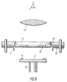
- the carrier 1 (Fig. 8) can be connected in the module through the connection contacts 5, which are designed in the form of solid metal beams.
- the contacts 5 are initially bent in such a way that their contact with the adjacent carrier 1 is ensured during assembly of the module.
- the carriers 1 are at a distance from one another with the connection contacts 5 applied to the front, front and back of the carrier 1.
- group soldering for example wave soldering
- a molten solder 28 penetrates into the gap between the carriers 1 due to the capillary effect and connects the connection contacts 5 of the adjacent carriers 1 to one another. If an exchange of the carrier 1 is required, the zone of its contact with the neighboring carriers 1 is locally heated to the melting temperature of the solder 28, the carrier 1 is exchanged for an intact one, and the soldering is repeated.
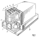
- the crystal 2 belonging to the carrier 1 has direct thermal contact with the heat dissipation element 23 via at least one surface 29.
- the special feature of the construction mentioned is that the conductors 7 are applied to an insulating layer are covering the front surface of the crystal 2.
- the construction of the mentioned module provides for the presence of an intermediate circuit board 30 with planar external connections 31.
- the module is hermetically sealed by a polymeric shell 21.
- the carriers 1 (FIG. 11) are provided with plates 32 made of a material with high thermal conductivity.
- the crystal maintains thermal contact with this plate 32, which occurs as a heat dissipation element within the carrier 1.
- This is particularly effective when using heat-generating electronic components of different sizes. In this case, favorable conditions for heat flow conduction along the block are created with little loss.
- the heat-conducting ribs 22 can be arranged to be quite leaky, which increases the packing density.
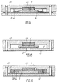
- a window 33 with an exposed part of the printed circuit board 18 is made in the sealed module. If necessary, the spatial conductors 27 or the encapsulated components are soldered onto the protruding contacts 5 of the carrier 1 which are guided through the plate 18. A mechanical interruption of the existing conductors 17 is also possible.
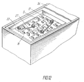
- the window 33 is closed by a cover 34 (FIG. 12).
- the housing of any encapsulated components with planar or axial connections can be used as carrier 1 in the module.
- the method according to the invention for producing a three-dimensional electronic module takes place as follows.
- the electronic components are grouped according to the principle of the minimum number of external connections for carrier 1 and the maintenance of the required functional capabilities with a limited number of type elements. This further allows the assembly process to be easily automated and the product to have high operating properties.
- a method is used which is based on the coincidence of the contact surfaces 14 (FIG. 13) of the component with a prefabricated mask or template 35.
- the component for example the crystal 2
- the mask or template 35 which has openings, is attached to a template holder 37, for example with the aid of a permanent magnet.
- a frame 38 with the connection contacts 5 is arranged on the template holder 37, which is previously glued to an adhesive layer applied to a transparent film 39.
- the crystal 2 is glued to the front of the film 39 and heated until the adhesive layer on the film 39 partially polymerizes. Thereafter, the crystal 2 glued to the film 39 and the frame 38, aligned with one another, are fed to further operations.
- the crystal 2 can be oriented according to its contour.
- the crystal 2 is inserted into the window of a template, which the frame 38 serves as.
- On a base plate 41 is initially an elastic coating 42 is applied.
- An elastic pressing device 44 which temporarily fixes the crystal 2, is accommodated in the corresponding mounting part 43.
- a provisional fixation of the component, for example crystal 2 (FIG. 15), is possible by means of vacuum suction.
- the crystal 2 is fastened on the base plate 41 with the aid of automation means.
- the crystal 2 is held in place by a vacuum which is generated in the opening 45 of the plate 41.
- the vacuum is switched off.
- the assembly unit obtained according to FIGS. 14 and 15 can serve as a press mold for the final fastening of the components in the carrier 1.
- the final attachment of the crystal 2 can be made by the polymeric material 4.
- the crystal 2 is pressed against the coating 42 by the elastic pressing device 44, as a result of which the polymer material 4 is prevented from being poured in at the moment of pressing.
- the frame 38 is pressed.
- a protective layer 46 for example of silicon nitride, is applied to the joint of the crystal 2 and the polymeric material 4, for example by pyrolytic deposition.
- the same mask or template 35 is used as in the orientation of the crystal 2 (FIG. 13).
- the mask 35 covers the Contact surfaces 14 of the crystal 2, leaving the zones of the component that are unprotected by a passivation layer 47 open. If the insulation layer 6 (FIG. 1) is formed as an application of polymeric material on the unprotected zones of the crystal 2, the operation mentioned is omitted.
- the contact surfaces 14 are cleaned of the organic contaminants (for example plasma-chemical) and of the oxide layers (for example by ion bombardment).
- This operation is expediently carried out in the same vacuum cycle with the application of the conductors 7 (FIG. 1) on systems assembled as a block.
- the conductors 7 are applied to the contact surfaces 14 (FIG. 18) of the components and the surface of the carrier 1 in any known method, for example by vacuum evaporation of metal foils via free masks.
- a variant of a formation of the connecting contacts 5 of the carrier 1 simultaneously with the application of the conductors 7 is possible.
- the connection contacts 5 are successively applied to the carrier 1, for example by vacuum evaporation via a “free” mask 48, simultaneously with the other conductors 7 to be applied to the front and end faces of the carrier 1.
- the carrier 1 is subjected to an electrothermal training and a functional test before assembly.
- connection of the carrier 1 (Fig. 5,6,7,8,9) to a module is carried out by soldering, welding, gluing with the aid of a conductive material.
- the supports 1 located on the supports 1 and the surfaces of the component can be grown by a conductor material, for example by tinning or galvanic deposition.
Abstract
Applications Claiming Priority (1)
| Application Number | Priority Date | Filing Date | Title |
|---|---|---|---|
| PCT/SU1990/000022 WO1991011824A1 (fr) | 1990-01-24 | 1990-01-24 | Unite electronique tridimensionnelle et son procede de fabrication |
Publications (2)
| Publication Number | Publication Date |
|---|---|
| EP0476136A1 true EP0476136A1 (fr) | 1992-03-25 |
| EP0476136A4 EP0476136A4 (en) | 1992-04-22 |
Family
ID=21617643
Family Applications (1)
| Application Number | Title | Priority Date | Filing Date |
|---|---|---|---|
| EP19900915983 Withdrawn EP0476136A4 (en) | 1990-01-24 | 1990-01-24 | Three-dimensional electronic unit and method of construction |
Country Status (4)
| Country | Link |
|---|---|
| EP (1) | EP0476136A4 (fr) |
| CA (1) | CA2049979A1 (fr) |
| FI (1) | FI914475A0 (fr) |
| WO (1) | WO1991011824A1 (fr) |
Cited By (5)
| Publication number | Priority date | Publication date | Assignee | Title |
|---|---|---|---|---|
| EP0575806A2 (fr) * | 1992-06-24 | 1993-12-29 | International Business Machines Corporation | Empaquetage pour puces à circuit intégrés |
| EP0579924A1 (fr) * | 1992-06-24 | 1994-01-26 | International Business Machines Corporation | Interconnexion intra-modulaire de réserve pour empaquetages électroniques à haute densité |
| WO1998015979A1 (fr) * | 1996-10-10 | 1998-04-16 | Samsung Electronics Co., Ltd. | Circuit integre hybride multicouches a frequences micro-ondes et ehf |
| EP0877423A2 (fr) * | 1997-05-06 | 1998-11-11 | The Whitaker Corporation | Empaquetage de cicuit intégré |
| EP1351296A1 (fr) * | 1995-12-22 | 2003-10-08 | Ibiden Co.,Ltd. | substrat pour monter un élément electronique et procedé de fabrication associée |
Families Citing this family (1)
| Publication number | Priority date | Publication date | Assignee | Title |
|---|---|---|---|---|
| RU2475885C1 (ru) * | 2011-09-21 | 2013-02-20 | Федеральное государственное бюджетное образовательное учреждение высшего профессионального образования "Московский государственный технический университет имени Н.Э. Баумана" (МГТУ им. Н.Э. Баумана) | Способ изготовления трехмерного электронного модуля |
Citations (3)
| Publication number | Priority date | Publication date | Assignee | Title |
|---|---|---|---|---|
| FR1487033A (fr) * | 1965-07-19 | 1967-06-30 | United Aircraft Corp | Bloc unitaire de circuits et procédé pour le former |
| EP0206696A2 (fr) * | 1985-06-17 | 1986-12-30 | Fujitsu Limited | Dispositif semi-conducteur à multicouche |
| WO1988008203A1 (fr) * | 1987-04-17 | 1988-10-20 | Xoc Devices, Inc. | Systeme de conditionnement permettant d'empiler des circuit integres |
Family Cites Families (4)
| Publication number | Priority date | Publication date | Assignee | Title |
|---|---|---|---|---|
| FR2479564A1 (fr) * | 1980-03-26 | 1981-10-02 | Thomson Csf | Boitier d'encapsulation pour module de puissance en circuit hybride |
| JPS57193094A (en) * | 1981-05-18 | 1982-11-27 | Matsushita Electric Ind Co Ltd | Electronic circuit part and method of mounting same |
| EP0121519A1 (fr) * | 1982-05-06 | 1984-10-17 | HARRIS, James William | Strucutre tridimensionnelle de circuit integre |
| EP0168456B1 (fr) * | 1984-01-23 | 1988-06-08 | Telemecanique | Dispositif de montage et de connexion pour semi-conducteurs de puissance |
-
1990
- 1990-01-24 CA CA002049979A patent/CA2049979A1/fr not_active Abandoned
- 1990-01-24 EP EP19900915983 patent/EP0476136A4/de not_active Withdrawn
- 1990-01-24 WO PCT/SU1990/000022 patent/WO1991011824A1/fr not_active Application Discontinuation
-
1991
- 1991-09-24 FI FI914475A patent/FI914475A0/fi unknown
Patent Citations (3)
| Publication number | Priority date | Publication date | Assignee | Title |
|---|---|---|---|---|
| FR1487033A (fr) * | 1965-07-19 | 1967-06-30 | United Aircraft Corp | Bloc unitaire de circuits et procédé pour le former |
| EP0206696A2 (fr) * | 1985-06-17 | 1986-12-30 | Fujitsu Limited | Dispositif semi-conducteur à multicouche |
| WO1988008203A1 (fr) * | 1987-04-17 | 1988-10-20 | Xoc Devices, Inc. | Systeme de conditionnement permettant d'empiler des circuit integres |
Non-Patent Citations (1)
| Title |
|---|
| See also references of WO9111824A1 * |
Cited By (8)
| Publication number | Priority date | Publication date | Assignee | Title |
|---|---|---|---|---|
| EP0575806A2 (fr) * | 1992-06-24 | 1993-12-29 | International Business Machines Corporation | Empaquetage pour puces à circuit intégrés |
| EP0579924A1 (fr) * | 1992-06-24 | 1994-01-26 | International Business Machines Corporation | Interconnexion intra-modulaire de réserve pour empaquetages électroniques à haute densité |
| EP0575806A3 (fr) * | 1992-06-24 | 1994-03-16 | Ibm | |
| US5414637A (en) * | 1992-06-24 | 1995-05-09 | International Business Machines Corporation | Intra-module spare routing for high density electronic packages |
| EP1351296A1 (fr) * | 1995-12-22 | 2003-10-08 | Ibiden Co.,Ltd. | substrat pour monter un élément electronique et procedé de fabrication associée |
| WO1998015979A1 (fr) * | 1996-10-10 | 1998-04-16 | Samsung Electronics Co., Ltd. | Circuit integre hybride multicouches a frequences micro-ondes et ehf |
| EP0877423A2 (fr) * | 1997-05-06 | 1998-11-11 | The Whitaker Corporation | Empaquetage de cicuit intégré |
| EP0877423A3 (fr) * | 1997-05-06 | 1999-08-11 | The Whitaker Corporation | Empaquetage de cicuit intégré |
Also Published As
| Publication number | Publication date |
|---|---|
| WO1991011824A1 (fr) | 1991-08-08 |
| CA2049979A1 (fr) | 1991-07-25 |
| EP0476136A4 (en) | 1992-04-22 |
| FI914475A0 (fi) | 1991-09-24 |
Similar Documents
| Publication | Publication Date | Title |
|---|---|---|
| DE2554965C2 (fr) | ||
| DE19518753B4 (de) | Halbleitervorrichtung und Verfahren zu ihrer Herstellung | |
| DE19921109B4 (de) | Elektronikbauteil und Elektronikkomponente mit einem Keramikbauteilelement | |
| DE2649374C2 (de) | Kontaktvorrichtung und Verfahren zur Herstellung derselben | |
| DE102008017454B4 (de) | Leistungshalbleitermodul mit hermetisch dichter Schaltungsanordnung und Herstellungsverfahren hierzu | |
| DE2536316C2 (de) | Schaltungskarte für integrierte Halbleiterschaltungen | |
| DE10238037B4 (de) | Halbleitereinrichtung mit Gehäuse und Halterung | |
| DE2749848A1 (de) | Kuehlkoerper fuer integrierte schaltungen | |
| DE3511722A1 (de) | Elektromechanische baugruppe fuer integrierte schaltkreismatrizen | |
| DE3616494A1 (de) | Integrierte schaltungspackung und verfahren zur herstellung einer integrierten schaltungspackung | |
| DE3221199A1 (de) | Halbleiteranordnung des isolierten typs | |
| DE3022840A1 (de) | Gekapselte schaltungsanordnung und verfahren zu ihrer herstellung | |
| DE3616493A1 (de) | Verfahren zum packen von chips fuer integrierte schaltungen und integrierte schaltungspackungen | |
| DE2815776A1 (de) | Halbleiterbauelement mit einer elektrisch und thermisch leitenden tragplatte | |
| DE2061179A1 (de) | Gehaeuse fuer Halbleiterschaltungen | |
| DE3428881A1 (de) | Verfahren zum herstellen einer integrierten schaltungsvorrichtung | |
| DE3335848C2 (fr) | ||
| DE2937051C2 (fr) | ||
| DE1915501C3 (de) | Verfahren zum Verbinden einer integrierten Schaltung mit äußeren elektrischen Zuleitungen | |
| EP0841668A1 (fr) | Résistance électrique et son procédé de fabrication | |
| EP0476136A1 (fr) | Unite electronique tridimensionnelle et son procede de fabrication | |
| DE3200448C2 (de) | Verfahren zur Herstellung einer Halbleiter-Druckwandleranordnung | |
| DE3432449C2 (fr) | ||
| DE102016219274A1 (de) | Halbleitervorrichtung | |
| DE4023776C2 (de) | Mehrschichtige Halbleiterstruktur, insbesondere Wandler und Verfahren zur Bildung von Kontaktflächen an Halbleiterbereichen solcher mehrschichtiger Halbleiterstrukturen |
Legal Events
| Date | Code | Title | Description |
|---|---|---|---|
| PUAI | Public reference made under article 153(3) epc to a published international application that has entered the european phase |
Free format text: ORIGINAL CODE: 0009012 |
|
| 17P | Request for examination filed |
Effective date: 19911105 |
|
| AK | Designated contracting states |
Kind code of ref document: A1 Designated state(s): DE FR GB IT NL SE |
|
| A4 | Supplementary search report drawn up and despatched |
Effective date: 19920305 |
|
| AK | Designated contracting states |
Kind code of ref document: A4 Designated state(s): DE FR GB IT NL SE |
|
| RAP1 | Party data changed (applicant data changed or rights of an application transferred) |
Owner name: SOVMESTNOE SOVETSKO-ZAPADNO-BERLINSKOE PREDPRIYATI |
|
| STAA | Information on the status of an ep patent application or granted ep patent |
Free format text: STATUS: THE APPLICATION IS DEEMED TO BE WITHDRAWN |
|
| 18D | Application deemed to be withdrawn |
Effective date: 19930803 |