EP0472426B1 - CMOS-Flipflop-Schaltung - Google Patents
CMOS-Flipflop-Schaltung Download PDFInfo
- Publication number
- EP0472426B1 EP0472426B1 EP91307713A EP91307713A EP0472426B1 EP 0472426 B1 EP0472426 B1 EP 0472426B1 EP 91307713 A EP91307713 A EP 91307713A EP 91307713 A EP91307713 A EP 91307713A EP 0472426 B1 EP0472426 B1 EP 0472426B1
- Authority
- EP
- European Patent Office
- Prior art keywords
- output
- binary
- tristate
- signal
- clock signal
- Prior art date
- Legal status (The legal status is an assumption and is not a legal conclusion. Google has not performed a legal analysis and makes no representation as to the accuracy of the status listed.)
- Expired - Lifetime
Links
Images


Classifications
-
- H—ELECTRICITY
- H03—ELECTRONIC CIRCUITRY
- H03K—PULSE TECHNIQUE
- H03K3/00—Circuits for generating electric pulses; Monostable, bistable or multistable circuits
- H03K3/02—Generators characterised by the type of circuit or by the means used for producing pulses
- H03K3/353—Generators characterised by the type of circuit or by the means used for producing pulses by the use, as active elements, of field-effect transistors with internal or external positive feedback
- H03K3/356—Bistable circuits
- H03K3/3562—Bistable circuits of the master-slave type
- H03K3/35625—Bistable circuits of the master-slave type using complementary field-effect transistors
Definitions
- This invention relates to CMOS flip-flop circuits.
- MOS Metal Oxide Semiconductor
- MOS logic gates are often not well suited to applications requiring high speed operation. Such applications are possibly better executed by logic devices implemented in the considerably faster TTL (Transistor-Transistor Logic) or ECL (Emitter Coupled Logic) technologies. However, although generally faster, TTL and ECL gates dissipate much more power than MOS logic gates.
- TTL Transistor-Transistor Logic
- ECL emitter Coupled Logic
- VLSI very large scale integrated circuits
- NCR Corporation To simplify and accelerate the design and development of large scale integrated circuits and very large scale integrated (VLSI) circuits, NCR Corporation, as well as others in the semiconductor industry, have designed libraries of commonly used logic circuit functions.
- These logic circuit functions referred to as "cells" can include simple structures such as gates and latches or more complex structures such as RAMs, ROMs and PLAs.
- the cells can consist of arrays of logic gates or arrays of "cell macros", logic elements performing higher level logic functions than basic gates. Thereafter in the design of a new integrated circuit the system designer can access the cell library to copy a previously designed and tested circuit which performs a function required by the new integrated circuit under design.
- the use of cell libraries has substantially reduced the design effort required to design complex components.
- FIG. 1 A schematic illustration of a known CMOS (Complementary Metal Oxide Semiconductor) clocked D-type flip-flop is shown in Figure 1.
- the flip-flop includes a master section comprised of transmission gates 10 and 12, NAND gate 14 and negative logic input OR gate 16.
- the output of the master section, i.e. the output of gate 14, is provided to a slave section including transmission gates 20 and 22, negative logic input OR gate 24 and NAND gate 26.
- Gates 16 and 24 could alternatively be represented as NAND gates.
- the transmission gates are controlled by a clock signal C, a LOW clock signal state causing gates 10 and 22 to be active and gates 12 and 20 to be inactive, and a HIGH clock signal state causing gates 10 and 22 to be inactive and gates 12 and 20 to be active.
- Preset (PRE/) and Clear (CLR/) inputs are provided to set or reset the outputs regardless of the level of the D and clock inputs. Note that there is only one data path through the flip-flop and that Q/, is produced by inverting Q. Thus, output Q/ lags output Q by the propagation delay of NAND gate 26.
- US4,506,167 discloses one example of a known master slave flip-flop which seeks to overcome the timing problems previously experienced. US4,506,167 however employs transmission gates in a particular circuit configuration and which unnecessarily limit the performance of the circuit disclosed therein.
- EP0219846 discloses a master slave latch employing the functional equivalent of tristate inverters, but this document takes no account of the particular timing problems faced, and overcome, by the present invention.
- the present invention seeks to provide for a CMOS flip-flop circuit which has an advantageously improved performance having regard to known flip-flop circuits.
- a clocked, D-type, CMOS flip-flop circuit comprising a first input terminal adapted to receive a binary input signal and a second input terminal adapted to receive the complement of said binary input signal; a Q output terminal adapted to provide a binary output signal and a Q/ output terminal adapted to provide the complement of said binary output signal; a first data path adapted to provide the state of the binary input signal received at said first input terminal to said Q output terminal; a second data path adapted to provide the state of the complemented binary input signal received at said second input terminal to said Q/ output terminal and having a master section and a slave section; said master section being responsive to a clock signal to provide binary output signals to said slave section when said clock signal has a first binary state and to store the states of said last-recited binary output signals when said clock signal has a second binary state; and said slave section being responsive to said clock signal to provide binary output signals to said Q and Q/ output terminals when said clock signal has said second binary state and to store the states of
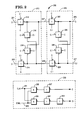
- the flip-flop includes two input terminals 201 and 203, a master section 210, a slave section 220, and two output terminals 205 and 207 and a clock enable circuit 230.
- the master section comprises four CMOS tristate inverters 212, 214, 216 and 2218, hereinafter referred to as TI 212, TI 214, TI 216 and TI 218.
- TI 212 is connected to input terminal 201.
- TI 214 is connected to input terminal 203.
- TI 216 has its input connected to the outputs of TI 214 and TI 218 and its output coupled to the output of TI 212.
- TI 218 has its input connected to the output of TI 212 and TI 216 and its output coupled to the output of TI 214.
- Line 247 which is connected to the outputs of TI 212 and TI 216, forms one output of master section 210, and line 249, which is connected to the outputs of TI 214 and TI 218, forms a second output of the master section.
- Slave section 220 is identical in construction to master section 210.
- the slave section includes CMOS tristate inverter 222, 224, 226 and 228 connected together as follows.
- TI 222 has its input connected to line 247.
- TI 224 has its input connected to line 249.
- TI 226 has its input connected to the outputs of TI 224 and TI 228 and its output connected to the output of TI 222.
- TI 228 has its input connected to the outputs of TI 222 and TI 226 and its output connected to the output of TI 224.
- the outputs of TI 222 and TI 226 are connected to output terminal 205 and the outputs of TI 224 and TI 228 are connected to output terminal 207.
- Each of the tristate inverters described above includes p and n control inputs connected to receive clock and complemented clock signals.
- the n control inputs of TI 212, TI 214, TI 226 and TI 228 and the p control inputs of TI 216, TI 218, TI 222 and TI 224 are connected to receive clock signal C, while the p control inputs of TI 212, TI 214, TI 226 and TI 228 and the n control inputs of TI 216, TI 218, TI 222 and TI 224 are connected to receive complemented clock signal C/.
- Each tristate inverter generates an output signal which is the complement of the signal received at its input when a LOW signal is received at its p control input and a HIGH signal is received at its n control input.
- a clock enable circuit 230 which can be included with the flip-flop circuit to control the generation of signals C and C/.
- the enable circuit comprises NAND gates 235 and 239. Each NAND gate has an input connected to receive an external clock signal CLK and an enable signal ENBL.
- the output of NAND gate 235 is provided to an inverter 237 to generate signal C.
- the output of gate 239 is provided to inverters 241 and 243, connected in series, to generate signal C/.
- the enable signal is held HIGH signals C and C/ are generated, signal C being equal to clock signal CLK and signal C/ being the complement of signal CLK.
- the enable signal is LOW, signal C is held LOW and signal C/ is held HIGH.
- Tristate inverters 212 and 214 are disabled and therefore data presented to the flip-flop on input lines 201 and 203 will not be accepted by the circuit.
- Tristate inverters 216, 218, 222 and 224 are all enabled and operate as described below to maintain output signals Q and Q/ at the last received values of D and D/, respectively.
- tristate inverters 216, 218, 222 and 224 are disabled, producing no output (high impedance state).
- Output signals Q and Q/ are maintained at their values prior to signal C changing state by the operation of enabled tristate inverters 226 and 228.
- TI 226 generates Q/ by inverting Q, while TI 228 simultaneously inverts Q/ to produce Q.
- the HIGH state of clock signal C enables TI 212 and TI 214, which invert input signals D and D/, respectively.
- the inverted D input signal which is equivalent to signal D/, is provided on line 247 to disabled TI 222 and the inverted signal D/, which is equivalent to signal D, is provided on line 249 to disabled TI 224.
- New data is not placed onto the output lines 205 and 207 when clock signal C obtains a HIGH state.
- TI 212 and TI 214 are disabled.
- TI 216 and TI 218 are enabled to maintain the signal states residing on lines 247 and 249 at their values prior to signal C changing to its LOW state.
- TI 222 and TI 224 are enabled to invert the latched values present on lines 247 and 249, respectively, the outputs of these two tristate inverters being the new values for output signals Q and Q/.
- TI 226 and TI 228 are disabled.
- the circuit operation continues as described above with every change of state of clock signal C.
- Data present at input terminals 201 and 203 during a HIGH state of clock signal C will be provided to outputs Q and Q/, respectively, at the change of state of signal C from HIGH to LOW, and latched until the next HIGH to LOW transition.
- incorporation of the enable circuitry into the flip-flop circuit permits additional control over the operation of the flip-flop.
- a LOW state for signal ENBL sets clock signal C to a LOW state, disabling tristate inverters 212, 214, 226 and 228 and enabling tristate inverters 216, 218, 222 and 224.
- the operational states of the tristate inverters are not permitted to change until signal ENBL goes HIGH.
- FIG. 3 is a schematic of a high speed, CMOS D-type flip-flop including an asynchronous reset, according to the present invention.
- the reset feature is provided by substituting clocked NAND gates 316 and 328 for tristate inverters 216 and 228 of Figure 2.
- a reset signal RST/ is provided to one input of each clocked NAND gate via line 301.
- signal RST/ is HIGH
- the operation of the circuit of Figure 3 is the same as that previously described in connection with the circuit of Figure 2.
- signal RST/ is LOW
- output signals Q and Q/ are set LOW and HIGH, respectively.
- Inclusion of clocked NAND gates 318 and 328 into the flip-flop does, however, reduce the operating speed of the circuit.
- circuit design is intended for use in standard cell libraries or gate array libraries.
- the circuit of Figure 2 has been simulated and compared with other standard cell and gate array offerings and shown to be forty percent faster than prior fast flip-flop library offerings.
- the present circuit will operate up to a maximum clock rate of two hundred megahertz under commercial operating conditions.
- the circuit has been designed to minimize the effects of clock skew which come about as a result of the use of external gated clocks. This has been accomplished by the inclusion of a clock enable circuit, as shown in Figures 2 and 3, inside the flip-flop where the skew can be controlled by the cell designer.
Claims (4)
- Getaktete CMOS-Flipflopschaltung des D-Typs umfassend einen ersten, zum Empfangen eines binären Eingangssignals ausgeführten Eingangsanschlußpunkt (201) und einen zweiten, zum Empfangen des Komplements des genannten binären Eingangssignals ausgeführten Eingangsanschlußpunkt (203), einen zum Vorsehen eines binären Ausgangssignals ausgeführten Q-Ausgangsanschlußpunkt (205) und einen zum Vorsehen des Komplements des genannten binären Ausgangssignals ausgeführten Q/-Ausgangsanschlußpunkt (207), einen ersten Datenweg, der ausgeführt ist, um den Zustand des am genannten ersten Eingangsanschlußpunkt (201) empfangenen binären Eingangssignals zum genannten Q-Ausgangsanschlußpunkt (205) vorzusehen, einen zweiten Datenweg, der ausgeführt ist, um den Zustand des am genannten zweiten Eingangsanschlußpunkt (203) empfangenen komplementierten binären Eingangssignals zum genannten Q/-Ausgangsanschlußpunkt (207) vorzusehen, und einen Master-Teil (210) und einen Slave-Teil (220) aufweisend, wobei der genannte Master-Teil (210) auf ein Taktsignal anspricht, um binäre Ausgangssignale zum genannten Slave-Teil (220) vorzusehen, wenn das genannte Taktsignal in einem ersten binären Zustand ist, und um die Zustände der genannten, zuletzt aufgezählten binären Ausgangssignale zu speichern, wenn das genannte Taktsignal in einem zweiten binären Zustand ist, und wobei der genannte Slave-Teil (220) auf das genannte Taktsignal anspricht, um binäre Ausgangssignale zum genannten Q- und Q/-Ausgangsanschlußpunkt (205, 207) vorzusehen, wenn das genannte Taktsignal im genannten zweiten binären Zustand ist, und um die Zustände der genannten, zuletzt aufgezählten binären Ausgangssignale zu speichern, wenn das genannte Taktsignal im genannten ersten binären Zustand ist, dadurch gekennzeichnet, daß der genannte Master-Teil (210) einen ersten (212), zweiten (214), dritten (216) und vierten (218) Dreizustands-Inverter aufweist, wobei der genannte erste Dreizustands-Inverter (212) zum Empfangen des genannten binären Eingangssignals angeschlossen ist, der genannte zweite Dreizustands-Inverter (214) zum Empfangen des genannten zweiten binären Eingangssignals angeschlossen ist, der Eingang des genannten dritten Dreizustands-Inverters (216) am Ausgang des genannten zweiten Dreizustands-Inverters (214) angeschlossen ist und sein Ausgang am Ausgang des genannten ersten Dreizustands-Inverters (212) angeschlossen ist, wobei die vereinigten Ausgänge des genannten ersten und dritten Dreizustands-Inverters (212, 216) einen Ausgang des genannten Master-Teils (210) bilden, und der Eingang des genannten vierten Dreizustands-Inverters (218) am Ausgang des genannten ersten Dreizustands-Inverters (212) angeschlossen ist und sein Ausgang am Ausgang des genannten zweiten Dreizustands-Inverters (214) angeschlossen ist, wobei die vereinigten Ausgänge des genannten zweiten und vierten Inverters (214, 218) einen zweiten Ausgang des genannten Master-Teils (210) bilden; wobei ein Slave-Teil einen fünften (222), sechsten (224), siebten (226) und achten (228) Dreizustands-Inverter aufweist, wobei der genannte fünfte Dreizustands-Inverter (222) zum Empfangen des vereinigten Ausgangs des genannten ersten und dritten Dreizustands-Inverters (212, 216) angeschlossen ist und sein erster Ausgang am genannten Q-Ausgangsanschlußpunkt (205) angeschlossen ist, der genannte sechste Dreizustands-Inverter (224) zum Empfangen des vereinigten Ausgangs des genannten zweiten und vierten Dreizustands-Inverters (214, 218) angeschlossen ist und sein Ausgang am genannten Q/-Ausgangsanschlußpunkt (207) angeschlossen ist, der Eingang des genannten siebten Dreizustands-Inverters (226) an den Ausgang des genannten sechsten Dreizustands-Inverters (224) angeschlossen ist und sein Ausgang an den genannten Q-Ausgangsanschlußpunkt (205) angeschlossen ist, und der Eingang des genannten achten Dreizustands-Inverters (228) am Ausgang des genannten fünften Dreizustands-Inverters (222) angeschlossen ist und sein Ausgang am genannten Q/-Ausgangsanschlußpunkt (207) angeschlossen ist, wobei der genannte erste (212), zweite (214), siebte (226) und achte (228) Dreizustands-Inverter auf das genannte Taktsignal anspricht, um einen Ausgang zu erzeugen, wenn das genannte Taktsignal im genannten ersten binären Zustand ist, und der genannte dritte (216), vierte (218), fünfte (222) und sechste (224) Dreizustands-Inverter auf das genannte Taktsignal anspricht, um einen Ausgang zu erzeugen, wenn das genannte Taktsignal im genannten zweiten binären Zustand ist.
- CMOS-Flipflopschaltung nach Anspruch 1, dadurch gekennzeichnet, daß die genannte Flipflopschaltung eine Taktfreigabeschaltung mit ersten auf ein Freigabesignal (ENBL) ansprechenden Mitteln (235, 237) zum Zulassen der Übertragung des genannten Taktsignals, wenn das genannte Freigabesignal (ENBL) in einem ersten binären Zustand ist, und zum Verhindern der Übertragung des genannten Taktsignals, wenn das genannte Freigabesignal (ENBL) in einem zweiten binären Zustand ist, und zweiten Mitteln (239, 241, 243) zum Erzeugen des Komplements des Ausgangs der genannten ersten Mittel aufweist.
- CMOS-Flipflopschaltung nach Anspruch 2, dadurch gekennzeichnet, daß das genannte erste Mittel ein NAND-Glied (235), das zum Empfangen des genannten Taktsignals und des genannten Freigabesignals (ENBL) ausgeführt ist, und einen ersten Inverter (237) aufweist, der zum Empfangen des Ausgangs des genannten NAND-Glieds (235) ausgeführt ist, und das genannte zweite Mittel ein zweites NAND-Glied (239), das zum Empfangen des genannten Taktsignals und des genannten Freigabesignals (ENBL) ausgeführt ist, einen zweiten Inverter (241), der zum Empfangen des Ausgangs des genannten zweiten NAND-Glieds (239) ausgeführt ist, und eine dritten Inverter (243) aufweist, der zum Empfangen des Ausgangs des genannten zweiten Inverters (241) ausgeführt ist.
- CMOS-Flipflopschaltung nach Anspruch 1, 2 oder 3, dadurch gekennzeichnet, daß der genannte dritte und achte Dreizustands-Inverter durch ein erstes beziehungsweise ein zweites getaktetes NAND-Glied (316, 328) ersetzt wird, das zum Empfangen eines gemeinsamen Rücksetzsignals für die genannte Flipflopschaltung (200) ausgeführt ist.
Applications Claiming Priority (2)
| Application Number | Priority Date | Filing Date | Title |
|---|---|---|---|
| US07/572,596 US5140180A (en) | 1990-08-24 | 1990-08-24 | High speed cmos flip-flop employing clocked tristate inverters |
| US572596 | 1990-08-24 |
Publications (3)
| Publication Number | Publication Date |
|---|---|
| EP0472426A2 EP0472426A2 (de) | 1992-02-26 |
| EP0472426A3 EP0472426A3 (en) | 1992-05-13 |
| EP0472426B1 true EP0472426B1 (de) | 1996-11-13 |
Family
ID=24288543
Family Applications (1)
| Application Number | Title | Priority Date | Filing Date |
|---|---|---|---|
| EP91307713A Expired - Lifetime EP0472426B1 (de) | 1990-08-24 | 1991-08-21 | CMOS-Flipflop-Schaltung |
Country Status (4)
| Country | Link |
|---|---|
| US (1) | US5140180A (de) |
| EP (1) | EP0472426B1 (de) |
| JP (1) | JP3299290B2 (de) |
| DE (1) | DE69123100T2 (de) |
Families Citing this family (10)
| Publication number | Priority date | Publication date | Assignee | Title |
|---|---|---|---|---|
| FR2692072A1 (fr) * | 1992-06-05 | 1993-12-10 | Sgs Thomson Microelectronics | Bascule bistable à commande de réinitialisation. |
| DE69514918T2 (de) * | 1995-08-31 | 2000-06-15 | St Microelectronics Srl | D-Flip-Flop mit asynchronem Laden von Daten |
| US5999029A (en) * | 1996-06-28 | 1999-12-07 | Lsi Logic Corporation | Meta-hardened flip-flop |
| FR2756120B1 (fr) * | 1996-11-19 | 1999-02-05 | Sgs Thomson Microelectronics | Dispositif de conversion serie/parallele d'un signal haute frequence de faible amplitude |
| US6633188B1 (en) * | 1999-02-12 | 2003-10-14 | Texas Instruments Incorporated | Sense amplifier-based flip-flop with asynchronous set and reset |
| GB2361121A (en) * | 2000-04-04 | 2001-10-10 | Sharp Kk | A CMOS LCD scan pulse generating chain comprising static latches |
| GB0013790D0 (en) | 2000-06-06 | 2000-07-26 | Texas Instruments Ltd | Improvements in or relating to flip-flop design |
| US7098833B2 (en) * | 2004-06-04 | 2006-08-29 | Texas Instruments Incorporated | Tri-value decoder circuit and method |
| US9876501B2 (en) | 2013-05-21 | 2018-01-23 | Mediatek Inc. | Switching power amplifier and method for controlling the switching power amplifier |
| WO2022256633A1 (en) * | 2021-06-03 | 2022-12-08 | Synopsys, Inc. | D-type wholly dissimilar high-speed static set-reset flip flop |
Family Cites Families (13)
| Publication number | Priority date | Publication date | Assignee | Title |
|---|---|---|---|---|
| US4463440A (en) * | 1980-04-15 | 1984-07-31 | Sharp Kabushiki Kaisha | System clock generator in integrated circuit |
| US4506167A (en) * | 1982-05-26 | 1985-03-19 | Motorola, Inc. | High speed logic flip-flop latching arrangements including input and feedback pairs of transmission gates |
| JPS59134918A (ja) * | 1983-01-24 | 1984-08-02 | Toshiba Corp | ラツチ回路 |
| US4628217A (en) * | 1984-03-22 | 1986-12-09 | Sperry Corporation | Fast scan/set testable latch using two levels of series gating with one current source |
| US4691122A (en) * | 1985-03-29 | 1987-09-01 | Advanced Micro Devices, Inc. | CMOS D-type flip-flop circuits |
| US4785204A (en) * | 1985-06-21 | 1988-11-15 | Mitsubishi Denki Kabushiki Kaisha | Coincidence element and a data transmission path |
| JPS6295016A (ja) * | 1985-10-21 | 1987-05-01 | Mitsubishi Electric Corp | ラツチ回路 |
| US4777388A (en) * | 1986-04-24 | 1988-10-11 | Tektronix, Inc. | Fast latching flip-flop |
| EP0270296A3 (de) * | 1986-12-01 | 1990-02-07 | Fujitsu Limited | Halbleiter-Logikschaltung |
| JPH077901B2 (ja) * | 1988-02-29 | 1995-01-30 | 沖電気工業株式会社 | フリップフロップ回路 |
| US4932002A (en) * | 1988-09-30 | 1990-06-05 | Texas Instruments, Incorporated | Bit line latch sense amp |
| US5036217A (en) * | 1989-06-02 | 1991-07-30 | Motorola, Inc. | High-speed low-power flip-flop |
| US5017815A (en) * | 1989-12-20 | 1991-05-21 | At&T Bell Laboratories | Sense amplifier with selective pull up |
-
1990
- 1990-08-24 US US07/572,596 patent/US5140180A/en not_active Expired - Lifetime
-
1991
- 1991-08-21 EP EP91307713A patent/EP0472426B1/de not_active Expired - Lifetime
- 1991-08-21 DE DE69123100T patent/DE69123100T2/de not_active Expired - Lifetime
- 1991-08-22 JP JP23374291A patent/JP3299290B2/ja not_active Expired - Lifetime
Also Published As
| Publication number | Publication date |
|---|---|
| JPH04271512A (ja) | 1992-09-28 |
| US5140180A (en) | 1992-08-18 |
| EP0472426A2 (de) | 1992-02-26 |
| DE69123100D1 (de) | 1996-12-19 |
| EP0472426A3 (en) | 1992-05-13 |
| JP3299290B2 (ja) | 2002-07-08 |
| DE69123100T2 (de) | 1997-06-12 |
Similar Documents
| Publication | Publication Date | Title |
|---|---|---|
| KR940005003B1 (ko) | 재순환 능력을 가진 에지 트리거형 d형 플립플롭 주사래치 셀 | |
| JP3587248B2 (ja) | スキャン用フリップフロップ | |
| US5623223A (en) | Glitchless clock switching circuit | |
| US6853215B1 (en) | Programmable I/O element circuit for high speed logic devices | |
| US4558236A (en) | Universal logic circuit | |
| US5656962A (en) | Master-slave flip-flop circuit with bypass | |
| US6566927B2 (en) | Complementary pass transistor based flip-flop | |
| US6753714B2 (en) | Reducing power and area consumption of gated clock enabled flip flops | |
| US5041742A (en) | Structured scan path circuit for incorporating domino logic | |
| US5933038A (en) | Flip-flop with logic function incorporated therein with minimal time penalty | |
| US5302866A (en) | Input circuit block and method for PLDs with register clock enable selection | |
| US8030969B2 (en) | Semiconductor integrated circuit | |
| EP0472426B1 (de) | CMOS-Flipflop-Schaltung | |
| US5426380A (en) | High speed processing flip-flop | |
| US4506167A (en) | High speed logic flip-flop latching arrangements including input and feedback pairs of transmission gates | |
| US6069495A (en) | High-speed logic embodied differential dynamic CMOS true single phase clock latches and flip-flops with single transistor clock latches | |
| US5293079A (en) | Formatter circuit | |
| WO2023143632A1 (zh) | 基于数据比较进行时钟门控的触发单元 | |
| KR20180129617A (ko) | 순차 회로에서 스캔 홀드-타임 위반 및 저전압 동작을 개선하기 위한 시스템 및 방법 | |
| US5047658A (en) | High frequency asynchronous data synchronizer | |
| US5742190A (en) | Method and apparatus for clocking latches in a system having both pulse latches and two-phase latches | |
| US5638008A (en) | Method and apparatus for generating an asynchronously clocked signal in a synchronously clocked programmable device | |
| EP0496171B1 (de) | Bistabile integrierte Halbleiterschaltung | |
| WO1997007592A1 (en) | Mos master-slave flip-flop with reduced number of pass gates | |
| EP0085489B1 (de) | Schaltung einer Speicher enthaltende Logikanordnung |
Legal Events
| Date | Code | Title | Description |
|---|---|---|---|
| PUAI | Public reference made under article 153(3) epc to a published international application that has entered the european phase |
Free format text: ORIGINAL CODE: 0009012 |
|
| AK | Designated contracting states |
Kind code of ref document: A2 Designated state(s): DE GB |
|
| PUAL | Search report despatched |
Free format text: ORIGINAL CODE: 0009013 |
|
| AK | Designated contracting states |
Kind code of ref document: A3 Designated state(s): DE GB |
|
| 17P | Request for examination filed |
Effective date: 19921026 |
|
| RAP1 | Party data changed (applicant data changed or rights of an application transferred) |
Owner name: NCR INTERNATIONAL INC. |
|
| RAP1 | Party data changed (applicant data changed or rights of an application transferred) |
Owner name: AT&T GLOBAL INFORMATION SOLUTIONS INTERNATIONAL IN |
|
| RAP1 | Party data changed (applicant data changed or rights of an application transferred) |
Owner name: AT&T GLOBAL INFORMATION SOLUTIONS INTERNATIONAL IN Owner name: HYUNDAI ELECTRONICS AMERICA |
|
| 17Q | First examination report despatched |
Effective date: 19950714 |
|
| GRAG | Despatch of communication of intention to grant |
Free format text: ORIGINAL CODE: EPIDOS AGRA |
|
| GRAH | Despatch of communication of intention to grant a patent |
Free format text: ORIGINAL CODE: EPIDOS IGRA |
|
| GRAH | Despatch of communication of intention to grant a patent |
Free format text: ORIGINAL CODE: EPIDOS IGRA |
|
| RAP1 | Party data changed (applicant data changed or rights of an application transferred) |
Owner name: HYUNDAI ELECTRONICS AMERICA Owner name: AT&T GLOBAL INFORMATION SOLUTIONS INTERNATIONAL IN Owner name: SYMBIOS LOGIC INC. |
|
| GRAA | (expected) grant |
Free format text: ORIGINAL CODE: 0009210 |
|
| AK | Designated contracting states |
Kind code of ref document: B1 Designated state(s): DE GB |
|
| REF | Corresponds to: |
Ref document number: 69123100 Country of ref document: DE Date of ref document: 19961219 |
|
| RAP2 | Party data changed (patent owner data changed or rights of a patent transferred) |
Owner name: SYMBIOS LOGIC INC. Owner name: NCR INTERNATIONAL, INC. Owner name: HYUNDAI ELECTRONICS AMERICA |
|
| PLBE | No opposition filed within time limit |
Free format text: ORIGINAL CODE: 0009261 |
|
| STAA | Information on the status of an ep patent application or granted ep patent |
Free format text: STATUS: NO OPPOSITION FILED WITHIN TIME LIMIT |
|
| 26N | No opposition filed | ||
| REG | Reference to a national code |
Ref country code: GB Ref legal event code: IF02 |
|
| REG | Reference to a national code |
Ref country code: GB Ref legal event code: 732E |
|
| REG | Reference to a national code |
Ref country code: GB Ref legal event code: 732E |
|
| REG | Reference to a national code |
Ref country code: GB Ref legal event code: 732E |
|
| PGFP | Annual fee paid to national office [announced via postgrant information from national office to epo] |
Ref country code: DE Payment date: 20100827 Year of fee payment: 20 |
|
| PGFP | Annual fee paid to national office [announced via postgrant information from national office to epo] |
Ref country code: GB Payment date: 20100825 Year of fee payment: 20 |
|
| REG | Reference to a national code |
Ref country code: DE Ref legal event code: R071 Ref document number: 69123100 Country of ref document: DE |
|
| REG | Reference to a national code |
Ref country code: DE Ref legal event code: R071 Ref document number: 69123100 Country of ref document: DE |
|
| PG25 | Lapsed in a contracting state [announced via postgrant information from national office to epo] |
Ref country code: GB Free format text: LAPSE BECAUSE OF EXPIRATION OF PROTECTION Effective date: 20110820 |
|
| PG25 | Lapsed in a contracting state [announced via postgrant information from national office to epo] |
Ref country code: DE Free format text: LAPSE BECAUSE OF EXPIRATION OF PROTECTION Effective date: 20110822 |