EP0472285A2 - Externspeicherzugriffssteuerung für eine Verarbeitungsanlage - Google Patents
Externspeicherzugriffssteuerung für eine Verarbeitungsanlage Download PDFInfo
- Publication number
- EP0472285A2 EP0472285A2 EP91306492A EP91306492A EP0472285A2 EP 0472285 A2 EP0472285 A2 EP 0472285A2 EP 91306492 A EP91306492 A EP 91306492A EP 91306492 A EP91306492 A EP 91306492A EP 0472285 A2 EP0472285 A2 EP 0472285A2
- Authority
- EP
- European Patent Office
- Prior art keywords
- external memory
- external
- memory
- control system
- enable
- Prior art date
- Legal status (The legal status is an assumption and is not a legal conclusion. Google has not performed a legal analysis and makes no representation as to the accuracy of the status listed.)
- Granted
Links
Images

Classifications
-
- G—PHYSICS
- G06—COMPUTING OR CALCULATING; COUNTING
- G06F—ELECTRIC DIGITAL DATA PROCESSING
- G06F1/00—Details not covered by groups G06F3/00 - G06F13/00 and G06F21/00
- G06F1/26—Power supply means, e.g. regulation thereof
- G06F1/32—Means for saving power
- G06F1/3203—Power management, i.e. event-based initiation of a power-saving mode
- G06F1/3206—Monitoring of events, devices or parameters that trigger a change in power modality
- G06F1/3215—Monitoring of peripheral devices
-
- G—PHYSICS
- G06—COMPUTING OR CALCULATING; COUNTING
- G06F—ELECTRIC DIGITAL DATA PROCESSING
- G06F1/00—Details not covered by groups G06F3/00 - G06F13/00 and G06F21/00
- G06F1/04—Generating or distributing clock signals or signals derived directly therefrom
-
- G—PHYSICS
- G06—COMPUTING OR CALCULATING; COUNTING
- G06F—ELECTRIC DIGITAL DATA PROCESSING
- G06F1/00—Details not covered by groups G06F3/00 - G06F13/00 and G06F21/00
- G06F1/26—Power supply means, e.g. regulation thereof
- G06F1/32—Means for saving power
- G06F1/3203—Power management, i.e. event-based initiation of a power-saving mode
- G06F1/3234—Power saving characterised by the action undertaken
- G06F1/325—Power saving in peripheral device
- G06F1/3275—Power saving in memory, e.g. RAM, cache
-
- Y—GENERAL TAGGING OF NEW TECHNOLOGICAL DEVELOPMENTS; GENERAL TAGGING OF CROSS-SECTIONAL TECHNOLOGIES SPANNING OVER SEVERAL SECTIONS OF THE IPC; TECHNICAL SUBJECTS COVERED BY FORMER USPC CROSS-REFERENCE ART COLLECTIONS [XRACs] AND DIGESTS
- Y02—TECHNOLOGIES OR APPLICATIONS FOR MITIGATION OR ADAPTATION AGAINST CLIMATE CHANGE
- Y02D—CLIMATE CHANGE MITIGATION TECHNOLOGIES IN INFORMATION AND COMMUNICATION TECHNOLOGIES [ICT], I.E. INFORMATION AND COMMUNICATION TECHNOLOGIES AIMING AT THE REDUCTION OF THEIR OWN ENERGY USE
- Y02D10/00—Energy efficient computing, e.g. low power processors, power management or thermal management
Definitions
- the present invention generally relates to processing systems and more particularly to processing systems wherein external memory accessing is required.
- the present invention still more particularly relates to an external memory access control for a processing system which reduces power consumption of the processing system by establishing external memory enable time durations which are independent from the external memory accessing rate.
- Processing systems which include at least one microprocessor are well known in the art.
- the microprocessor is generally required to access external memory for data and/or instructions. It is also common for microprocessor-based processing systems to have periods of high activity, wherein a large number of operations are performed per unit of time, interspersed with periods of low activity, wherein relatively few operations are performed per unit of time.
- the external memory access rate of the microprocessor To reduce the power consumption of such processing systems during periods of low activity, it has been common in the prior art to reduce the external memory access rate of the microprocessor. This is typically accomplished through the use of either a variable-rate oscillator clock source or by incorporating into the microprocessor a clock divider circuit to reduce the external memory access rate. Since the microprocessor communicates with external memory through a bus, the external memory access rate may also be referred to as a bus access rate.
- RAM random access memory
- EPROM electrically programmable read only memory
- the CHIP ENABLE signal for external RAM and/or EPROM is decoded either within the microprocessor or by logic external to the micro- processor from bus control signals provided by the microprocessor.
- Typical bus control signals as for example with respect to the 8031 class of microcontroller include the address lines, ALE, PSEN * , RD * , and WR * .
- the names and functions of the bus control signals differ from one microprocessor/microcontroller to another, but the fundamental concept of providing enabling and directional information to devices external to the microprocessor remains the same.
- the limitation in the prior art with respect to low-power processing system operation is that when the memory access rate of existing microprocessors and controllers is reduced in an attempt to save system power, the width of the bus control signals provided by the microprocessor (the external memory enable time durations) varies in direct proportion to the bus rate (external memory access rate) of the processor. As a result, even though the external memory access rate of the processor is reduced, the external memory enable time durations proportionately increase. Hence, the slower the memory access rate becomes, the longer the external memory enable time durations become. This is wasteful of system power since the external memory devices are enabled for a much longer time duration then is required to complete the accessing of the external memory devices.
- the external memory access control system includes clock means for providing a clock signal for determining the number of external memory accesses per unit of time and enable duration control means coupled to the clock means and being arranged to provide the external memory with external memory enable time duration control signals for establishing external memory enable time durations which are independent from the number of external memory accesses per unit of time.
- the memory access control system includes clock means for providing memory access rates including a maximum rate and a slow rate and memory enable duration control means having an input coupled to the clock means and an output coupled to the memory for providing the memory with enable signals having a fixed duration corresponding to the maximum access rate regardless of the memory access rate provided by the clock means.
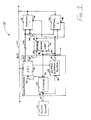
- the processing system 10 generally includes a clock source 12, a microprocessor 14, address decode logic 16, a first memory 18, a second memory 20, and a bus 22.
- the clock source 12, address decode logic 16, the first memory 18, and the second memory 20, are all external to the microprocessor 14.
- the clock source 12, the microprocessor 14, address decode logic 16, the first memory 18 and the second memory 20 may all be implemented in integrated circuit form with each being contained within separate integrated circuit devices.
- the microprocessor 14 includes a divider circuit 24, a central processing unit 26, and an enable duration control 28, in accordance with the present invention.
- the divider circuit 24 has an input 30 coupled to the output 32 of the clock source 12 for receiving the clock output of the clock source 12.
- the divider 24 also has an output 34 which is coupled to a clock input 36 of the central processing unit 26 and a clock input 38 of the address decode logic.
- the clock source 12 provides a clock output comprising a relatively high frequency pulse train which is divided by the divider circuit 24 to provide at its output 34 timing and synchronizing clock signals for the processing system.
- the output frequency of the clock signal provided by the divider 24 at its output 34 determines the external memory access rate by the microprocessor 14.
- the enable duration control 28 includes an input 40 which is coupled between the output 32 of the clock source 12 and the input 30 of the divider circuit 24.
- the enable duration control provides at its output 42 external memory enable time duration signals which determine the time in which the external memories are enabled for utilizing the bus during each access of the external memories by the microprocessor 14.
- the enable time durations established by the enable duration control 28 are independent from the external memory access rate determined by the divider 24.
- the enable duration control 28 also includes an input 41 coupled to the central processing unit 26. This input allows the central processing unit 26 to control when the enable time durations established by the enable duration control begin, but synchronized to the clock source output.
- the output 42 of the enable duration control 28 comprises a plurality of lines denoted by the hash mark, which lines are coupled to bus enable control inputs 44 of the address decode logic 16, the bus enable inputs 46 of the first external memory 18, and the bus enable inputs 48 of the second external memory 50.
- the output 42 of the enable duration control 28 may be coupled to the address decode logic and external memories as illustrated in Figure 1, may be coupled directly and only to the external memories 18 and 20, or may be coupled to the external memories 18 and 20 only through the address decode logic depending upon the particular processing system design and without departing from the present invention.
- the central processing unit 26 includes a first output 50 for providing a first set of external memory addresses to the address decode logic 16 over a first plurality of lines 52.
- the central processing unit 26 also includes a second output 54 for providing a second set of external memory addresses to the external memories 18 and 20 over a second plurality of output lines 56.
- the address decode logic includes an output 58 which is coupled to the first and second memories 18 and 20 over a plurality of output lines 60 for conveying to the external memories 18 and 20 external memory or chip select signals.
- the second set of addresses provided by the central processing unit 26 are utilized for selecting the desired memory location within the external memory to be accessed.
- Each of the memories 18 and 20 preferably includes a plurality of memory locations with each memory location having a unique address with respect to its memory.
- the memory address locations of the external memories may have duplicated addresses.
- the chip select signals provided by the address decode logic 16 over lines 60 select the memory to be accessed and the second set of memory addresses conveyed over lines 56 select the particular memory location to be accessed within the selected external memory to be accessed.
- the central processing unit 26 is coupled to the bus 22 and the external memories 18 and 20 are also coupled to the bus 22.
- the central processing unit 26 and external memories 18 and 20 are coupled to the bus 22 to enable the microprocessor 14 to communicate with the external memories to permit the central processing unit to read data and/or instructions from the external memories or to write data into the external memories during external memory accesses.
- the clock source 12 provides at its output 32 a clock output in the form of a relatively high frequency pulse train from which the external memory access rate is derived.
- the external memory access rate is derived from the output 34 of the divider 24.
- the frequency of the clock source defines the maximum access rate of the external memories by the microprocessor.
- the divider 24 will divide the clock rate of the clock output provided by the clock source 12 by a factor of one.
- the access rate is reduced to conserve power and the divider will then divide the clock rate of the clock output provided by the clock source 12 by a factor of thirty-two, for example, in accordance with this preferred embodiment.
- the clock signal provided at the output 34 of the divider 24 thus determines the external memory access rate of the microprocessor and is also used for other timing and synchronizing purposes within the processing system 10.
- the enable duration control 28 establishes the time duration in which the external memories are enabled during each external memory access and is also responsive to the central processing unit 26 for beginning the memory enable time durations at the proper time.
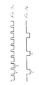
- Figure 3a represents the enable duration control signal provided to the external memories 18 and 20 during periods of high microprocessor activity.
- the enable control signal is applied to the bus enable inputs 46 and 48 of the external memories 18 and 20 respectively.
- the external memory bus enable inputs 46 and 48 are rendered active to turn on the external memories 18 and 20 respectively. Because the enable duration control is coupled between the clock source 12 and the divider 24, enable time durations correspond to the maximum external memory rate of the microprocessor 14.
- the central processing unit 26 At the beginning of each external memory access, the central processing unit 26 generates the first and second sets of external memory addresses at outputs 50 and 54 respectively, the first set of external memory addresses being decoded by the address decode logic 16 for selecting the particular external memory to be accessed, and the second set of external memory addresses being applied directly to the external memories 18 and 20 for selecting the particular memory location to be accessed in the external memory to be accessed.
- the external memory select signals, the memory location address signals, and the enable duration control signals are applied to the external memories 18 and 20, the particular external memory 18 or 20 being accessed is then turned on and enabled to use the bus.
- the enable duration control 28 will apply a read enable duration control signal to the bus enable inputs 46 and 48 of external memories 18 and 20.
- the enable duration control signal in accordance with this preferred embodiment, is also applied to the address decode logic but, without departing from the present invention, could be applied to the external memories only through the address decode logic, or be applied directly to the external memories without being applied to the address decode logic.
- the enable duration control 28 will apply a write enable duration control signal to the bus enable inputs 46 and 48 of the external memories 18 and 20 respectively. In either case, the read or write enable duration control signal will take the form of the waveform illustrated in Figure 3a. As long as the enable duration control signal is at a low level during time periods Ti, the accessed external memory will be turned on and enabled.
- Figure 3b represents the enable duration control signal for periods of low microprocessor activity. During such periods, the external memories need not be accessed at the maximum rate and, in order to conserve power, the external memory access rate is shown in Figure 3b for illustrative purposes only to be reduced by a factor of 1/3, although in actual practice, as previously described, an access rate reduction of 1/32 would be preferable.
- the external memory access rate is determined by the divider 24 dividing the clock output of the clock source 12 by a factor of 3.
- the enable time durations of the external memories is based upon the external memory access rate and hence, upon the output of the divider 24.
- the external enable time durations are proportional to the dividing factor of the divider.
- the external memory enable time durations during each external memory access at the slower rate will be three times as long as the external memory enable time durations during each external memory access at the maximum rate. This represents a waste of power since the shorter external memory enable time duration corresponding to the maximum external memory access rate is adequate for the complete information transfer between the central processing unit and the external memories and thus, completion of an external memory access.
- the enable duration control 28 is coupled between the clock source 12 and the divider 24, it establishes the external memory enable time durations independently from the external memory access rates. As can be seen in Figure 3b, although the external memory access rate is reduced by a factor of three, the external memory enable time durations remain the same for each memory access for the time period of T 1 which corresponds to the external memory enable time duration for the maximum external memory access rate.
- the enable duration control 28 establishes external memory enable time durations for each memory access which remain the same regardless of the external memory access rate. As a result, power is not wasted by allowing the external memories to be on longer than necessary during each memory access while also allowing the external memory access rate to be reduced during periods of low microprocessor activity.
- the enable time duration control 28 may be implemented through the use of logic circuits of the type well known in the art which can establish a fixed external memory address time duration based upon the clock source output or may be, for example, a one-shot multivibrator. The provision of such circuits is well known in the art and need not be described in detail herein.
- FIG 2 it illustrates another processing system 70 embodying the present invention.
- the processing system 70 is essentially identical to the processing system 10 of Figure 1 except that the address decode logic 16 is contained within the microprocessor and is thus integrated with the microprocessor on the same integrated circuit chip.
- the microprocessor 14 of the processing system 70 provides the external memory select signals directly for direct connection to the external memories 18 and 20 without the need for an external address decode logic for decoding the first set of external memory addresses into external memory select signals.
- the processing system 70 functions in the same manner as the processing system 10 previously described.
- an external memory access control for use in a processing system which not only enables the external memory access rates to be reduced during periods of low microprocessor activity to thus reduce power consumption of the processing system, but in addition, also shortens the external memory enable time durations during each memory access during those periods when the external memory access rate is reduced. This further contributes to reduce the power consumption of the processing system which may be exceedingly important when such processing systems are powered by depletable power sources such as battery power sources.
- the external memory enable time durations are remained constant, corresponding to the enable time durations for the maximum external memory access rate, regardless of the external memory access rate of the microprocessor.
Landscapes
- Engineering & Computer Science (AREA)
- Theoretical Computer Science (AREA)
- Physics & Mathematics (AREA)
- General Engineering & Computer Science (AREA)
- General Physics & Mathematics (AREA)
- Memory System (AREA)
- Debugging And Monitoring (AREA)
- Power Sources (AREA)
- Vehicle Body Suspensions (AREA)
- Microcomputers (AREA)
Applications Claiming Priority (2)
| Application Number | Priority Date | Filing Date | Title |
|---|---|---|---|
| US56993590A | 1990-08-20 | 1990-08-20 | |
| US569935 | 1990-08-20 |
Publications (3)
| Publication Number | Publication Date |
|---|---|
| EP0472285A2 true EP0472285A2 (de) | 1992-02-26 |
| EP0472285A3 EP0472285A3 (en) | 1993-01-13 |
| EP0472285B1 EP0472285B1 (de) | 1997-10-08 |
Family
ID=24277524
Family Applications (1)
| Application Number | Title | Priority Date | Filing Date |
|---|---|---|---|
| EP91306492A Expired - Lifetime EP0472285B1 (de) | 1990-08-20 | 1991-07-17 | Speicherzugriffssteuerung |
Country Status (5)
| Country | Link |
|---|---|
| US (1) | US5481690A (de) |
| EP (1) | EP0472285B1 (de) |
| JP (1) | JP3250821B2 (de) |
| AT (1) | ATE159107T1 (de) |
| DE (1) | DE69127873T2 (de) |
Cited By (1)
| Publication number | Priority date | Publication date | Assignee | Title |
|---|---|---|---|---|
| EP0580338A1 (de) * | 1992-07-21 | 1994-01-26 | Advanced Micro Devices, Inc. | Externspeicherzugriffssteuerung für eine Verarbeitungsanlage |
Families Citing this family (9)
| Publication number | Priority date | Publication date | Assignee | Title |
|---|---|---|---|---|
| EP0507427B1 (de) * | 1991-03-01 | 1999-05-06 | Advanced Micro Devices, Inc. | Mikroprozessor mit externem Speicher |
| GB2315347B (en) * | 1993-08-23 | 1998-04-01 | Advanced Risc Mach Ltd | Testing integrated circuits |
| US7114086B2 (en) * | 2002-01-04 | 2006-09-26 | Ati Technologies, Inc. | System for reduced power consumption by monitoring instruction buffer and method thereof |
| EP1742143B1 (de) * | 2005-07-06 | 2018-11-21 | STMicroelectronics Srl | Verfahren und System zur Leistungsverbrauchssteuerung, und entsprechendes Computerprogrammprodukt |
| EP2117244A4 (de) | 2007-02-08 | 2015-04-29 | Ntt Docomo Inc | Funkkommunikationssystem mit einer am wenigsten signifikanten station und einer zwischenstation |
| EP2111053A4 (de) | 2007-02-08 | 2014-08-06 | Ntt Docomo Inc | Funkkommunikationssystem mit einer am wenigsten signifikanten station und einer am meisten signifikanten station |
| US8862924B2 (en) | 2011-11-15 | 2014-10-14 | Advanced Micro Devices, Inc. | Processor with power control via instruction issuance |
| US8503264B1 (en) * | 2011-11-18 | 2013-08-06 | Xilinx, Inc. | Reducing power consumption in a segmented memory |
| US8743653B1 (en) | 2012-06-20 | 2014-06-03 | Xilinx, Inc. | Reducing dynamic power consumption of a memory circuit |
Family Cites Families (18)
| Publication number | Priority date | Publication date | Assignee | Title |
|---|---|---|---|---|
| US3919695A (en) * | 1973-12-26 | 1975-11-11 | Ibm | Asynchronous clocking apparatus |
| JPS5734245A (en) * | 1980-08-09 | 1982-02-24 | Shigeru Toyoshima | Operation processing device |
| JPS5775335A (en) * | 1980-10-27 | 1982-05-11 | Hitachi Ltd | Data processor |
| US4379265A (en) * | 1981-05-26 | 1983-04-05 | Burroughs Corporation | Dual clocking time delay generation circuit |
| US4532587A (en) * | 1981-08-26 | 1985-07-30 | Texas Instruments Incorporated | Single chip processor connected to an external memory chip |
| US4507732A (en) * | 1981-10-05 | 1985-03-26 | Burroughs Corporation | I/O subsystem using slow devices |
| US4685087A (en) * | 1983-08-31 | 1987-08-04 | Texas Instruments Incorporated | SRAM with constant pulse width |
| US4631659A (en) * | 1984-03-08 | 1986-12-23 | Texas Instruments Incorporated | Memory interface with automatic delay state |
| US4617624A (en) * | 1984-04-16 | 1986-10-14 | Goodman James B | Multiple configuration memory circuit |
| US4845632A (en) * | 1985-10-16 | 1989-07-04 | Pitney Bowes Inc. | Electonic postage meter system having arrangement for rapid storage of critical postage accounting data in plural nonvolatile memories |
| US4835728A (en) * | 1986-08-13 | 1989-05-30 | Amdahl Corporation | Deterministic clock control apparatus for a data processing system |
| US5125088A (en) * | 1986-09-08 | 1992-06-23 | Compaq Computer Corporation | Computer system speed control at continuous processor speed |
| US4805137A (en) * | 1987-01-08 | 1989-02-14 | United Technologies Corporation | Bus controller command block processing system |
| US4884234A (en) * | 1987-06-29 | 1989-11-28 | Ncr Corporation | Dynamic RAM refresh circuit with DMA access |
| US4908748A (en) * | 1987-07-28 | 1990-03-13 | Texas Instruments Incorporated | Data processing device with parallel circular addressing hardware |
| US5155812A (en) * | 1989-05-04 | 1992-10-13 | Texas Instruments Incorporated | Devices and method for generating and using systems, software waitstates on address boundaries in data processing |
| US5142684A (en) * | 1989-06-23 | 1992-08-25 | Hand Held Products, Inc. | Power conservation in microprocessor controlled devices |
| DE4029598A1 (de) * | 1990-09-19 | 1992-03-26 | Philips Patentverwaltung | Schaltungsanordnung zur zeitweisen verzoegerung des programmablaufs in einem mikroprozessor |
-
1991
- 1991-07-17 DE DE69127873T patent/DE69127873T2/de not_active Expired - Fee Related
- 1991-07-17 EP EP91306492A patent/EP0472285B1/de not_active Expired - Lifetime
- 1991-07-17 AT AT91306492T patent/ATE159107T1/de not_active IP Right Cessation
- 1991-08-12 JP JP20177091A patent/JP3250821B2/ja not_active Expired - Fee Related
-
1993
- 1993-10-04 US US08/140,820 patent/US5481690A/en not_active Expired - Lifetime
Cited By (2)
| Publication number | Priority date | Publication date | Assignee | Title |
|---|---|---|---|---|
| EP0580338A1 (de) * | 1992-07-21 | 1994-01-26 | Advanced Micro Devices, Inc. | Externspeicherzugriffssteuerung für eine Verarbeitungsanlage |
| US5408639A (en) * | 1992-07-21 | 1995-04-18 | Advanced Micro Devices | External memory access control for a processing system |
Also Published As
| Publication number | Publication date |
|---|---|
| DE69127873D1 (de) | 1997-11-13 |
| EP0472285A3 (en) | 1993-01-13 |
| ATE159107T1 (de) | 1997-10-15 |
| JPH04255043A (ja) | 1992-09-10 |
| DE69127873T2 (de) | 1998-04-16 |
| EP0472285B1 (de) | 1997-10-08 |
| US5481690A (en) | 1996-01-02 |
| JP3250821B2 (ja) | 2002-01-28 |
Similar Documents
| Publication | Publication Date | Title |
|---|---|---|
| US7100061B2 (en) | Adaptive power control | |
| KR100329344B1 (ko) | 전원관리장치및방법 | |
| EP0580338B1 (de) | Externspeicherzugriffssteuerung für eine Verarbeitungsanlage | |
| US5041962A (en) | Computer system with means for regulating effective processing rates | |
| MY116707A (en) | Coprocessor data access control | |
| US5481690A (en) | Power-efficient external memory access control using external memory enable time durations independent of external memory accessing rate | |
| US5845139A (en) | System for providing a host computer with access to a memory on a PCMCIA card in a power down mode | |
| JP2636691B2 (ja) | マイクロコンピュータ | |
| US5606680A (en) | Realtime clock with page mode addressing | |
| EP0208287B1 (de) | Direktspeicherzugriffsteuerungsgerät | |
| US6505304B1 (en) | Timer apparatus which can simultaneously control a plurality of timers | |
| EP0783148A2 (de) | Taktsystem zum Energiesparen | |
| JPH09311812A (ja) | マイクロコンピュータ | |
| GB2304427A (en) | Dynamic clock rate control | |
| JP2730240B2 (ja) | マイクロコンピュータ・システム | |
| JPS6375913A (ja) | パ−ソナルコンピユ−タ用電力制御装置 | |
| US20020133677A1 (en) | Digital data processing system | |
| JPH0542525Y2 (de) | ||
| KR970002410B1 (ko) | 컴퓨터시스템에 있어서 중앙제어기와 주변기기간의 인터페이스장치 | |
| JP2570837B2 (ja) | マイクロプロセッサ | |
| JPH0460598A (ja) | Pcm音源システム | |
| JPH08273355A (ja) | パワーダウンメモリ制御ユニット | |
| JPS61241851A (ja) | 読出し回路 | |
| JPH07295675A (ja) | Cpuシステムの省電力化方式 | |
| US20040210730A1 (en) | Dram control circuit |
Legal Events
| Date | Code | Title | Description |
|---|---|---|---|
| PUAI | Public reference made under article 153(3) epc to a published international application that has entered the european phase |
Free format text: ORIGINAL CODE: 0009012 |
|
| AK | Designated contracting states |
Kind code of ref document: A2 Designated state(s): AT BE CH DE DK ES FR GB GR IT LI LU NL SE |
|
| PUAL | Search report despatched |
Free format text: ORIGINAL CODE: 0009013 |
|
| AK | Designated contracting states |
Kind code of ref document: A3 Designated state(s): AT BE CH DE DK ES FR GB GR IT LI LU NL SE |
|
| 17P | Request for examination filed |
Effective date: 19930415 |
|
| 17Q | First examination report despatched |
Effective date: 19950801 |
|
| GRAG | Despatch of communication of intention to grant |
Free format text: ORIGINAL CODE: EPIDOS AGRA |
|
| GRAH | Despatch of communication of intention to grant a patent |
Free format text: ORIGINAL CODE: EPIDOS IGRA |
|
| GRAH | Despatch of communication of intention to grant a patent |
Free format text: ORIGINAL CODE: EPIDOS IGRA |
|
| GRAA | (expected) grant |
Free format text: ORIGINAL CODE: 0009210 |
|
| AK | Designated contracting states |
Kind code of ref document: B1 Designated state(s): AT BE CH DE DK ES FR GB GR IT LI LU NL SE |
|
| PG25 | Lapsed in a contracting state [announced via postgrant information from national office to epo] |
Ref country code: AT Free format text: LAPSE BECAUSE OF FAILURE TO SUBMIT A TRANSLATION OF THE DESCRIPTION OR TO PAY THE FEE WITHIN THE PRESCRIBED TIME-LIMIT Effective date: 19971008 Ref country code: IT Free format text: LAPSE BECAUSE OF FAILURE TO SUBMIT A TRANSLATION OF THE DESCRIPTION OR TO PAY THE FEE WITHIN THE PRE;WARNING: LAPSES OF ITALIAN PATENTS WITH EFFECTIVE DATE BEFORE 2007 MAY HAVE OCCURRED AT ANY TIME BEFORE 2007. THE CORRECT EFFECTIVE DATE MAY BE DIFFERENT FROM THE ONE RECORDED.SCRIBED TIME-LIMIT Effective date: 19971008 Ref country code: CH Free format text: LAPSE BECAUSE OF FAILURE TO SUBMIT A TRANSLATION OF THE DESCRIPTION OR TO PAY THE FEE WITHIN THE PRESCRIBED TIME-LIMIT Effective date: 19971008 Ref country code: BE Free format text: LAPSE BECAUSE OF FAILURE TO SUBMIT A TRANSLATION OF THE DESCRIPTION OR TO PAY THE FEE WITHIN THE PRESCRIBED TIME-LIMIT Effective date: 19971008 Ref country code: DK Free format text: LAPSE BECAUSE OF NON-PAYMENT OF DUE FEES Effective date: 19971008 Ref country code: ES Free format text: THE PATENT HAS BEEN ANNULLED BY A DECISION OF A NATIONAL AUTHORITY Effective date: 19971008 Ref country code: LI Free format text: LAPSE BECAUSE OF FAILURE TO SUBMIT A TRANSLATION OF THE DESCRIPTION OR TO PAY THE FEE WITHIN THE PRESCRIBED TIME-LIMIT Effective date: 19971008 Ref country code: GR Free format text: LAPSE BECAUSE OF FAILURE TO SUBMIT A TRANSLATION OF THE DESCRIPTION OR TO PAY THE FEE WITHIN THE PRESCRIBED TIME-LIMIT Effective date: 19971008 Ref country code: NL Free format text: LAPSE BECAUSE OF FAILURE TO SUBMIT A TRANSLATION OF THE DESCRIPTION OR TO PAY THE FEE WITHIN THE PRESCRIBED TIME-LIMIT Effective date: 19971008 |
|
| REF | Corresponds to: |
Ref document number: 159107 Country of ref document: AT Date of ref document: 19971015 Kind code of ref document: T |
|
| REG | Reference to a national code |
Ref country code: CH Ref legal event code: EP |
|
| ET | Fr: translation filed | ||
| REF | Corresponds to: |
Ref document number: 69127873 Country of ref document: DE Date of ref document: 19971113 |
|
| PG25 | Lapsed in a contracting state [announced via postgrant information from national office to epo] |
Ref country code: SE Effective date: 19980108 |
|
| NLV1 | Nl: lapsed or annulled due to failure to fulfill the requirements of art. 29p and 29m of the patents act | ||
| REG | Reference to a national code |
Ref country code: CH Ref legal event code: PL |
|
| PG25 | Lapsed in a contracting state [announced via postgrant information from national office to epo] |
Ref country code: LU Free format text: LAPSE BECAUSE OF NON-PAYMENT OF DUE FEES Effective date: 19980717 |
|
| PLBE | No opposition filed within time limit |
Free format text: ORIGINAL CODE: 0009261 |
|
| STAA | Information on the status of an ep patent application or granted ep patent |
Free format text: STATUS: NO OPPOSITION FILED WITHIN TIME LIMIT |
|
| 26N | No opposition filed | ||
| PGFP | Annual fee paid to national office [announced via postgrant information from national office to epo] |
Ref country code: FR Payment date: 20010702 Year of fee payment: 11 |
|
| REG | Reference to a national code |
Ref country code: GB Ref legal event code: IF02 |
|
| PG25 | Lapsed in a contracting state [announced via postgrant information from national office to epo] |
Ref country code: FR Free format text: LAPSE BECAUSE OF NON-PAYMENT OF DUE FEES Effective date: 20030331 |
|
| REG | Reference to a national code |
Ref country code: FR Ref legal event code: ST |
|
| PGFP | Annual fee paid to national office [announced via postgrant information from national office to epo] |
Ref country code: DE Payment date: 20070731 Year of fee payment: 17 |
|
| PGFP | Annual fee paid to national office [announced via postgrant information from national office to epo] |
Ref country code: GB Payment date: 20070618 Year of fee payment: 17 |
|
| GBPC | Gb: european patent ceased through non-payment of renewal fee |
Effective date: 20080717 |
|
| PG25 | Lapsed in a contracting state [announced via postgrant information from national office to epo] |
Ref country code: DE Free format text: LAPSE BECAUSE OF NON-PAYMENT OF DUE FEES Effective date: 20090203 |
|
| PG25 | Lapsed in a contracting state [announced via postgrant information from national office to epo] |
Ref country code: GB Free format text: LAPSE BECAUSE OF NON-PAYMENT OF DUE FEES Effective date: 20080717 |