EP0471122A1 - Hochdichte Verbindungsstrukturen und Herstellungsmethoden für solche - Google Patents
Hochdichte Verbindungsstrukturen und Herstellungsmethoden für solche Download PDFInfo
- Publication number
- EP0471122A1 EP0471122A1 EP90308959A EP90308959A EP0471122A1 EP 0471122 A1 EP0471122 A1 EP 0471122A1 EP 90308959 A EP90308959 A EP 90308959A EP 90308959 A EP90308959 A EP 90308959A EP 0471122 A1 EP0471122 A1 EP 0471122A1
- Authority
- EP
- European Patent Office
- Prior art keywords
- contact
- chip
- substrate
- contact pad
- ideal
- Prior art date
- Legal status (The legal status is an assumption and is not a legal conclusion. Google has not performed a legal analysis and makes no representation as to the accuracy of the status listed.)
- Withdrawn
Links
Images


Classifications
-
- H10W70/614—
-
- H10W70/611—
-
- H10W70/641—
-
- H10W70/65—
Definitions
- the present invention relates to high density interconnection systems, and more particularly, to lithography for high density interconnect systems.
- each metallization pattern must either be individually tailored to the exact positions of the various integrated circuit chips or an adaptive lithography system must adjust an ideal metallization pattern in accordance with the actual position of the various integrated circuit chips.
- this problem is solved by adaptation of an ideal metallization pattern in accordance with the actual locations of the integrated circuit chips and their pads by modifying the metallization pattern to properly connect to the contact pads. That adaptation is enabled by providing a "picture frame" around the allowed location of each integrated circuit chip in which adaptation of the metal layer takes place.
- one of the design rules for the ideal metallization is that each metal path which crosses the picture frame must do so perpendicular to those edges of the picture frame which it crosses.
- the ideal metallization pattern over the chip is maintained with respect to the chip and thus, must be shifted and/or rotated with respect to the portion outside the picture frame in accordance with any shift and/or rotation of the chip with respect to its ideal location.
- the ideal metallization pattern beyond the outer edge of the picture frame is maintained with respect to the substrate, i.e. unchanged during the adaption process.
- Adaption to the actual chip location is accomplished by modifying the metallization pattern within the picture frame area to properly connect from the ideal metallization pattern at the outside edge of the picture frame to the shifted/rotated ideal metallization pattern over the chip. This results in the angling of conductors in the picture frame area where the chip is displaced perpendicular to or rotated with respect to the ideal direction of those connections.
- One embodiment of the present invention seeks to provide an adaptive lithography technique which is compatible with the routing systems of hybrid circuit layout programs.
- a further embodiment of the present invention seeks to provide an adaptive lithography system in which the ideal metallization pattern does not need to be modified during adaptation to a particular set of integrated circuit chip actual locations.
- Another embodiment of the present invention seeks to provide an adaptive lithography system in which all adaptation is provided in a single via layer.
- contact islands are provided in the ideal metallization pattern which are aligned with the ideal portions of associated contact pads on the integrated circuit chip.
- the contact islands and the chip pads may preferably be the same size.
- the integrated circuit chips are bonded to the substrate with sufficient accuracy to ensure that even with the integrated circuit chip displaced from its ideal position, each contact island in the first layer of metallization has a sufficient overlap with its associated chip contact pad to accommodate a via hole connecting the chip contact island to the chip contact pad.
- the metallization may preferably be disposed in ideal alignment with any contact pads on the substrate.
- the first layer metallization may be offset with respect to the substrate contact pads in order to bring all substrate contact islands and substrate contact pads and all chip contact islands and chip contact pads into a sufficient overlap to accommodate each of the required via holes.
- the via hole is positioned on the chip contact pad in accordance with the displacement of the pad from its ideal location.
- the contact islands may be disposed in a separate layer from the conductive runs of the metallization pattern and may preferably be included in either a ground plane or power plane of the high density interconnect structure.
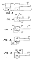
- a portion of a high density interconnect circuit 10 is shown in a plan view of a substrate 12 having a plurality of substrate contact pads 16 disposed thereon and of two integrated circuits (ICs) 20 bonded thereto.
- Each of the integrated circuit chips 20 has a plurality of chip contact pads 22 disposed thereon.
- Typical pad dimensions and spacings for the integrated circuits 20 are chip contact pads 22 which are 4 mils (100 microns) square and which are located on 8 mil (200 micron) centers, i.e. contact pads 4 mils square which are separated by 4 mil spaces.
- the illustrated part of the structure is a small portion of the 9 ICs and 40 substrate contact pads present in the complete structure.
- a dielectric layer (not shown) is disposed over the substrate 12, the chips 20 and the contact pads 22 of the chips.
- Figure 2 illustrates an ideal metallization pattern in accordance with the related European application 87311351.8 comprised of individual conductive runs 30 having vias 32 to contact pads 22 of the integrated circuit chips 20 and vias 36 for contact to the substrate contact pads 16.
- the wires which run horizontally in the figure are in one layer and the wires which run vertically in the figure are in a different layer and are connected where necessary through via holes in the intervening dielectric layer which are located at via pads 31.
- the via pads 31 of the conductive runs where a via hole to a different layer of metal is located are exaggerated in size as compared to the chip contact pads.
- These enlargements at vias are typically about 2.4 mils (0.06 mm) square and are for the purpose of ensuring that the via hole is located entirely over the underlying metal and entirely under the overlying metal.
- the conductive runs 30 are typically 1 mil (25 microns) wide.
- a picture frame region 18 is established around each of the integrated circuit chips 20 in which adaptive modification of the ideal metallization pattern is provided to compensate for tolerances in chip placement in accordance with the related application.
- the ideal conductor layout illustrated in Figure 2 employs 200 micron (8 mil) wide picture frames. This enables the system of the related application to compensate for placement errors of up to 4 mils since the maximum tolerance on chip placement is preferably one half of the picture frame width in order to prevent adaptation of conductors within the picture frame from violating design rules on conductor spacing. Routing the ideal wiring shown in Figure 2 required two hours of CPU time to perform the routing for the entire system using the "Omnicards" routing software and involved several unsuccessful attempts at routing which were unable to complete all routes.
- Figure 3 is a plan view illustration similar to that in Figure 2 in which the two illustrated integrated circuit chips are displaced from their ideal locations, the upper chip being displaced downward to the right and the lower chip being displaced upward to the left and rotated counter clockwise.
- conductive runs 30 have been modified within the picture frame area 18 as at 33 to properly connect the conductors of the shifted/rotated ideal pattern which is maintained in ideal alignment with the integrated circuit chips over the integrated circuit chips to the conductors of the ideal pattern which is maintained outside the picture frame 18.
- a plan view of the same portion of the same high density interconnect structure with an illustrative metallization pattern in accordance with the present invention is illustrated generally at 110 in Figure 4.
- the horizontal and vertical wires in the figure are generally in different layers except for short legs which do not interfere with routing.
- tolerances on the placement of the integrated circuit chips with respect to their ideal locations on the substrate 12 are compensated by (1) inclusion of a chip contact island in the overlying metal layer which overlaps the chip contact pad in both the ideal position and all displaced positions of the chip contact pad which are within established placement tolerances of that ideal position and (2) by movement of the via hole which connects the chip contact pad to the chip contact island in accordance with the actual position of the chip contact pad.
- the pattern of the conductive runs 130 in Figure 4 is different from the pattern of conductive runs 30 in Figure 2.
- chip contact islands 134 are provided in accordance with the present invention.
- substrate contact islands 138 are provided at the ends of conductive runs which are disposed in alignment with contact pads 16 on the substrate 12.
- the substrate contact islands 138 are similar to the chip contact islands 134 except for being substantially larger.
- the substrate contact pads 16 may be part of circuitry which is disposed on said substrate, may be portions of or connected to contact pads intended for wire bonding of the substrate into a larger external circuit or may comprise or be connected to edge connector contacts intended for insertion in an edge connecter to connect the substrate to external circuitry, or any other appropriate conductive structure.
- typical pad dimensions and spacings for the integrated circuits 20 are square chip contact pads which are 4 mils (100 microns) on a side and which are located on 8 mil (200 micron) centers, that is, contact pads which are 4 mils square and spaced apart by 4 mils.
- the contact islands 134 in the conductive metallization are preferably also 4 mils (100 microns) square and spaced apart by 4 mils (100 microns).
- the width of the conductive runs 130 is preferably such that, without violating the design rules on spacings, a conductive run may be run between two adjacent chip contact islands 134.
- One specification which is preferred for the conductive runs 130 is that they be 1 mil (25 microns) wide and spaced from adjacent conductors by at least 1.5 mils (37.5 microns). This specification is met for a single conductor passing between two adjacent chip contact islands for 4 mil pads on 8 mil centers.
- the via holes may preferably be square and formed by dithering of a laser in the manner taught in U.S. patent application Serial No. 310,149, filed February 14, 1989, by C.W. Eichelberger et al. and entitled "Laser Beam Scanning Method for Forming Via Holes in Polymer Materials". (European Patent Application 90301498.3 - RD 18932). This application is incorporated herein by reference.
- the actual location of the chip contact pads is preferably determined by an optical system in which reference marks on the substrate such as particular substrate contact pads or index marks are used as location reference points with respect to which the actual location of each chip and its contact pads are determined after the chips have been bonded to the substrate.
- This determination of any displacements of the chip contact pads from their ideal locations is preferably made prior to applying the first dielectric overlayer and is made prior to drilling via holes in the first dielectric layer in preparation for formation of the first metallization layer of the high density interconnect system.
- the actual position of the chip contact pads is preferably determined after bonding of the chips in accordance with the technique described in the above-identified, related, incorporated by reference U.S.
- a chip contact pad 122 is illustrated at the left of the figure.
- This chip contact pad is a square having a side length Lp.
- a chip contact island 134 and conductive run 130 are illustrated.
- the chip contact island 134 is a square with a side length of L ; .
- Lp L ; .
- the chip contact island 134 is located in the ideal position for its associated contact pad, since the overall ideal wiring pattern is preferably always positioned in its ideal location relative to the substrate except under special circumstances which are discussed subsequently, but which are not applicable here.
- chip contact island 134 is shown disposed over the chip contact pad 122 in their ideal alignment, that is, their alignment when the chip is positioned in its ideal location in which the chip contact island and the chip contact pad are perfectly aligned.
- a contact via 132 is illustrated in phantom in its ideal location in the center of both the chip contact pad 122 and the chip contact island 134.
- the contact via 132 may preferably be a square 1 mil on a side, but alternatively, may be circular or other desired shape. It will be noted that the via hole 132 is substantially smaller than either the chip contact pad 122 or the chip contact island 134.
- the via hole is preferably 1 mil (0.025 mm) square.
- the contact pad 122 is shown displaced from its ideal location about 1 mil to the left and about 1 mil downward in the figure.
- the via hole 132 in Figure 7 is displaced downward and to the left from the center of the contact island 134 and upward to the right from the center of the contact pad 122 and disposed essentially in the center of the overlap between the chip contact island 134 and the chip contact pad 122 and midway between the centers of the chip contact pad 122 and the chip contact island 134.
- the positions of via hole 132 are determined in accordance with the actual chip contact pad locations and the position in which the ideal first metallization layer will be positioned.
- the positioning accuracy of that metallization layer is much more precise that the accuracy with which a pick and place machine can, at this time, place the chip.
- both the underlying metal pattern and the overlying metal pattern are ideal metal patterns without any localized displacements in either pattern whereas, in the present embodiment, each of the integrated circuits may be displaced relative to its ideal position, thus, contact is being made to a non-ideal pattern.
- the contact frame is provided to compensate for inaccuracies in the overall alignment of the ideal second metal pattern with respect to the ideal first metal pattern whereas, in the present embodiment, the alignment of the second metal pattern is much more precise than the size of the features in the first level metal and the contact island is to compensate for individual displacements of the various integrated circuits from their ideal positions
- the contact frames are sized in accordance with the accuracy with which the metal pattern they form a part of can be positioned.
- the metal layer is precisely positioned and the contact islands are sized with respect to the chip placement accuracy.
- the via holes are individually positioned on each of the chip contact pads in accordance with the direction and extent to which that chip contact is displaced from its ideal position to ensure that, with the overlying metal layer in its ideal position, the via hole will lie entirely over the chip contact pad and entirely under the chip contact island.
- a via hole which is smaller than the chip contact pad
- a via hole the size of the chip contact pad could be used. In that way, the chip contact island would contact the chip contact pad everywhere within their overlap.
- Such a large via hole is not preferred because (1) its area of 16 square mils (0.01 square mm) is 16 times the area of a 1 mil square (0.000625 square mm) via hole and takes 16 times as long to make, (2) introduces the possibility of the drilled via hole extending off the chip contact pad where the laser which drills the via hole may adversely affect the structure of the integrated circuit, (3) does not eliminate the requirement for adaptation of the via hole location if it is to be aligned with the chip contact pad, (4) if the position of such a large via hole is not adapted, i.e.
- the via hole will extend off the chip contact pad.
- Having the via hole extend off a chip contact pad raises reliability concerns because, when the laser light which drills the via hole strikes the metal of the chip contact pad, it is substantially completely reflected, and thus does not affect the chip's structure. However, if that laser light strikes other portions of the chip, it may be absorbed and may adversely affect the structure of the chip (including its passivation). Further, extending the via hole off the chip contact pad exposes the area off the contact pad to the etchant used to clean out the via hole, raises the possibility of trapping undesired materials in the structure and may result in crazing of the dielectric.
- the first metal layer has its ideal configuration, no adaptation is required in subsequent metal layers or in the via hole pattern which connects those layers to the first metal layer. This simplifies both the initial routing of these higher layers and their fabrication.
- This is an additional advantage of this adaptation technique since in the technique of the related application, every metallization layer and every set of via holes must be adapted in order to properly connect to wiring which overlaps the integrated circuit chips. That requires extra effort both in the original routing of the wires and in their fabrication, since a standard pattern cannot be used.
- the substrate contact islands and the substrate contact pads are substantially larger than the chip contact pads, typically being about 25 mils (0.625 mm) in their smaller dimensions. Consequently, it is considered preferable to connect the substrate contact islands to the substrate contact pds by three via holes each.
- the substrate contact islands and substrate contact pads are large enough that their overlap is assured even if the metallization pattern were displaced a substantial distance from its ideal location.
- the placement tolerance maximum T max is an unsigned magnitude
- the placement with respect to the ideal location is ⁇ 3 mils or an overall placement accuracy of 6 mils is required. Consequently, maximum alignment tolerance is achieved by determining the position of each integrated circuit chip and its contact pads with respect to the ideal location thereof and determining the maximum displacement in the positive X-direction among the chip pads and the maximum displacement in the negative X-direction among the chip contact pads. If the difference in these displacements is less than 6 mils, then the X-direction displacement of chips can be compensated by shifting the ideal metallization pattern even if the displacement in one of the directions is greater than 3 mils.
- the chip displacement from the ideal location can be compensated by shifting the ideal metallization pattern in the Y-direction, if necessary.
- the chip pad which is displaced the greatest distance in the positive X-direction is displaced only 1 mil, then a maximum chip contact displacement in the negative X-direction of 5 mils may be accommodated by shifting the ideal metallization pattern relative to the substrate.
- T max the maximum displacement of chip contact pads from their ideal location exceeds T max , one or more chips may be removed and repositioned as has been discussed, or the size of the chip contact islands may be increased from 4 mils square to 6 mils square, thereby increasing T max to 4 mils and the maximum overall chip misalignment which may be accommodated to a total of 8 mils.
- this increase in island size prevents a conductive run from passing between two of the chip contact islands because the chip contact islands are then spaced apart by only 2 mils and the design rules require a 4 mil space for the passage of a conductive run. In order to provide conductive runs extending "between" the contact islands, an additional layer of metallization would be required.
- chip contact islands are then connected to the underlying chip contact pads by appropriately located via holes and an ideal metallization pattern is disposed in successive layers thereover. That is, the contact islands are disposed in an intermediate layer between the chip contact pads and the conductive runs of the ideal metallization. If desired, a separate contact island may still be present in the same layer as the conductive runs themselves, whereby the contact islands in the intermediate layer are intermediate contact islands.
- these enlarged separate contact islands may be provided within that ground plane or power plane as illustrated in Figure 10 where a power plane 140 has a plurality of chip contact islands 144 disposed therein with gaps 142 between the power plane itself and individual contact island which are not part of the power plane.
- Four power plane contact islands 44p are shown in phantom in Figure 10. These phantom locations are where a contact island would be located in association with the other contact islands 144 in a structure which had no power plane and in which the contact island 144 were being provided in a separate layer.
- Substrate contact islands 148 are preferably provided in this same layer in order that all the via holes produced for a given metal layer may be of the same depth.
- the substrate contact islands 148 are not needed for alignment purposes, omission of them would require that via holes extending to the substrate contact island from the next higher metal layer pass through two dielectric layers. However, with the substrate contact islands present, the substrate contact islands are connected by via holes through one dielectric layer to the substrate contact pads and the next higher metal layer is connected to the substrate contact islands 148 by a via hole through a single dielectric layer.
Landscapes
- Internal Circuitry In Semiconductor Integrated Circuit Devices (AREA)
- Design And Manufacture Of Integrated Circuits (AREA)
Applications Claiming Priority (1)
| Application Number | Priority Date | Filing Date | Title |
|---|---|---|---|
| US07/361,623 US5019997A (en) | 1989-06-05 | 1989-06-05 | Adaptive lithography accommodation of tolerances in chip positioning in high density interconnection structures |
Publications (1)
| Publication Number | Publication Date |
|---|---|
| EP0471122A1 true EP0471122A1 (de) | 1992-02-19 |
Family
ID=23422794
Family Applications (1)
| Application Number | Title | Priority Date | Filing Date |
|---|---|---|---|
| EP90308959A Withdrawn EP0471122A1 (de) | 1989-06-05 | 1990-08-15 | Hochdichte Verbindungsstrukturen und Herstellungsmethoden für solche |
Country Status (2)
| Country | Link |
|---|---|
| US (1) | US5019997A (de) |
| EP (1) | EP0471122A1 (de) |
Cited By (3)
| Publication number | Priority date | Publication date | Assignee | Title |
|---|---|---|---|---|
| EP0662713A3 (de) * | 1993-12-14 | 1995-08-30 | Ibm | Minimale Auffangflächen für Keramikvias in Keramiksubstraten. |
| FR2773264A1 (fr) * | 1997-12-30 | 1999-07-02 | St Microelectronics Sa | Portion de circuit integre |
| EP1381080A3 (de) * | 2002-07-09 | 2005-08-03 | Shinko Electric Industries Co. Ltd. | Platine mit eingebetteten Komponenten und ihre Herstellungsmethode |
Families Citing this family (28)
| Publication number | Priority date | Publication date | Assignee | Title |
|---|---|---|---|---|
| US5367467A (en) * | 1990-11-27 | 1994-11-22 | Dainippon Screen Mfg. Co., Ltd. | Method of and apparatus for inspecting width of wiring line on printed board |
| US5309370A (en) * | 1990-12-13 | 1994-05-03 | Vlsi Technology, Inc. | Method for placement of connectors used interconnecting circuit components in an integrated circuit |
| JPH05120373A (ja) * | 1991-10-30 | 1993-05-18 | Mitsubishi Electric Corp | 設計検証装置 |
| US5341310A (en) * | 1991-12-17 | 1994-08-23 | International Business Machines Corporation | Wiring layout design method and system for integrated circuits |
| US5315485A (en) * | 1992-09-29 | 1994-05-24 | Mcnc | Variable size capture pads for multilayer ceramic substrates and connectors therefor |
| US5446649A (en) * | 1992-12-31 | 1995-08-29 | International Business Machines Corporation | Data-hiding and skew scan for unioning of shapes in electron beam lithography post-processing |
| US5682323A (en) | 1995-03-06 | 1997-10-28 | Lsi Logic Corporation | System and method for performing optical proximity correction on macrocell libraries |
| US5844810A (en) * | 1995-05-30 | 1998-12-01 | General Electric Company | Scaled adaptive lithography |
| US5841102A (en) * | 1996-11-08 | 1998-11-24 | W. L. Gore & Associates, Inc. | Multiple pulse space processing to enhance via entrance formation at 355 nm |
| US6023041A (en) * | 1996-11-08 | 2000-02-08 | W.L. Gore & Associates, Inc. | Method for using photoabsorptive coatings and consumable copper to control exit via redeposit as well as diameter variance |
| US5868950A (en) * | 1996-11-08 | 1999-02-09 | W. L. Gore & Associates, Inc. | Method to correct astigmatism of fourth yag to enable formation of sub 25 micron micro-vias using masking techniques |
| US6103992A (en) | 1996-11-08 | 2000-08-15 | W. L. Gore & Associates, Inc. | Multiple frequency processing to minimize manufacturing variability of high aspect ratio micro through-vias |
| US5910255A (en) * | 1996-11-08 | 1999-06-08 | W. L. Gore & Associates, Inc. | Method of sequential laser processing to efficiently manufacture modules requiring large volumetric density material removal for micro-via formation |
| JP2000505948A (ja) * | 1996-11-08 | 2000-05-16 | ダブリュ.エル.ゴア アンド アソシエイツ,インコーポレイティド | 公称位置合せを向上させるための基準手法を用いる方法 |
| US5863446A (en) * | 1996-11-08 | 1999-01-26 | W. L. Gore & Associates, Inc. | Electrical means for extracting layer to layer registration |
| US5965043A (en) * | 1996-11-08 | 1999-10-12 | W. L. Gore & Associates, Inc. | Method for using ultrasonic treatment in combination with UV-lasers to enable plating of high aspect ratio micro-vias |
| AU4902897A (en) * | 1996-11-08 | 1998-05-29 | W.L. Gore & Associates, Inc. | Method for improving reliability of thin circuit substrates by increasing the T of the substrate |
| JP2001525120A (ja) * | 1996-11-08 | 2001-12-04 | ダブリュ.エル.ゴア アンド アソシエイツ,インコーポレイティド | ブラインドおよびスルーの両マイクロ―ヴァイアの入口の品質を向上するために吸光コーティングを用いる方法 |
| JP4234205B2 (ja) * | 1996-11-08 | 2009-03-04 | ダブリュ.エル.ゴア アンド アソシエイツ,インコーポレイティド | 電子アセンブリおよび電子物品内でのヴァイアのインダクタンスを低減する方法 |
| US5973290A (en) * | 1997-02-26 | 1999-10-26 | W. L. Gore & Associates, Inc. | Laser apparatus having improved via processing rate |
| US7027629B2 (en) * | 1999-11-05 | 2006-04-11 | Agilent Technologies, Inc. | Method of extracting locations of nucleic acid array features |
| US20030220746A1 (en) * | 2002-05-21 | 2003-11-27 | Srinka Ghosh | Method and system for computing and applying a global, multi-channel background correction to a feature-based data set obtained from scanning a molecular array |
| US7211736B2 (en) * | 2003-10-31 | 2007-05-01 | Hewlett-Packard Development Company, L.P. | Connection pad layouts |
| US20060040287A1 (en) * | 2004-06-02 | 2006-02-23 | Corson John F | Method and system for quantifying random errors and any spatial-intensity trends present in microarray data sets |
| US7302348B2 (en) | 2004-06-02 | 2007-11-27 | Agilent Technologies, Inc. | Method and system for quantifying and removing spatial-intensity trends in microarray data |
| US7528069B2 (en) * | 2005-11-07 | 2009-05-05 | Freescale Semiconductor, Inc. | Fine pitch interconnect and method of making |
| DE102006010523B3 (de) * | 2006-02-20 | 2007-08-02 | Siemens Ag | Verfahren zur Herstellung von planaren Isolierschichten mit positionsgerechten Durchbrüchen mittels Laserschneiden und entsprechend hergestellte Vorrichtungen |
| US7824965B2 (en) * | 2007-08-07 | 2010-11-02 | Skyworks Solutions, Inc. | Near chip scale package integration process |
Family Cites Families (6)
| Publication number | Priority date | Publication date | Assignee | Title |
|---|---|---|---|---|
| US4295149A (en) * | 1978-12-29 | 1981-10-13 | International Business Machines Corporation | Master image chip organization technique or method |
| US4613941A (en) * | 1985-07-02 | 1986-09-23 | The United States Of America As Represented By The Secretary Of The Army | Routing method in computer aided customization of a two level automated universal array |
| JPS62108593A (ja) * | 1985-11-06 | 1987-05-19 | 日本電気株式会社 | 多層配線基板 |
| US4866508A (en) * | 1986-09-26 | 1989-09-12 | General Electric Company | Integrated circuit packaging configuration for rapid customized design and unique test capability |
| JPS63245952A (ja) * | 1987-04-01 | 1988-10-13 | Hitachi Ltd | マルチチップモジュ−ル構造体 |
| US4901136A (en) * | 1987-07-14 | 1990-02-13 | General Electric Company | Multi-chip interconnection package |
-
1989
- 1989-06-05 US US07/361,623 patent/US5019997A/en not_active Expired - Lifetime
-
1990
- 1990-08-15 EP EP90308959A patent/EP0471122A1/de not_active Withdrawn
Non-Patent Citations (2)
| Title |
|---|
| IEDM'83, CH1973-7/80000-0542, 1983, pages 542-545, IEEE, New York, US; R.M. GEFFKEN: "Multi-level metallurgy for master image structured logic" * |
| IEEE TRANSACTIONS ON COMPONENTS, HYBRIDS AND MANUFACTURING TECHNOLOGY, vol. 12, no. 4, December 1989, pages 646-649; A.T. BARFKNECHT et al.: "Multichip packaging technology with laser-patterned interconnects" * |
Cited By (7)
| Publication number | Priority date | Publication date | Assignee | Title |
|---|---|---|---|---|
| EP0662713A3 (de) * | 1993-12-14 | 1995-08-30 | Ibm | Minimale Auffangflächen für Keramikvias in Keramiksubstraten. |
| US5916451A (en) * | 1993-12-14 | 1999-06-29 | International Business Machines Corporation | Minimal capture pads applied to ceramic vias in ceramic substrates |
| FR2773264A1 (fr) * | 1997-12-30 | 1999-07-02 | St Microelectronics Sa | Portion de circuit integre |
| EP0930652A1 (de) * | 1997-12-30 | 1999-07-21 | STMicroelectronics SA | Teilstück der Metallisierung einer integrierten Schaltung |
| EP1381080A3 (de) * | 2002-07-09 | 2005-08-03 | Shinko Electric Industries Co. Ltd. | Platine mit eingebetteten Komponenten und ihre Herstellungsmethode |
| US7707713B2 (en) | 2002-07-09 | 2010-05-04 | Shinko Electric Industries Co., Ltd. | Component-embedded circuit board fabrication method |
| US7793412B2 (en) | 2002-07-09 | 2010-09-14 | Shinko Electric Industries Co., Ltd. | Component-embedded board fabrication method |
Also Published As
| Publication number | Publication date |
|---|---|
| US5019997A (en) | 1991-05-28 |
Similar Documents
| Publication | Publication Date | Title |
|---|---|---|
| US5019997A (en) | Adaptive lithography accommodation of tolerances in chip positioning in high density interconnection structures | |
| JP3895768B2 (ja) | シリコンセグメントのための垂直相互接続方法 | |
| US5357403A (en) | Adaptive lithography in a high density interconnect structure whose signal layers have fixed patterns | |
| US5127570A (en) | Flexible automated bonding method and apparatus | |
| US5258920A (en) | Locally orientation specific routing system | |
| EP0516402B1 (de) | Mit elektrischen Leitungen versehenes Substrat und dessen Herstellungsverfahren | |
| US4700214A (en) | Electrical circuitry | |
| US5055907A (en) | Extended integration semiconductor structure with wiring layers | |
| EP0341001B1 (de) | Verfahren zum Herstellen von grossen Halbleiterschaltungen | |
| EP0018489A2 (de) | Modul für eine Anordnung von integrierten Schaltungschips mit fly-wire-Verbindungen nach Bedarf | |
| US4720470A (en) | Method of making electrical circuitry | |
| EP0615290A2 (de) | Verbindungsgeometrie mit reduzierter Kapazitätsladung für elektronische Strukturen | |
| US5710063A (en) | Method for improving the alignment of holes with other elements on a printed circuit board | |
| WO1993019487A1 (en) | Integrated circuit module having microscopic self-alignment features | |
| JP2001127240A (ja) | 半導体装置の製造方法 | |
| EP0795906A2 (de) | Elektronischer Schaltungsaufbau und seine Herstellung | |
| EP0182222B1 (de) | Integrierte Halbleiterschaltungsanordnung in Polycell-Technik | |
| WO1985002751A1 (en) | Partially aligned multi-layered circuitry | |
| KR100267483B1 (ko) | 바이어 홀 개구 검사용 첵크 패턴 | |
| WO1990009093A1 (en) | Extended integration semiconductor structure and method of making the same | |
| CN115881546A (zh) | 芯片互联的封装结构及其封装方法 | |
| EP0171783A2 (de) | Modulträger und Modul, der diesen Träger benutzt und Verfahren zur Behandlung derselben | |
| TW202314878A (zh) | 晶片互聯的封裝結構及其封裝方法 | |
| JPH04106967A (ja) | 高密度相互接続回路及び製造方法 | |
| EP0253833B1 (de) | Mehrschichtige gedruckte verdrahtungsplatte |
Legal Events
| Date | Code | Title | Description |
|---|---|---|---|
| PUAI | Public reference made under article 153(3) epc to a published international application that has entered the european phase |
Free format text: ORIGINAL CODE: 0009012 |
|
| AK | Designated contracting states |
Kind code of ref document: A1 Designated state(s): DE FR GB IT |
|
| 17P | Request for examination filed |
Effective date: 19911220 |
|
| STAA | Information on the status of an ep patent application or granted ep patent |
Free format text: STATUS: THE APPLICATION HAS BEEN WITHDRAWN |
|
| 18W | Application withdrawn |
Withdrawal date: 19920222 |