EP0469583A2 - Halbleitersubstrat mit einer vollständig dielektrischen Isolationsstruktur und Verfahren dessen Herstellung - Google Patents
Halbleitersubstrat mit einer vollständig dielektrischen Isolationsstruktur und Verfahren dessen Herstellung Download PDFInfo
- Publication number
- EP0469583A2 EP0469583A2 EP91112887A EP91112887A EP0469583A2 EP 0469583 A2 EP0469583 A2 EP 0469583A2 EP 91112887 A EP91112887 A EP 91112887A EP 91112887 A EP91112887 A EP 91112887A EP 0469583 A2 EP0469583 A2 EP 0469583A2
- Authority
- EP
- European Patent Office
- Prior art keywords
- semiconductor substrate
- insulating film
- grooves
- oxide film
- island regions
- Prior art date
- Legal status (The legal status is an assumption and is not a legal conclusion. Google has not performed a legal analysis and makes no representation as to the accuracy of the status listed.)
- Withdrawn
Links
Images


Classifications
-
- H—ELECTRICITY
- H01—ELECTRIC ELEMENTS
- H01L—SEMICONDUCTOR DEVICES NOT COVERED BY CLASS H10
- H01L21/00—Processes or apparatus adapted for the manufacture or treatment of semiconductor or solid state devices or of parts thereof
- H01L21/70—Manufacture or treatment of devices consisting of a plurality of solid state components formed in or on a common substrate or of parts thereof; Manufacture of integrated circuit devices or of parts thereof
- H01L21/71—Manufacture of specific parts of devices defined in group H01L21/70
- H01L21/76—Making of isolation regions between components
- H01L21/762—Dielectric regions, e.g. EPIC dielectric isolation, LOCOS; Trench refilling techniques, SOI technology, use of channel stoppers
- H01L21/76224—Dielectric regions, e.g. EPIC dielectric isolation, LOCOS; Trench refilling techniques, SOI technology, use of channel stoppers using trench refilling with dielectric materials
-
- H—ELECTRICITY
- H01—ELECTRIC ELEMENTS
- H01L—SEMICONDUCTOR DEVICES NOT COVERED BY CLASS H10
- H01L21/00—Processes or apparatus adapted for the manufacture or treatment of semiconductor or solid state devices or of parts thereof
- H01L21/70—Manufacture or treatment of devices consisting of a plurality of solid state components formed in or on a common substrate or of parts thereof; Manufacture of integrated circuit devices or of parts thereof
- H01L21/71—Manufacture of specific parts of devices defined in group H01L21/70
- H01L21/76—Making of isolation regions between components
- H01L21/762—Dielectric regions, e.g. EPIC dielectric isolation, LOCOS; Trench refilling techniques, SOI technology, use of channel stoppers
- H01L21/7624—Dielectric regions, e.g. EPIC dielectric isolation, LOCOS; Trench refilling techniques, SOI technology, use of channel stoppers using semiconductor on insulator [SOI] technology
- H01L21/76264—SOI together with lateral isolation, e.g. using local oxidation of silicon, or dielectric or polycristalline material refilled trench or air gap isolation regions, e.g. completely isolated semiconductor islands
- H01L21/76283—Lateral isolation by refilling of trenches with dielectric material
-
- H—ELECTRICITY
- H01—ELECTRIC ELEMENTS
- H01L—SEMICONDUCTOR DEVICES NOT COVERED BY CLASS H10
- H01L21/00—Processes or apparatus adapted for the manufacture or treatment of semiconductor or solid state devices or of parts thereof
- H01L21/70—Manufacture or treatment of devices consisting of a plurality of solid state components formed in or on a common substrate or of parts thereof; Manufacture of integrated circuit devices or of parts thereof
- H01L21/71—Manufacture of specific parts of devices defined in group H01L21/70
- H01L21/76—Making of isolation regions between components
- H01L21/762—Dielectric regions, e.g. EPIC dielectric isolation, LOCOS; Trench refilling techniques, SOI technology, use of channel stoppers
- H01L21/7624—Dielectric regions, e.g. EPIC dielectric isolation, LOCOS; Trench refilling techniques, SOI technology, use of channel stoppers using semiconductor on insulator [SOI] technology
- H01L21/76264—SOI together with lateral isolation, e.g. using local oxidation of silicon, or dielectric or polycristalline material refilled trench or air gap isolation regions, e.g. completely isolated semiconductor islands
- H01L21/76286—Lateral isolation by refilling of trenches with polycristalline material
-
- H—ELECTRICITY
- H01—ELECTRIC ELEMENTS
- H01L—SEMICONDUCTOR DEVICES NOT COVERED BY CLASS H10
- H01L21/00—Processes or apparatus adapted for the manufacture or treatment of semiconductor or solid state devices or of parts thereof
- H01L21/70—Manufacture or treatment of devices consisting of a plurality of solid state components formed in or on a common substrate or of parts thereof; Manufacture of integrated circuit devices or of parts thereof
- H01L21/71—Manufacture of specific parts of devices defined in group H01L21/70
- H01L21/76—Making of isolation regions between components
- H01L21/763—Polycrystalline semiconductor regions
-
- H—ELECTRICITY
- H01—ELECTRIC ELEMENTS
- H01L—SEMICONDUCTOR DEVICES NOT COVERED BY CLASS H10
- H01L21/00—Processes or apparatus adapted for the manufacture or treatment of semiconductor or solid state devices or of parts thereof
- H01L21/70—Manufacture or treatment of devices consisting of a plurality of solid state components formed in or on a common substrate or of parts thereof; Manufacture of integrated circuit devices or of parts thereof
- H01L21/71—Manufacture of specific parts of devices defined in group H01L21/70
- H01L21/76—Making of isolation regions between components
- H01L21/762—Dielectric regions, e.g. EPIC dielectric isolation, LOCOS; Trench refilling techniques, SOI technology, use of channel stoppers
- H01L21/7624—Dielectric regions, e.g. EPIC dielectric isolation, LOCOS; Trench refilling techniques, SOI technology, use of channel stoppers using semiconductor on insulator [SOI] technology
- H01L21/76264—SOI together with lateral isolation, e.g. using local oxidation of silicon, or dielectric or polycristalline material refilled trench or air gap isolation regions, e.g. completely isolated semiconductor islands
- H01L21/76275—Vertical isolation by bonding techniques
-
- H—ELECTRICITY
- H01—ELECTRIC ELEMENTS
- H01L—SEMICONDUCTOR DEVICES NOT COVERED BY CLASS H10
- H01L21/00—Processes or apparatus adapted for the manufacture or treatment of semiconductor or solid state devices or of parts thereof
- H01L21/70—Manufacture or treatment of devices consisting of a plurality of solid state components formed in or on a common substrate or of parts thereof; Manufacture of integrated circuit devices or of parts thereof
- H01L21/71—Manufacture of specific parts of devices defined in group H01L21/70
- H01L21/76—Making of isolation regions between components
- H01L21/762—Dielectric regions, e.g. EPIC dielectric isolation, LOCOS; Trench refilling techniques, SOI technology, use of channel stoppers
- H01L21/7624—Dielectric regions, e.g. EPIC dielectric isolation, LOCOS; Trench refilling techniques, SOI technology, use of channel stoppers using semiconductor on insulator [SOI] technology
- H01L21/76264—SOI together with lateral isolation, e.g. using local oxidation of silicon, or dielectric or polycristalline material refilled trench or air gap isolation regions, e.g. completely isolated semiconductor islands
- H01L21/76289—Lateral isolation by air gap
Definitions
- the present invention relates to a semiconductor substrate having a complete dielectric isolation structure and a method of making the same.
- a p-n junction or a dielectric isolation structure has been well known as an isolation structure.
- the dielectric isolation structure has the following advantages as compared to the p-n junction isolation structure;
- a method using direct bonding of two substrates a method of epitaxially growing silicon on a sapphire substrate called an SOS, and a method of recrystallizing amorphous silicon deposited on an insulating film have been known.
- the following method has been also known. That is, a part of a silicon wafer is etched to form an oxide film, and a polysilicon layer is deposited thereon. Thereafter, the resultant structure is lapped from its lower surface, thereby obtaining island regions supported by the polysilicon layer and isolated from one another.
- the method using bonding of two substrates is an excellent one having the following characteristics. That is, a thick silicon layer having a high quality is provided as an active layer, and the bonded wafer has a relatively low warpage.
- a method of making a dielectric isolation substrate using the above bonding will be described below with reference to Figs. 6A to 6D.
- Silicon wafers 31 and 32 each having at least one mirror surface are prepared, an oxide film 33 is formed on the surface of one of the silicon wafers 31 and 32.
- the two wafers 31 and 32 are heat-treated to be integrally boned, while the oxide film 33 is interposed therebetween. Thereafter, the surface of the silicon wafer 32, which serves as an active layer for providing circuit elements therein, is lapped to have a predetermined thickness (Fig. 6A).
- the surface of the silicon wafer 32 is selectively etched by anisotropic etching to form a groove 34 having a V-shaped section, and an oxide film 35 is formed on the surface of the silicon wafer 32 (Fig. 6B).
- a polysilicon layer 36 is deposited on the entire surface of the oxide film 35 to bury the groove 34 therewith (Fig. 6C).
- the deposited surface of the polysilicon layer 36 is lapped by lapping or the like so as to be planarized, thereby obtaining a dielectric isolation substrate (Fig. 6D).
- the thickness of the oxide film 33 is defined by a dielectric breakdown voltage and a capacitance, which are required between the active layer, on which circuit elements are to be provided, and the wafer 31 serving as a support substrate.
- the oxide film 33 having a thickness of about several /1.m is required for circuit element characteristics.
- the thickness of the oxide film for dielectric isolation must be structurally increased.
- Fig. 7 shows a relationship between an isolation oxide film thickness (/1.m) and warpage d (/1.m) of a wafer, wherein a shift d between the edge and the center of the wafer having a diameter of 100 mm is measured.
- the warpage is increased in proportion to the thickness of the oxide film. This relationship can be obtained when the wafer has a large diameter.
- the warpage d is proportional to the square of the wafer diameter, the substrate is affected by the warpage as increasing the diameter.
- a fine PEP photoetching process
- an object of the present invention to provide a semiconductor substrate which has a dielectric isolation structure with a reduced warpage.
- a semiconductor substrate having dielectrically isolated island regions which comprises a first semiconductor substrate for providing circuit elements, a second semiconductor substrate for supporting the first semiconductor substrate, a first insulating film located between the first and second semiconductor substrates, a plurality of grooves formed in the first semiconductor substrate to expose a surface of the second semiconductor substrate, and a second insulating film formed on the exposed surface of the second semiconductor substrate.
- a plurality of island regions are provided above the second semiconductor substrate through the first insulating film and the second insulating film is thinner than the first insulating film so as to reduce unwanted warpage produced in the semiconductor substrate.
- a semiconductor substrate according to the first embodiment of the present invention and steps in making the same will be described below.
- 20 n-type silicon wafers 11 each having a diameter of 125 mm, a thickness of 625 ⁇ m, a crystal plane of (100), and a resistivity p of about 0.15 Q. cm are prepared, and a thermal oxide film 13 having a thickness of 2 ⁇ m is formed on each of the silicon wafers 11.
- 20 silicon wafers 12 each having a diameter of 125 mm, a thickness of 525 ⁇ m, a crystal plane of (100), and a resistivity of about 40 Q. cm are prepared.
- each of the wafers 11 and each of the wafers 12 are bonded to each other in a clean atmosphere.
- the resultant structure is heat-treated in a mixed gas atmosphere, composed of an 0 2 gas and an N 2 gas, at a temperature of 1,100°C for 2 hours, thereby providing one complete wafer.
- the mixed gas is obtained by mixing the 0 2 gas with the N 2 gas at a ratio of 1 : 4.
- the silicon wafer 11 is lapped to have a thickness of, e.g., 25 ⁇ m (Fig. 1A).
- An oxide film 14 is formed on the surface of the wafer 11.
- An etching mask 15 of a photoresist layer is formed on the oxide film 14 by well-known techniques (Fig. 1 B).
- the resultant structure is anisotropically etched by a potassium hydroxide solution, using the remained oxide film 14 as a mask.
- V-shaped grooves 16 are then formed in the wafer 11, thereby providing a plurality of isolated island regions 111 (Fig. 1 C).
- the oxide films 13 located on bottoms of the grooves 16 are then removed by an aqueous solution composed of hydrofluoric acid and pure water at a mixing ratio of 1 : 2, thereby exposing the surface of the wafer 12 (Fig. 1 D).
- the oxide film 13 located on the bottom of each groove 16 was removed from each of the 10 wafers of the 20 wafers, and the oxide film 13 was not removed from each of the 10 remaining wafers.
- a measurement of the warpage was then carried out on both wafer groups, using a surface roughness gauge. The following results were obtained. That is, one wafer group with the oxide film 13 had a convex warpage of about 60 ⁇ m, but the other wafer group without the oxide film 13 had the warpage of about 30 tim.
- An oxide film 17 having a thickness of 0.5 ⁇ m is formed on the bottom of each groove 16 and the surface of each island region 111 (Fig. 1 E).
- a polysilicon layer 18 is deposited on the entire surface of the resultant structures to have a thickness of 50 ⁇ m (Fig. 1 F).
- the island regions 111 are lapped to have a thickness of 15 ⁇ m, thereby providing a dielectric isolation substrate (Fig. 1 G).
- both substrate groups had the dielectric breakdown voltage of 1300 - 1500 V between each island region 111 and the support wafer 12, and had also the similar capacitance values to each other.
- the oxide film 13 located on each of the bottoms of the grooves 16 is completely removed as shown in Fig. 1D.
- the substrate may be etched so as to leave a thin oxide film 130 as shown in Fig. 1 H.
- the thickness of the oxide film 17 located between the bottom portions of the grooves 16 and the wafer 12 is sufficiently reduced as compared with the oxide film 13 located between the wafer 11 and wafer 12, the amount of the warpage can be reduced.
- the thickness of the wafer 11 can be precisely controlled, processing precision can be improved, and the diameter of the wafer 11 can be increased.
- the dielectric isolation substrate has the small warpage, fine PEP or the like can be easily performed by lithography apparatus in the wafer process.
- the thickness of the oxide film 17 is reduced, good results can be obtained.
- the area of the groove or the area of the thin oxide film is increased, good advantages can be obtained.
- the oxide film formed on the bottom of each groove was once removed by etching, and the exposed support wafer surface was oxidized to provide a thin oxide film thereon.
- the area of the groove and the film thickness were changed to investigate the advantages.
- the warpage was reduced because the thickness of the oxide film formed on the bottom of the groove was decreased. The reason for the reduction of the warpage did not merely depend upon the reduction of the total amount of the oxide films.
- the result shows that a stress is released by isolating the thick oxide film into a large number of parts.
- the ratio of the grooves to the substrate area exceeded 1/3, conspicuous advantages could be obtained.
- the thickness of the oxide film 17 was increased, crystal defects occurred in the island regions 111 and the wafer 12. Since the island regions 111 and the oxide film 13 serve as a mask when the bottom of the groove is oxidized, crystal defects may occur by a mechanism similar to that of LOCOS defects. The defects do not occur when the thickness of the oxide film 17 is 90% or less of that of the oxide film 13.
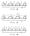
- FIG. 2A the oxide film 17 of the first embodiment is not formed on the bottom of the groove 16, and the oxide film 17 are formed on only the side surface of the groove 16.
- the groove 16 having a V-shaped section is used in the first embodiment, a groove 16 having vertical side surface and formed by, e.g., an RIE (Reactive Ion Etching) technique are used as shown in Fig. 3.
- the thin film 17 is formed on only the side surface of the groove 16.
- the second embodiment since an oxide film is entirely removed from the bottom of the groove 16, the warpage of the wafer is greatly reduced, and a polysilicon layer 18 buried in the groove 16 can be electrically connected to the support wafer 12.
- the polysilicon layer 18 buried in the groove 16 and the support wafer 12 are generally kept at a ground potential.
- a wiring layer since the polysilicon layers 18 is insulated from the wafer 12 by the oxide film 17, a wiring layer must be arranged to decrease the potential of the polysilicon layer 18 to the ground potential. However, according to the second embodiment, this wiring layer is not necessary.
- the grooves 16 between the island regions 111 may be buried with an insulating material 19 such as resin.
- the semiconductor substrate has a structure similar to the structure shown in Figs. 1G, 2A, and 2B.
- grooves 16 are not buried with a polysilicon layer 18, and the isolation is performed while exposing the groove 16.
- the structure is often used in a case where the thickness of the wafer 11 or the island region 111 is thin.
- the same advantages as described in the first embodiment can be obtained.
- the present invention is not limited to the above embodiments, and various modifications can be provided.
- the substrate obtained such that silicon substrates are integrally bonded to each other through the oxide film by the direct bonding technique has been described in the above embodiments.
- the present invention can be applied to a substrate obtained such that silicon substrates are integrally bonded through a dielectric film having a thermal expansion coefficient different from that of the silicon substrates by another bonding method such as electrostatic bonding techniques and CVD glass bonding techniques.
- the thick oxide film is located only between island regions, which are made of silicon and in which circuit elements are to be formed, and the support substrate, and the oxide film on the bottom of the groove for isolating the island regions from each other has a thin thickness or is removed. Therefore, the warpage of the wafer can be greatly reduced, processing precision can be improved, and the wafer having the large diameter can be obtained.
Landscapes
- Engineering & Computer Science (AREA)
- Physics & Mathematics (AREA)
- Condensed Matter Physics & Semiconductors (AREA)
- General Physics & Mathematics (AREA)
- Manufacturing & Machinery (AREA)
- Computer Hardware Design (AREA)
- Microelectronics & Electronic Packaging (AREA)
- Power Engineering (AREA)
- Chemical & Material Sciences (AREA)
- Crystallography & Structural Chemistry (AREA)
- Element Separation (AREA)
Applications Claiming Priority (2)
| Application Number | Priority Date | Filing Date | Title |
|---|---|---|---|
| JP203563/90 | 1990-07-31 | ||
| JP2203563A JPH0488657A (ja) | 1990-07-31 | 1990-07-31 | 半導体装置とその製造方法 |
Publications (2)
| Publication Number | Publication Date |
|---|---|
| EP0469583A2 true EP0469583A2 (de) | 1992-02-05 |
| EP0469583A3 EP0469583A3 (en) | 1993-02-03 |
Family
ID=16476208
Family Applications (1)
| Application Number | Title | Priority Date | Filing Date |
|---|---|---|---|
| EP19910112887 Withdrawn EP0469583A3 (en) | 1990-07-31 | 1991-07-31 | Semiconductor substrate with complete dielectric isolation structure and method of making the same |
Country Status (2)
| Country | Link |
|---|---|
| EP (1) | EP0469583A3 (de) |
| JP (1) | JPH0488657A (de) |
Cited By (3)
| Publication number | Priority date | Publication date | Assignee | Title |
|---|---|---|---|---|
| WO1993026041A1 (en) * | 1992-06-17 | 1993-12-23 | Harris Corporation | Bonded wafer processing |
| CN100510824C (zh) * | 2005-02-10 | 2009-07-08 | 奔瑞公司 | 用于光纤管的密封的管接合件 |
| CN113675220A (zh) * | 2020-07-30 | 2021-11-19 | 台湾积体电路制造股份有限公司 | 半导体器件及其形成方法 |
Families Citing this family (4)
| Publication number | Priority date | Publication date | Assignee | Title |
|---|---|---|---|---|
| US5457068A (en) * | 1992-11-30 | 1995-10-10 | Texas Instruments Incorporated | Monolithic integration of microwave silicon devices and low loss transmission lines |
| KR100319615B1 (ko) * | 1999-04-16 | 2002-01-09 | 김영환 | 반도체 장치에서의 소자격리방법 |
| US7262112B2 (en) * | 2005-06-27 | 2007-08-28 | The Regents Of The University Of California | Method for producing dislocation-free strained crystalline films |
| JP2011192882A (ja) * | 2010-03-16 | 2011-09-29 | Nec Corp | 半導体構造及び半導体装置及びその製造方法 |
Citations (3)
| Publication number | Priority date | Publication date | Assignee | Title |
|---|---|---|---|---|
| EP0182032A2 (de) * | 1984-09-19 | 1986-05-28 | Kabushiki Kaisha Toshiba | SoI-Halbleiteranordnung und Verfahren zu ihrer Herstellung |
| EP0296754A2 (de) * | 1987-06-18 | 1988-12-28 | Kabushiki Kaisha Toshiba | Verfahren zur Herstellung von Halbleiteranordnungen mit Gräben als Isolationszonen |
| EP0437950A2 (de) * | 1989-12-20 | 1991-07-24 | Fujitsu Limited | Halbleiteranordnung mit einer Silizium-auf-Isolatorstruktur und Verfahren zu deren Herstellung |
-
1990
- 1990-07-31 JP JP2203563A patent/JPH0488657A/ja active Pending
-
1991
- 1991-07-31 EP EP19910112887 patent/EP0469583A3/en not_active Withdrawn
Patent Citations (3)
| Publication number | Priority date | Publication date | Assignee | Title |
|---|---|---|---|---|
| EP0182032A2 (de) * | 1984-09-19 | 1986-05-28 | Kabushiki Kaisha Toshiba | SoI-Halbleiteranordnung und Verfahren zu ihrer Herstellung |
| EP0296754A2 (de) * | 1987-06-18 | 1988-12-28 | Kabushiki Kaisha Toshiba | Verfahren zur Herstellung von Halbleiteranordnungen mit Gräben als Isolationszonen |
| EP0437950A2 (de) * | 1989-12-20 | 1991-07-24 | Fujitsu Limited | Halbleiteranordnung mit einer Silizium-auf-Isolatorstruktur und Verfahren zu deren Herstellung |
Non-Patent Citations (3)
| Title |
|---|
| IEDM- TECHNICAL DIGEST 13-14 DEC. 1982 IEEE 1982 NEW-YORK pages 237 - 240 R.D. RUNG ET AL. 'DEEP TRENCH ISOLATED CMOS devices' * |
| IEDM-TECNICAL DIGEST, 13-14 DEC. 1982, IEEE 1982 NEW-YORK pages 58 - 61 H. GOTO ET AL. 'AN ISOLATION TECHNOLOGY FOR HIGH PERFORMANCE BIPOLAR MEMORIES--IO-II' * |
| PESC 1988 RECORD 19TH ANNUAL IEEE POWER ELECTRONICS SPECIALISTS CONFERENCE APRIL 11-14, 1988 TOKYO pages 1325 - 1329 , XP00092660 A. NAKAGAWA ET AL. 'HIGH VOLTAGE, NEW DRIVER IC TECHNIQUE BASED ON SILICON WAFER DIRECT-BONDING (SDB)' * |
Cited By (8)
| Publication number | Priority date | Publication date | Assignee | Title |
|---|---|---|---|---|
| WO1993026041A1 (en) * | 1992-06-17 | 1993-12-23 | Harris Corporation | Bonded wafer processing |
| US5780311A (en) * | 1992-06-17 | 1998-07-14 | Harris Corporation | bonded wafer processing |
| US5801084A (en) * | 1992-06-17 | 1998-09-01 | Harris Corporation | Bonded wafer processing |
| CN100510824C (zh) * | 2005-02-10 | 2009-07-08 | 奔瑞公司 | 用于光纤管的密封的管接合件 |
| CN113675220A (zh) * | 2020-07-30 | 2021-11-19 | 台湾积体电路制造股份有限公司 | 半导体器件及其形成方法 |
| EP3951847A1 (de) * | 2020-07-30 | 2022-02-09 | Taiwan Semiconductor Manufacturing Company, Ltd. | Mehrschichtige isolationsstruktur für hochspannungs-silizium-auf-isolator-vorrichtung |
| TWI784571B (zh) * | 2020-07-30 | 2022-11-21 | 台灣積體電路製造股份有限公司 | 積體電路裝置及其形成方法 |
| US11682578B2 (en) | 2020-07-30 | 2023-06-20 | Taiwan Semiconductor Manufacturing Co., Ltd. | Multilayer isolation structure for high voltage silicon-on-insulator device |
Also Published As
| Publication number | Publication date |
|---|---|
| EP0469583A3 (en) | 1993-02-03 |
| JPH0488657A (ja) | 1992-03-23 |
Similar Documents
| Publication | Publication Date | Title |
|---|---|---|
| US6211039B1 (en) | Silicon-on-insulator islands and method for their formation | |
| US5426072A (en) | Process of manufacturing a three dimensional integrated circuit from stacked SOI wafers using a temporary silicon substrate | |
| US6174784B1 (en) | Technique for producing small islands of silicon on insulator | |
| KR100413911B1 (ko) | 실리콘-온-절연체 영역 및 벌크 영역 제조 방법 및 조밀하게 패터닝된 실리콘-온-절연체 제조 방법 | |
| US4507158A (en) | Trench isolated transistors in semiconductor films | |
| JP2717979B2 (ja) | 絶縁体上に薄い単結晶シリコン島状部を製造する方法 | |
| JPH01315159A (ja) | 誘電体分離半導体基板とその製造方法 | |
| US4851366A (en) | Method for providing dielectrically isolated circuit | |
| JPH01179342A (ja) | 複合半導体結晶体 | |
| US5438015A (en) | Silicon-on-insulator technique with buried gap | |
| EP0469583A2 (de) | Halbleitersubstrat mit einer vollständig dielektrischen Isolationsstruktur und Verfahren dessen Herstellung | |
| JPH0883837A (ja) | 半導体装置及びその製造方法 | |
| US4026736A (en) | Integrated semiconductor structure with combined dielectric and PN junction isolation including fabrication method therefor | |
| US4571818A (en) | Isolation process for high-voltage semiconductor devices | |
| KR950003899B1 (ko) | 반도체 기판의 제조 방법 | |
| KR890003146B1 (ko) | 유전체 격리구조를 가진 보상 반도체장치를 제조하는 방법 | |
| EP0661735B1 (de) | Verfahren zur Herstellung integrierter Schaltungen, insbesondere intelligenter Leistungsanordnungen | |
| JPS5828731B2 (ja) | ゼツエンキバンジヨウヘノ シリコンソウサクセイホウホウ | |
| US6432792B1 (en) | Substrate and method for manufacturing the same | |
| JPH02260442A (ja) | 誘電体分離型半導体基板 | |
| JPS6362252A (ja) | 誘電体絶縁分離基板の製造方法 | |
| JP3013632B2 (ja) | 誘電体分離基板の製造方法 | |
| EP1193752A1 (de) | Verfahren zur Herstellung einer lokalisierten Silizium-auf-Isolator-Struktur | |
| JP2755215B2 (ja) | Soi基板の製造方法 | |
| JPS6155253B2 (de) |
Legal Events
| Date | Code | Title | Description |
|---|---|---|---|
| PUAI | Public reference made under article 153(3) epc to a published international application that has entered the european phase |
Free format text: ORIGINAL CODE: 0009012 |
|
| 17P | Request for examination filed |
Effective date: 19910731 |
|
| AK | Designated contracting states |
Kind code of ref document: A2 Designated state(s): DE FR GB IT |
|
| PUAL | Search report despatched |
Free format text: ORIGINAL CODE: 0009013 |
|
| AK | Designated contracting states |
Kind code of ref document: A3 Designated state(s): DE FR GB IT |
|
| 17Q | First examination report despatched |
Effective date: 19930405 |
|
| STAA | Information on the status of an ep patent application or granted ep patent |
Free format text: STATUS: THE APPLICATION IS DEEMED TO BE WITHDRAWN |
|
| 18D | Application deemed to be withdrawn |
Effective date: 19950613 |