EP0467971B1 - Komplementäre feldeffekt-transistorlogik mit hoher geschwindigkeit - Google Patents
Komplementäre feldeffekt-transistorlogik mit hoher geschwindigkeit Download PDFInfo
- Publication number
- EP0467971B1 EP0467971B1 EP90906650A EP90906650A EP0467971B1 EP 0467971 B1 EP0467971 B1 EP 0467971B1 EP 90906650 A EP90906650 A EP 90906650A EP 90906650 A EP90906650 A EP 90906650A EP 0467971 B1 EP0467971 B1 EP 0467971B1
- Authority
- EP
- European Patent Office
- Prior art keywords
- fet
- conductivity type
- inverter
- logic circuit
- load
- Prior art date
- Legal status (The legal status is an assumption and is not a legal conclusion. Google has not performed a legal analysis and makes no representation as to the accuracy of the status listed.)
- Expired - Lifetime
Links
- 230000000295 complement effect Effects 0.000 title claims abstract description 40
- 230000005669 field effect Effects 0.000 title claims description 7
- 230000003247 decreasing effect Effects 0.000 abstract description 3
- 230000008878 coupling Effects 0.000 description 14
- 238000010168 coupling process Methods 0.000 description 14
- 238000005859 coupling reaction Methods 0.000 description 14
- 238000010586 diagram Methods 0.000 description 8
- 239000011159 matrix material Substances 0.000 description 5
- 230000009471 action Effects 0.000 description 3
- 230000008901 benefit Effects 0.000 description 3
- 230000000694 effects Effects 0.000 description 3
- 230000004044 response Effects 0.000 description 3
- 230000007423 decrease Effects 0.000 description 2
- 230000006872 improvement Effects 0.000 description 2
- 239000004065 semiconductor Substances 0.000 description 2
- 230000008859 change Effects 0.000 description 1
- 238000009792 diffusion process Methods 0.000 description 1
- 230000003292 diminished effect Effects 0.000 description 1
- 150000002500 ions Chemical class 0.000 description 1
- 230000002427 irreversible effect Effects 0.000 description 1
- 239000002184 metal Substances 0.000 description 1
- 229910044991 metal oxide Inorganic materials 0.000 description 1
- 150000004706 metal oxides Chemical class 0.000 description 1
- 230000003068 static effect Effects 0.000 description 1
- 239000000758 substrate Substances 0.000 description 1
- 230000007704 transition Effects 0.000 description 1
Images

Classifications
-
- H—ELECTRICITY
- H03—ELECTRONIC CIRCUITRY
- H03K—PULSE TECHNIQUE
- H03K19/00—Logic circuits, i.e. having at least two inputs acting on one output; Inverting circuits
- H03K19/01—Modifications for accelerating switching
- H03K19/017—Modifications for accelerating switching in field-effect transistor circuits
- H03K19/01707—Modifications for accelerating switching in field-effect transistor circuits in asynchronous circuits
- H03K19/01721—Modifications for accelerating switching in field-effect transistor circuits in asynchronous circuits by means of a pull-up or down element
-
- H—ELECTRICITY
- H03—ELECTRONIC CIRCUITRY
- H03K—PULSE TECHNIQUE
- H03K19/00—Logic circuits, i.e. having at least two inputs acting on one output; Inverting circuits
- H03K19/02—Logic circuits, i.e. having at least two inputs acting on one output; Inverting circuits using specified components
- H03K19/08—Logic circuits, i.e. having at least two inputs acting on one output; Inverting circuits using specified components using semiconductor devices
- H03K19/094—Logic circuits, i.e. having at least two inputs acting on one output; Inverting circuits using specified components using semiconductor devices using field-effect transistors
- H03K19/0944—Logic circuits, i.e. having at least two inputs acting on one output; Inverting circuits using specified components using semiconductor devices using field-effect transistors using MOSFET or insulated gate field-effect transistors, i.e. IGFET
- H03K19/0948—Logic circuits, i.e. having at least two inputs acting on one output; Inverting circuits using specified components using semiconductor devices using field-effect transistors using MOSFET or insulated gate field-effect transistors, i.e. IGFET using CMOS or complementary insulated gate field-effect transistors
- H03K19/09482—Logic circuits, i.e. having at least two inputs acting on one output; Inverting circuits using specified components using semiconductor devices using field-effect transistors using MOSFET or insulated gate field-effect transistors, i.e. IGFET using CMOS or complementary insulated gate field-effect transistors using a combination of enhancement and depletion transistors
- H03K19/09485—Logic circuits, i.e. having at least two inputs acting on one output; Inverting circuits using specified components using semiconductor devices using field-effect transistors using MOSFET or insulated gate field-effect transistors, i.e. IGFET using CMOS or complementary insulated gate field-effect transistors using a combination of enhancement and depletion transistors with active depletion transistors
Definitions
- This invention relates to digital logic circuits of the kind that may be employed in integrated circuits, and more particularly to high speed, high density, low power complementary field effect transistor logic circuits.
- CMOS logic circuits Complementary Field Effect Transistor (FET) logic circuits, and in particular Complementary Metal Oxide Semiconductor (CMOS) logic circuits have become increasingly popular for high density integrated circuit logic, among other reasons because of their high density and low power dissipation.
- a typical CMOS logic gate is illustrated in Figure 1 of U.S. Patent No. 3,911,289 to Takemoto entitled MOS Type Semiconductor IC Device .
- a CMOS logic gate typically includes a driving stage having a plurality of FETs of a first conductivity type connected in parallel and a load stage comprising a like plurality of serially connected FETs of opposite conductivity type. Each logic signal input is applied simultaneously to a pair of transistors, one driver and one load.
- FIG. 3A of the aforementioned U.S. Patent No. 3,911,289 discloses an all parallel logic gate in which the serial load transistors are replaced by a first load which may be a MOS transistor or a resistor and a second load comprising a MOS transistor having opposite conductivity type from the driver stage transistors. The first and second loads are connected in parallel.
- a complementary MOS inverter is also provided between the output of the driving stage and a voltage source.
- Japanese Patent 60-236,322 to Yoshida entitled MOS Transistor Circuit is disclosed in Japanese Patent 60-236,322 to Yoshida entitled MOS Transistor Circuit .
- U.S. Patent No. 4,390,988 discloses a multiplexer having a plurality of driving stage FETs 25,27 and 29 connected between a common output 37 and a plurality of logic signal inputs X1, X2 and XM.
- IBM Technical Disclosure Bulletin, Vol. 28, No. 6, November 1985, pp. 2576 and 2577 describes a complementary inverter at T3 and T4 for use in a single ended cascade voltage switch (CVS).
- CVS cascade voltage switch
- the invention consists in a field effect transistor (FET) logic circuit comprising a driving stage including at least one FET of a first conductivity type, having at least one control electrode fro receiving logic input signals, the at least one driving stage FET being connected between a common output and a first potential level, a load FET of second conductivity type connected between a second potential level and said common output, and a complementary FET inverter comprising an FET of said first conductivity type and an FET of said second conductivity type, serially connected between said first and second potential levels, the input of said complementary inverter being connected to said common output and the output of said complementary inverter being connected to the control electrode of said load FET characterized by the product of the carrier mobility and the ratio of channel width to length of the inverter FET of said first conductivity type being greater than the product of the carrier mobility and the ratio of channel width to length of the inverter FET of said second conductivity type, so as to achieve a voltage transfer function for said complementary FET inverter which is skewed from
- the voltage transfer function of the complementary FET inverter is deliberately skewed, in contrast with a conventional symmetrical complementary inverter design.
- the product of the carrier mobility and the ratio of channel width to length of the inverter FET of the first conductivity type is four times the product of the carrier mobility and the ratio of channel width to length of the inverter FET of the second conductivity type.
- the voltage lift-off interval for the logic gate is dramatically decreased thereby improving the speed of the gate.
- the load FET of the second conductivity type, which is connected as an "inverted drain follower" is a depletion mode FET, additional pull-up transistors or resistors are not needed.
- the depletion mode FET provides the total lift-off function by providing a sustaining current to control snap-off. Power dissipation is thereby reduced while providing high speed and low device count. OR and AND circuits-may be provided.
- a second load FET of the second conductivity type may be provided which is connected between the second potential level and the common output, with the control electrode of the second load being connected to any one of the control electrodes of the driving stage FETs.
- the second load FET provides lift-off current only when the appropriate control electrode is activated, which minimizes idle power dissipation while increasing switching speed.
- An enhancement mode transistor is preferably employed.
- a second complementary FET inverter may be provided in which the voltage transfer function is maintained symmetrical i.e, it is not skewed.
- This second inverter is connected in parallel with the first inverter, with the output of the second inverter being connected to the control electrode of the second load FET and its input connected to the control electrode of the first load FET.
- the use of a second inverter also provides a complement output (i.e. NAND and NOR) for the logic gate.
- the second load FET may comprise a multigate FET with a respective one of the gate electrodes being connected to a respective one of the control electrodes of the driving stage FETs.
- this embodiment provides slightly slower switching speed because of the serial multigate load FET, essentially zero power consumption may be provided.
- a multigate FET and/or a series-parallel arrangement of FETs may also be substituted for at least one of the driving stage transistors to provide "matrix logic" circuits which implement complex logic functions.
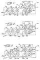
- Figure 1 is a circuit schematic diagram of an FET logic OR circuit according to the present invention.
- Figure 2 is a circuit schematic diagram of an FET logic AND circuit according to the present invention.
- Figure 3 is a circuit schematic diagram of an alternative embodiment of an FET logic OR circuit according to the present invention.
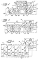
- Figure 4 is a circuit schematic diagram of another alternative embodiment of an FET logic OR circuit according to the present invention.
- Figure 5 is a circuit schematic diagram of yet another alternative embodiment of an FET logic OR gate of the present invention.
- Figure 6 is a circuit schematic diagram of an FET matrix logic circuit according to the present invention.
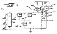
- Figure 7 is a circuit schematic diagram of an alternative embodiment of an FET matrix logic circuit according to the present invention.
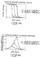
- FIGS 8A-8B illustrate transfer functions of complementary FET inverters Shown in Figure 1-7.
- Figure 9 illustrates the current voltage transfer function of an inverted drain follower load transistor Shown in Figures 1-7.
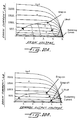
- FIG 10 illustrates switching diagrams for FET logic circuits Shown in Figures 1-7.
- Figure 11 illustrates the superposition of sustaining current and inverted drain follower load transistor current characteristics of the FET logic circuits Shown in Figures 1-7.
- the complementary FET inverter 14 is serially connected between V dd and ground, with the output 17 of the complementary inverter 14 being the output of the logic gate 10 .
- the output 17 is also connected to the gate 13a of inverted drain follower load transistor 13 .
- the gates 15a and 15b of the complementary inverter are also connected to the common output 16 .
- the product of the carrier mobility and the ratio of channel width to length of FET 14b is made substantially greater than the product of the carrier mobility and the ratio of width to length of the type FET 14a .
- ⁇ 14b Z 14b /L 14b >> ⁇ 14a Z 14a /L 14a
- ⁇ is the carrier mobility
- Z is the channel width
- L is the channel length of respective transistors 14a and 14b .
- FIG. 3 an alternative embodiment of an OR logic circuit according to the present invention is shown. It will be recognized by those having skill in the art that each of the circuits of Figures 3-7 may be provided in an AND configuration by interchanging the N- and P- devices and voltage terminals.
- the circuit of Figure 3 is identical with the circuit of Figure 1 except that an additional lift-off transistor 18 is provided, the gate 18a of which is connected to one of the gates 12 of the driving stage FETs.
- gate 18a is shown connected to gate 12b .
- lift-off transistor 18 is activated when and only when the connected logic gate 12b is up for an AND gate and down for an OR gate thereby minimizing idle power dissipation while increasing the switching speed of the logic circuit.
- Coupling inverter 19 comprises P- transistor 19a and N-transistor 19b , the gates 20a and 20b of which are coupled to gate 13a of inverted drain follower 13 .
- the output 22 of the second coupling inverter 19 is connected to a second inverted drain follower 21 which itself is connected between power supply voltage V dd and common output 16 . Accordingly, a compliment output 22 for the logic gate 10 is provided.
- the voltage transfer function of inverter 19 is not skewed; i.e. the transistor design parameters are substantially similar, in contrast with coupling inverter 14 for which the voltage transfer function is deliberately skewed.
- Figure 7 is identical to the structure of Figure 1 except that the single gate transistor of driving stage 11 is replaced by a multigate transistor 42 and a series/parallel combination of transistors 43-45 of driving stage 41 .
- FETs 43 and 44 are connected in parallel with one another and in series with FET 45 between common output 16 and ground. It will be understood by those having skill in the art that other combinations of FETs, in single gate, multigate, parallel, series and series/parallel configurations, may be provided to implement any desired complex logic function.
- the logic gate of Figure 7 implements the logic function 42a ⁇ 42b ⁇ 42c+(43a ⁇ 45a+44a ⁇ 45a)+(43a ⁇ 44a ⁇ 45a).
- the left hand voltage transfer function occurs at a significantly lower value of input voltage than a symmetric inverter design.
- saturation current of the N- channel transistor dominates saturation current capabilities of the P- channel device.
- the opposite situation occurs when the P- channel transistor design dominates saturation current of the N- channel device.
- these skewed responses are the required design criteria for complementary inverter 14 of Figures 1-7.
- the left hand voltage transfer curve criteria is a design criteria for all OR gates, for example as illustrated in Figures 1, 3, 4, 5, 6 and 7.
- the right hand criteria is a design criteria for AND gates as illustrated in Figure 2. If these critical design criteria are not utilized in the design of the coupling inverter, switching speed is reduced and idle power is high negating most of the benefits of all parallel logic.
- the skewed complementary inverter design minimizes the "lift-off" time described below in connection with the "snap-off" property of the present invention.
- the fast switching of the skewed inverter design is utilized to provide all logic circuits of the present invention with maximum switching power and minimum or zero idling power.
- inverted drain follower 13 is illustrated as a function of drain voltage, where channel length is 1 ⁇ m and channel width is 5 ⁇ m and the substrate is doped with 2e16 exceptor ions per cm3.
- the unique characteristic of inverter drain follower 13 is that zero drain current occurs at both extremes of drain voltage. Between these end point voltages a substantial drain current flows that functions to charge or discharge circuit capacitances.
- the area under the curves shown in Figure 9 is the capacitive charging power. The amount of available power is controlled by the physical dimensions of transistor 13 .
- the zero end point current character of the inverted drain follower insures that no drain current flows at either output level of the logic. No idle power is dissipated by an enhancement inverted drain follower 13 .
- a depletion mode inverter drain follower may also be provided in order to provide the total lift-off function by providing a sustaining current that controls the "snap-off" property of the logic circuits of the present invention.
- FIG 9. There are two plots illustrated in Figure 9. For curve A, it is assumed that the coupling inverter transfer function is linear. Curve B reflects the actual Fermi-Dirac type of transfer function typical of a CMOS type inverter.
- Figure 10 shows the switching action of logic circuits 10 according to the present invention.
- Figure 10 shows the combined plots of drain current flowing in a 1 ⁇ m N- channel inverted drain follower device 13 driven with different designs of coupling inverter 14 , and the drain current flowing in a 1 ⁇ m P-channel and logic gate input transistor.
- oxide thickness is 120 ⁇ .
- This switching property provides the logic circuits of the present invention with high tolerance to noise signals.
- the gate voltage of any selected driving transistor 11 must be above the snap-on value.
- Snap-on voltage is above the threshold voltage of the driving transistor 11 .
- the value of the snap-on gate voltage is controlled by the relative dimensions of the inverter drain follower 13 compared to any one of the driving transistors 11 .
- the product of the carrier mobility, and the ratio of channel width to length of the driving transistor 11 is made greater than the product of carrier mobility and the ratio of channel width to length of the load FET 13 .
- snap-on voltage Given the drain supply voltage of 5V, snap-on voltage will be 2.5V if the drain saturation current of a driving transistor 11 is exactly twice that of the inverted drain follower transistor 13 .
- second load transistor 18 of Figure 3 when second load transistor 18 of Figure 3 is switched on by the action of gate 12b returning to the down level, it provides a sustaining current for logic gate conduction current that controls the snap-off property of the logic gate of the present invention.
- transistor 18 When on, transistor 18 provides idle (pull-up) current when the OR gate is on and its output is at the down level.
- a similar situation occurs when the output of an AND gate is at the up level.
- a typical sustaining current flowing in transistor 18 is 10 ⁇ A and accounts for power dissipation typically of about 50 ⁇ watt per logic function.
- the multigate configuration of Figure 5 operates as described above, except no idle power is dissipated at either logic state up or down.
- the need for a separate lift-off transistor 18 is eliminated by making the inverted drain follower transistor 13 a depletion mode device, as shown in Figures 1 and 2.
- inverted drain follower transistor 13 is a depletion mode device a prescribed amount of sustaining current is caused to flow when the gate voltage of transistor 13 equals its source voltage.
- Figures 10A, 10B and 11 illustrate the effects of adding idle current to the inverted drain follower current voltage profile. A non-zero current is shown to flow in the circuit when the output terminal voltage reaches a maximum of V dd . This current is called the sustaining current and defines the snap-off current threshold. As gate voltage of the P- channel logic gate, for example, is decreased, drain current drops.
- the logic output voltage drops along the contour called the lift-off interval as shown in Figures 10B and 11.
- the lift-off interval adds delay time to overall switching performance and may be used for that purpose in some logic situations. However, this delay time must be held to a minimum value by using the skewed inverter design of the present invention to achieve the maximum switching rate.
- the magnitude of the sustaining current is controlled entirely by the width to length ratio of the enhancement transistors 18 or 13 , when used or the depletion mode design of transistor 13 . Any value of sustaining current may be selected by the design of transistor 18 however sustaining current should be lower than value chosen for the snap-on current described above in order to preserve the hysteresis effect.
- the snap-off current is usually a fraction of the snap-on current and accounts for the hysteresis property of the logic gates of the present invention.
- a typical logic function lift-off time is 0.5 x 10 ⁇ 9 seconds.
- Lift-off time depends inversely on the sustaining current and directly upon the lift-off voltage interval and therefore can be selected primarily by the degrees of inverter skew and the value of sustaining current.
- the capacitive charging power of the inverted drain follower 13 dominates and overall very fast switching times result. It is critical that the lift-off interval be made small by skewing the voltage transfer function of the complementary inverter 14 as has been described above. Otherwise the virtues of using the inverted drain follower 13 are greatly diminished.
Landscapes
- Engineering & Computer Science (AREA)
- Physics & Mathematics (AREA)
- Computer Hardware Design (AREA)
- Computing Systems (AREA)
- General Engineering & Computer Science (AREA)
- Mathematical Physics (AREA)
- Power Engineering (AREA)
- Logic Circuits (AREA)
- Junction Field-Effect Transistors (AREA)
- Light Receiving Elements (AREA)
- Solid State Image Pick-Up Elements (AREA)
- Transforming Light Signals Into Electric Signals (AREA)
Claims (20)
- Feldeffekttransistor (FET)-Logikschaltung, die aufweist:
eine Treiberstufe (11), die zumindest einen FET (11a-11n) eines ersten Leitungstyps enthält, welcher zumindest eine Steuerelektrode (12a-12n) zum Empfang von logischen Eingangssignalen aufweist und der zwischen einen gemeinsamen Ausgang (16) und einen ersten Potentialpegel geschaltet ist;
einen Last-FET (13) des zweiten Leitungstyps, der zwischen einen zweiten Potentialpegel (Vdd) und den gemeinsamen Ausgang (16) geschaltet ist; und
ein komplementäres FET-Invertierglied (14), das einen FET (14b) des ersten Leitungstyps und einen FET (14a) des zweiten Leitungstyps aufweist, die in Reihe zwischen den ersten und zweiten Potentialpegel geschaltet sind, wobei der Eingang des komplementären Invertierglieds (14) mit dem gemeinsamen Ausgang (16) und der Ausgang des komplementären Invertierglieds (14) mit der Steuerelektrode (13a) des Last-FETs (13) verbunden sind,
dadurch gekennzeichnet, daß das Produkt aus der Trägerbeweglichkeit und dem Verhältnis der Kanalweite zur Kanallänge des Invertierglied-FETs des ersten Leitungstyps größer als das Produkt aus der Trägerbeweglichkeit und dem Verhältnis der Kanalweite zur Kanallänge des Invertierglied-FETs (14a) des zweiten Leitungstyps ist, um dadurch für das komplementäre FET-Invertierglied (14) eine Spannungsübertragungsfunktion zu erzielen, die gegenüber einer symmetrischen Übertragungsfunktion relativ zu dem ersten und zweiten Potentialpegel schräg verläuft. - FET-Logikschaltung (10) nach Anspruch 1, die eine ODER-Schaltung ist, bei der der erste Leitungstyp der N-Leitungstyp und der zweite Leitungstyp der P-Leitungstyp sind.
- FET-Logikschaltung (10) nach Anspruch 1, die eine UND-Schaltung ist, bei der der erste Leitungstyp der P-Leitungstyp und der zweite Leitungstyp der N-Leitungstyp sind.
- FET-Logikschaltung (10) nach Anspruch 1, 2 oder 3, bei der die FETs (11a-11n ) der Teiberstufe Anreicherungs-FET-Typen sind.
- FET-Logikschaltung (10) nach Anspruch 4, bei der die FETs (11a-11n) der Treiberstufe Anreicherungs-FET-Typen mit induziertem Kanal sind.
- FET-Logikschaltung (10) nach irgendeinem der vorangehenden Ansprüchen, bei der das Produkt aus der Trägerbeweglichkeit und dem Verhältnis der Kanalweite zur Kanallänge des Invertierglied-FETs (14b) des ersten Leitungstyps das Vierfache des Produkts aus der Trägerbeweglichkeit und dem Verhältnis der Kanalweite zur Kanallänge des Invertierglied-FETs (14a) des zweiten Leitungstyps ist.
- FET-Logikschaltung (10) nach irgendeinem der vorangehenden Ansprüche, bei der der Last-FET ein Verarmungs-FET-Typ ist.
- FET-Logikschaltung (10) nach irgendeinem der vorangehenden Ansprüche, bei der der Last-FET (13) geringfügig leitet, wenn dessen Steuerelektrode (13a) in der Nähe des zweiten Potentialpegels (Vdd) liegt, um einen Dauerstrom für die Logikschaltung zu erzeugen.
- FET-Logikschaltung (10) nach irgendeinem der vorangehenden Ansprüche, bei der der Last-FET (13) stark leitet, wenn seine Steuerelektrode (13a) in der Nähe des ersten Potentials liegt, um einen schnellen Einschaltstrom für die Logikschaltung (10) zu erzeugen.
- FET Logikschaltung (10) nach irgendeinem der vorangehenden Ansprüche, die einen zweiten Last-FET (18) des zweiten Leitungstyps aufweist, der zwischen den zweiten Potentialpegel (Vdd) und den gemeinsamen Ausgang (16) geschaltet ist und dessen Steuerelektrode (18a) mit einer der Steuerelektroden (12a-12n) der FETs (11a-11n) der Treiberstufe verbunden ist.
- FET-Logikschaltung nach irgendeinem der vorangehenden Ansprüche, bei der das Produkt aus der Trägerbeweglichkeit und dem Verhältnis der Kanalweite zur Kanallänge der FETs (11a-11n) der Treiberstufe größer ist als das Produkt aus der Trägerbeweglichkeit und dem Verhältnis der Kanalweite zur Kanallänge des Last-FETs (13).
- FET-Logischaltung (10) nach irgendeinem der vorangehenden Ansprüche, die aufweist:
einen zweiten Last-FET (21) des zweiten Leitungstyps, der zwischen das zweite Potential (Vdd) und den gemeinsamen Ausgang (16) geschaltet ist; und
ein zweites komplementäres FET-Invertierglied (19), das einen FET (19b) des ersten Leitungstyps und einen FET (19a) des zweiten Leitungstyps aufweist, die zwischen den ersten und den zweiten Potentialpegel in Reihe geschaltet sind, wobei der Ausgang des zweiten komplementären FET-Invertierglieds (19) mit der Steuerelektrode des zweiten Last-FETs (21) verbunden ist. - FET-Logikschaltung (10) nach Anspruch 12, bei der das Produkt aus der Trägerbeweglichkeit und dem Verhältnis der Kanalweite zur Kanallänge des FETs (19b) des ersten Leitungstyps des zweiten komplementären Invertierglieds gleich dem Produkt aus der Trägerbeweglichkeit und dem Verhältnis der Kanalweite zur Kanallänge des FETs (19a) des zweiten Leitungstyps vom zweiten komplementären Invertierglied ist.
- FET-Logikschaltung (10) nach Anspruch 12 oder 13, bei der der zweite Last-FET (23) einen FET mit mehreren Gate-Elektroden (23a-23n) aufweist, von denen jeweils eine mit jeweils einer der Steuerelektroden (12a-12n) der FETs (11a-11n) der Treiberstufe verbunden ist.
- FET-Logikschaltung (10) nach Anspruch 14, bei der der zweite Last-FET (23) ein Mehrfachgate-Fermischwellen-FET ist.
- FET-Logikschaltung (10) nach irgendeinem der vorangehenden Ansprüche, bei der wenigstens ein Teiberstufen-FET ( 11a-11n) einen Treiberstufen-FET (31a-31n) aufweist, der mehrere Steuerelektroden (32a-32z) zum Empfang logischer Eingangssignale hat.
- FET-Logikschaltung (10) nach Anspruch 16, bei der der genannte Treiberstufen-FET (31a-31n) mit den mehreren Steuerelektroden einen Mehrfachgate-Fermischwellen-FET aufweist.
- FET-Logikschaltung (10) nach irgend einem der vorangehenden Ansprüche, bei der zumindest zwei Treiberstufen-FETs (11a-11n, 32a-32n) parallel zueinander zwischen den gemeinsamen Ausgang (16) und den ersten Potentialpegel geschaltet sind.
- FET-Logikschaltung (10) nach irgendeinem der vorangehenden Ansprüche, bei der wenigstens zwei FETs ( 43, 45) der Treiberstufe in Reihe zwischen den gemeinsamen Ausgang (16) und den ersten Potentialpegel geschaltet sind.
- FET-Logikschaltung (10) nach irgendeinem der vorangehenden Ansprüche, bei der wenigstens drei FETs (43, 44, 45) der Treiberstufe in einer Reihen/ Parallelschaltung zwischen den gemeinsamen Ausgang (16) und den ersten Potentialpegel geschaltet sind.
Applications Claiming Priority (3)
| Application Number | Priority Date | Filing Date | Title |
|---|---|---|---|
| US338280 | 1989-04-14 | ||
| US07/338,280 US5001367A (en) | 1989-04-14 | 1989-04-14 | High speed complementary field effect transistor logic circuits |
| PCT/US1990/001957 WO1990013181A1 (en) | 1989-04-14 | 1990-04-10 | High speed complementary field effect transistor logic circuits |
Publications (2)
| Publication Number | Publication Date |
|---|---|
| EP0467971A1 EP0467971A1 (de) | 1992-01-29 |
| EP0467971B1 true EP0467971B1 (de) | 1994-10-19 |
Family
ID=23324152
Family Applications (1)
| Application Number | Title | Priority Date | Filing Date |
|---|---|---|---|
| EP90906650A Expired - Lifetime EP0467971B1 (de) | 1989-04-14 | 1990-04-10 | Komplementäre feldeffekt-transistorlogik mit hoher geschwindigkeit |
Country Status (8)
| Country | Link |
|---|---|
| US (1) | US5001367A (de) |
| EP (1) | EP0467971B1 (de) |
| JP (1) | JP2839368B2 (de) |
| AT (1) | ATE113146T1 (de) |
| AU (1) | AU5523690A (de) |
| CA (1) | CA2051103C (de) |
| DE (1) | DE69013498T2 (de) |
| WO (1) | WO1990013181A1 (de) |
Families Citing this family (10)
| Publication number | Priority date | Publication date | Assignee | Title |
|---|---|---|---|---|
| US5387827A (en) * | 1990-01-20 | 1995-02-07 | Hitachi, Ltd. | Semiconductor integrated circuit having logic gates |
| US5247212A (en) * | 1991-01-31 | 1993-09-21 | Thunderbird Technologies, Inc. | Complementary logic input parallel (clip) logic circuit family |
| JPH0685653A (ja) * | 1992-05-06 | 1994-03-25 | Sgs Thomson Microelectron Inc | バスキーパ特徴を有するレシーバ回路 |
| US5307352A (en) * | 1993-03-01 | 1994-04-26 | Advanced Micro Devices, Inc. | Switch matrix multiplexers |
| US5517133A (en) * | 1993-07-14 | 1996-05-14 | Sun Microsystems, Inc. | Multiple-input OR-gate employing a sense amplifier |
| US5612638A (en) * | 1994-08-17 | 1997-03-18 | Microunity Systems Engineering, Inc. | Time multiplexed ratioed logic |
| US5654651A (en) * | 1994-10-18 | 1997-08-05 | Hitachi, Ltd. | CMOS static logic circuit |
| US5654652A (en) * | 1995-09-27 | 1997-08-05 | Cypress Semiconductor Corporation | High-speed ratio CMOS logic structure with static and dynamic pullups and/or pulldowns using feedback |
| US5737270A (en) * | 1996-07-15 | 1998-04-07 | International Business Machines Corporation | Precharged wordline decoder with locally-controlled clock |
| US8933746B1 (en) | 2013-07-10 | 2015-01-13 | Astronics Advanced Electronic Systems Corp. | Parallel FET solid state relay utilizing commutation FETs |
Family Cites Families (25)
| Publication number | Priority date | Publication date | Assignee | Title |
|---|---|---|---|---|
| US3728556A (en) * | 1971-11-24 | 1973-04-17 | United Aircraft Corp | Regenerative fet converter circuitry |
| US3911289A (en) * | 1972-08-18 | 1975-10-07 | Matsushita Electric Industrial Co Ltd | MOS type semiconductor IC device |
| US4053792A (en) * | 1974-06-27 | 1977-10-11 | International Business Machines Corporation | Low power complementary field effect transistor (cfet) logic circuit |
| JPS5759689B2 (de) * | 1974-09-30 | 1982-12-16 | Citizen Watch Co Ltd | |
| UST952012I4 (de) * | 1976-01-20 | 1976-11-02 | ||
| JPS5336167A (en) * | 1976-09-16 | 1978-04-04 | Nippon Telegr & Teleph Corp <Ntt> | Logical operation circuit |
| US4080539A (en) * | 1976-11-10 | 1978-03-21 | Rca Corporation | Level shift circuit |
| US4216390A (en) * | 1978-10-04 | 1980-08-05 | Rca Corporation | Level shift circuit |
| US4258272A (en) * | 1979-03-19 | 1981-03-24 | National Semiconductor Corporation | TTL to CMOS input buffer circuit |
| IT1139929B (it) * | 1981-02-06 | 1986-09-24 | Rca Corp | Circuito generatore di impulsi utilizzante una sorgente di corrente |
| US4390988A (en) * | 1981-07-14 | 1983-06-28 | Rockwell International Corporation | Efficient means for implementing many-to-one multiplexing logic in CMOS/SOS |
| US4491741A (en) * | 1983-04-14 | 1985-01-01 | Motorola, Inc. | Active pull-up circuit |
| US4567385A (en) * | 1983-06-22 | 1986-01-28 | Harris Corporation | Power switched logic gates |
| JPS60236322A (ja) * | 1984-05-09 | 1985-11-25 | Mitsubishi Electric Corp | Mosトランジスタ回路 |
| US4649296A (en) * | 1984-07-13 | 1987-03-10 | At&T Bell Laboratories | Synthetic CMOS static logic gates |
| DE3511625A1 (de) * | 1985-03-29 | 1986-10-02 | Siemens AG, 1000 Berlin und 8000 München | Verdrahtete oder-anordnung |
| US4785204A (en) * | 1985-06-21 | 1988-11-15 | Mitsubishi Denki Kabushiki Kaisha | Coincidence element and a data transmission path |
| US4810906A (en) * | 1985-09-25 | 1989-03-07 | Texas Instruments Inc. | Vertical inverter circuit |
| US4764691A (en) * | 1985-10-15 | 1988-08-16 | American Microsystems, Inc. | CMOS programmable logic array using NOR gates for clocking |
| US4645952A (en) * | 1985-11-14 | 1987-02-24 | Thomson Components-Mostek Corporation | High speed NOR gate |
| US4701643A (en) * | 1986-03-24 | 1987-10-20 | Ford Microelectronics, Inc. | FET gate current limiter circuits |
| US4701642A (en) * | 1986-04-28 | 1987-10-20 | International Business Machines Corporation | BICMOS binary logic circuits |
| US4798979A (en) * | 1986-09-23 | 1989-01-17 | Honeywell Inc. | Schottky diode logic for E-mode FET/D-mode FET VLSI circuits |
| US4877976A (en) * | 1987-03-13 | 1989-10-31 | Gould Inc. | Cascade FET logic circuits |
| US4990974A (en) | 1989-03-02 | 1991-02-05 | Thunderbird Technologies, Inc. | Fermi threshold field effect transistor |
-
1989
- 1989-04-14 US US07/338,280 patent/US5001367A/en not_active Expired - Lifetime
-
1990
- 1990-04-10 JP JP2506467A patent/JP2839368B2/ja not_active Expired - Lifetime
- 1990-04-10 AU AU55236/90A patent/AU5523690A/en not_active Abandoned
- 1990-04-10 AT AT90906650T patent/ATE113146T1/de not_active IP Right Cessation
- 1990-04-10 WO PCT/US1990/001957 patent/WO1990013181A1/en not_active Ceased
- 1990-04-10 DE DE69013498T patent/DE69013498T2/de not_active Expired - Lifetime
- 1990-04-10 EP EP90906650A patent/EP0467971B1/de not_active Expired - Lifetime
- 1990-04-10 CA CA002051103A patent/CA2051103C/en not_active Expired - Lifetime
Non-Patent Citations (1)
| Title |
|---|
| Arthur H. Seidman: "INTEGRATED CIRCUITS APPLICATION HANDBOOK", John Wiley & Sons, New York * Chichester * Brisbane * Toronto * Singapore, 1983, pages 95 - 111 * |
Also Published As
| Publication number | Publication date |
|---|---|
| ATE113146T1 (de) | 1994-11-15 |
| DE69013498D1 (de) | 1994-11-24 |
| JP2839368B2 (ja) | 1998-12-16 |
| JPH05504661A (ja) | 1993-07-15 |
| US5001367A (en) | 1991-03-19 |
| CA2051103A1 (en) | 1990-10-15 |
| WO1990013181A1 (en) | 1990-11-01 |
| EP0467971A1 (de) | 1992-01-29 |
| AU5523690A (en) | 1990-11-16 |
| DE69013498T2 (de) | 1995-03-30 |
| CA2051103C (en) | 1998-06-30 |
Similar Documents
| Publication | Publication Date | Title |
|---|---|---|
| US7592841B2 (en) | Circuit configurations having four terminal JFET devices | |
| US4575648A (en) | Complementary field effect transistor EXCLUSIVE OR logic gates | |
| KR930000968B1 (ko) | 반도체 집적회로 | |
| EP0739097B1 (de) | MOSFET Schaltung und ihre Anwendung in einer CMOS Logikschaltung | |
| EP0243603B1 (de) | Binäre logische Schaltung | |
| US5089722A (en) | High speed output buffer circuit with overlap current control | |
| US4514649A (en) | High-entrance high-speed logic operator which has a complex digital function and utilizes at least one quasi-normally off MESFET | |
| JPH05267603A (ja) | 集積回路 | |
| US4682055A (en) | CFET inverter having equal output signal rise and fall times by adjustment of the pull-up and pull-down transconductances | |
| US4028556A (en) | High-speed, low consumption integrated logic circuit | |
| JP3463269B2 (ja) | Mosfet回路 | |
| US5001367A (en) | High speed complementary field effect transistor logic circuits | |
| US4430583A (en) | Apparatus for increasing the speed of a circuit having a string of IGFETs | |
| US4489246A (en) | Field effect transistor logic circuit having high operating speed and low power consumption | |
| US4587446A (en) | Field effect transistor output circuit operable by a reduced amount of current | |
| US4954730A (en) | Complementary FET circuit having merged enhancement/depletion FET output | |
| KR790001774B1 (ko) | 논리회로 | |
| US5250855A (en) | Fast logic circuits | |
| US4851713A (en) | Fast CMOS NAND gate circuit | |
| JP2800336B2 (ja) | 半導体アナログスイッチ | |
| JP3523611B2 (ja) | 差動型論理回路 | |
| CA1244529A (en) | Depletion mode fet logic system | |
| USRE32515E (en) | Apparatus for increasing the speed of a circuit having a string of IGFETS | |
| US6559700B2 (en) | Semiconductor integrated circuit | |
| EP0023210B1 (de) | Logische puffer-schaltung mit drei zuständen |
Legal Events
| Date | Code | Title | Description |
|---|---|---|---|
| PUAI | Public reference made under article 153(3) epc to a published international application that has entered the european phase |
Free format text: ORIGINAL CODE: 0009012 |
|
| 17P | Request for examination filed |
Effective date: 19911010 |
|
| AK | Designated contracting states |
Kind code of ref document: A1 Designated state(s): AT BE CH DE DK ES FR GB IT LI LU NL SE |
|
| 17Q | First examination report despatched |
Effective date: 19930420 |
|
| GRAA | (expected) grant |
Free format text: ORIGINAL CODE: 0009210 |
|
| AK | Designated contracting states |
Kind code of ref document: B1 Designated state(s): AT BE CH DE DK ES FR GB IT LI LU NL SE |
|
| PG25 | Lapsed in a contracting state [announced via postgrant information from national office to epo] |
Ref country code: DK Effective date: 19941019 Ref country code: CH Effective date: 19941019 Ref country code: LI Effective date: 19941019 Ref country code: ES Free format text: THE PATENT HAS BEEN ANNULLED BY A DECISION OF A NATIONAL AUTHORITY Effective date: 19941019 |
|
| REF | Corresponds to: |
Ref document number: 113146 Country of ref document: AT Date of ref document: 19941115 Kind code of ref document: T |
|
| ITF | It: translation for a ep patent filed | ||
| REF | Corresponds to: |
Ref document number: 69013498 Country of ref document: DE Date of ref document: 19941124 |
|
| REG | Reference to a national code |
Ref country code: CH Ref legal event code: PL |
|
| ET | Fr: translation filed | ||
| PGFP | Annual fee paid to national office [announced via postgrant information from national office to epo] |
Ref country code: SE Payment date: 19950424 Year of fee payment: 6 |
|
| PGFP | Annual fee paid to national office [announced via postgrant information from national office to epo] |
Ref country code: BE Payment date: 19950427 Year of fee payment: 6 |
|
| PG25 | Lapsed in a contracting state [announced via postgrant information from national office to epo] |
Ref country code: LU Free format text: LAPSE BECAUSE OF NON-PAYMENT OF DUE FEES Effective date: 19950430 |
|
| PGFP | Annual fee paid to national office [announced via postgrant information from national office to epo] |
Ref country code: AT Payment date: 19950502 Year of fee payment: 6 |
|
| PLBE | No opposition filed within time limit |
Free format text: ORIGINAL CODE: 0009261 |
|
| STAA | Information on the status of an ep patent application or granted ep patent |
Free format text: STATUS: NO OPPOSITION FILED WITHIN TIME LIMIT |
|
| 26N | No opposition filed | ||
| PG25 | Lapsed in a contracting state [announced via postgrant information from national office to epo] |
Ref country code: AT Effective date: 19960410 |
|
| PG25 | Lapsed in a contracting state [announced via postgrant information from national office to epo] |
Ref country code: SE Effective date: 19960411 |
|
| PG25 | Lapsed in a contracting state [announced via postgrant information from national office to epo] |
Ref country code: BE Effective date: 19960430 |
|
| BERE | Be: lapsed |
Owner name: THUNDERBIRD TECHNOLOGIES INC. Effective date: 19960430 |
|
| EUG | Se: european patent has lapsed |
Ref document number: 90906650.8 |
|
| REG | Reference to a national code |
Ref country code: GB Ref legal event code: IF02 |
|
| REG | Reference to a national code |
Ref country code: GB Ref legal event code: 732E |
|
| NLS | Nl: assignments of ep-patents |
Owner name: HSM PORTFOLIO LLC Effective date: 20080929 |
|
| REG | Reference to a national code |
Ref country code: FR Ref legal event code: TP |
|
| PGFP | Annual fee paid to national office [announced via postgrant information from national office to epo] |
Ref country code: FR Payment date: 20090330 Year of fee payment: 20 Ref country code: IT Payment date: 20090316 Year of fee payment: 20 Ref country code: NL Payment date: 20090427 Year of fee payment: 20 Ref country code: DE Payment date: 20090604 Year of fee payment: 20 |
|
| PGFP | Annual fee paid to national office [announced via postgrant information from national office to epo] |
Ref country code: GB Payment date: 20090416 Year of fee payment: 20 |
|
| REG | Reference to a national code |
Ref country code: NL Ref legal event code: V4 Effective date: 20100410 |
|
| REG | Reference to a national code |
Ref country code: GB Ref legal event code: PE20 Expiry date: 20100409 |
|
| PG25 | Lapsed in a contracting state [announced via postgrant information from national office to epo] |
Ref country code: NL Free format text: LAPSE BECAUSE OF EXPIRATION OF PROTECTION Effective date: 20100410 |
|
| PG25 | Lapsed in a contracting state [announced via postgrant information from national office to epo] |
Ref country code: GB Free format text: LAPSE BECAUSE OF EXPIRATION OF PROTECTION Effective date: 20100409 |
|
| PG25 | Lapsed in a contracting state [announced via postgrant information from national office to epo] |
Ref country code: DE Free format text: LAPSE BECAUSE OF EXPIRATION OF PROTECTION Effective date: 20100410 |