EP0467945B1 - Gedruckte schaltungsplatten - Google Patents
Gedruckte schaltungsplatten Download PDFInfo
- Publication number
- EP0467945B1 EP0467945B1 EP90906316A EP90906316A EP0467945B1 EP 0467945 B1 EP0467945 B1 EP 0467945B1 EP 90906316 A EP90906316 A EP 90906316A EP 90906316 A EP90906316 A EP 90906316A EP 0467945 B1 EP0467945 B1 EP 0467945B1
- Authority
- EP
- European Patent Office
- Prior art keywords
- layer
- radiation
- portions
- patterned
- metal
- Prior art date
- Legal status (The legal status is an assumption and is not a legal conclusion. Google has not performed a legal analysis and makes no representation as to the accuracy of the status listed.)
- Expired - Lifetime
Links
- 239000000463 material Substances 0.000 claims abstract description 56
- 229910052751 metal Inorganic materials 0.000 claims abstract description 40
- 239000002184 metal Substances 0.000 claims abstract description 40
- 239000000758 substrate Substances 0.000 claims abstract description 21
- 230000005855 radiation Effects 0.000 claims abstract description 19
- 239000002904 solvent Substances 0.000 claims abstract description 9
- 238000004519 manufacturing process Methods 0.000 claims abstract description 8
- 238000000034 method Methods 0.000 claims description 21
- 230000008569 process Effects 0.000 claims description 15
- 238000000151 deposition Methods 0.000 claims description 6
- 239000000203 mixture Substances 0.000 description 9
- RYGMFSIKBFXOCR-UHFFFAOYSA-N Copper Chemical compound [Cu] RYGMFSIKBFXOCR-UHFFFAOYSA-N 0.000 description 8
- 229910052802 copper Inorganic materials 0.000 description 8
- 239000010949 copper Substances 0.000 description 8
- HEMHJVSKTPXQMS-UHFFFAOYSA-M Sodium hydroxide Chemical compound [OH-].[Na+] HEMHJVSKTPXQMS-UHFFFAOYSA-M 0.000 description 7
- 239000000243 solution Substances 0.000 description 6
- 239000004020 conductor Substances 0.000 description 5
- 150000002739 metals Chemical class 0.000 description 4
- CDBYLPFSWZWCQE-UHFFFAOYSA-L sodium carbonate Substances [Na+].[Na+].[O-]C([O-])=O CDBYLPFSWZWCQE-UHFFFAOYSA-L 0.000 description 4
- 239000002253 acid Substances 0.000 description 3
- 125000003178 carboxy group Chemical group [H]OC(*)=O 0.000 description 3
- 238000009713 electroplating Methods 0.000 description 3
- 239000000945 filler Substances 0.000 description 3
- 239000004593 Epoxy Substances 0.000 description 2
- 229910021578 Iron(III) chloride Inorganic materials 0.000 description 2
- XXROGKLTLUQVRX-UHFFFAOYSA-N allyl alcohol Chemical compound OCC=C XXROGKLTLUQVRX-UHFFFAOYSA-N 0.000 description 2
- 150000001735 carboxylic acids Chemical class 0.000 description 2
- 239000007795 chemical reaction product Substances 0.000 description 2
- 239000003822 epoxy resin Substances 0.000 description 2
- 150000002148 esters Chemical class 0.000 description 2
- 230000008570 general process Effects 0.000 description 2
- RBTARNINKXHZNM-UHFFFAOYSA-K iron trichloride Chemical compound Cl[Fe](Cl)Cl RBTARNINKXHZNM-UHFFFAOYSA-K 0.000 description 2
- 239000003960 organic solvent Substances 0.000 description 2
- 238000007747 plating Methods 0.000 description 2
- 229920000647 polyepoxide Polymers 0.000 description 2
- 229910000029 sodium carbonate Inorganic materials 0.000 description 2
- KWVGIHKZDCUPEU-UHFFFAOYSA-N 2,2-dimethoxy-2-phenylacetophenone Chemical compound C=1C=CC=CC=1C(OC)(OC)C(=O)C1=CC=CC=C1 KWVGIHKZDCUPEU-UHFFFAOYSA-N 0.000 description 1
- SMZOUWXMTYCWNB-UHFFFAOYSA-N 2-(2-methoxy-5-methylphenyl)ethanamine Chemical compound COC1=CC=C(C)C=C1CCN SMZOUWXMTYCWNB-UHFFFAOYSA-N 0.000 description 1
- VVBLNCFGVYUYGU-UHFFFAOYSA-N 4,4'-Bis(dimethylamino)benzophenone Chemical compound C1=CC(N(C)C)=CC=C1C(=O)C1=CC=C(N(C)C)C=C1 VVBLNCFGVYUYGU-UHFFFAOYSA-N 0.000 description 1
- 239000004150 EU approved colour Substances 0.000 description 1
- BRLQWZUYTZBJKN-UHFFFAOYSA-N Epichlorohydrin Chemical compound ClCC1CO1 BRLQWZUYTZBJKN-UHFFFAOYSA-N 0.000 description 1
- OFOBLEOULBTSOW-UHFFFAOYSA-N Malonic acid Chemical compound OC(=O)CC(O)=O OFOBLEOULBTSOW-UHFFFAOYSA-N 0.000 description 1
- CERQOIWHTDAKMF-UHFFFAOYSA-N Methacrylic acid Chemical compound CC(=C)C(O)=O CERQOIWHTDAKMF-UHFFFAOYSA-N 0.000 description 1
- 150000007513 acids Chemical class 0.000 description 1
- 150000001298 alcohols Chemical class 0.000 description 1
- 239000003513 alkali Substances 0.000 description 1
- 239000012670 alkaline solution Substances 0.000 description 1
- 239000004411 aluminium Substances 0.000 description 1
- 229910052782 aluminium Inorganic materials 0.000 description 1
- XAGFODPZIPBFFR-UHFFFAOYSA-N aluminium Chemical compound [Al] XAGFODPZIPBFFR-UHFFFAOYSA-N 0.000 description 1
- 150000008064 anhydrides Chemical class 0.000 description 1
- 150000004945 aromatic hydrocarbons Chemical class 0.000 description 1
- RWCCWEUUXYIKHB-UHFFFAOYSA-N benzophenone Chemical compound C=1C=CC=CC=1C(=O)C1=CC=CC=C1 RWCCWEUUXYIKHB-UHFFFAOYSA-N 0.000 description 1
- 239000012965 benzophenone Substances 0.000 description 1
- 230000015572 biosynthetic process Effects 0.000 description 1
- 239000004841 bisphenol A epoxy resin Substances 0.000 description 1
- 239000006229 carbon black Substances 0.000 description 1
- 150000001732 carboxylic acid derivatives Chemical class 0.000 description 1
- 239000003054 catalyst Substances 0.000 description 1
- 239000000470 constituent Substances 0.000 description 1
- 230000008021 deposition Effects 0.000 description 1
- 229940028356 diethylene glycol monobutyl ether Drugs 0.000 description 1
- 238000004090 dissolution Methods 0.000 description 1
- 238000007772 electroless plating Methods 0.000 description 1
- 238000005530 etching Methods 0.000 description 1
- LYCAIKOWRPUZTN-UHFFFAOYSA-N ethylene glycol Natural products OCCO LYCAIKOWRPUZTN-UHFFFAOYSA-N 0.000 description 1
- 239000012467 final product Substances 0.000 description 1
- -1 glycol ethers Chemical class 0.000 description 1
- LNEPOXFFQSENCJ-UHFFFAOYSA-N haloperidol Chemical compound C1CC(O)(C=2C=CC(Cl)=CC=2)CCN1CCCC(=O)C1=CC=C(F)C=C1 LNEPOXFFQSENCJ-UHFFFAOYSA-N 0.000 description 1
- 238000010438 heat treatment Methods 0.000 description 1
- WGCNASOHLSPBMP-UHFFFAOYSA-N hydroxyacetaldehyde Natural products OCC=O WGCNASOHLSPBMP-UHFFFAOYSA-N 0.000 description 1
- 239000004615 ingredient Substances 0.000 description 1
- 239000011810 insulating material Substances 0.000 description 1
- 150000002576 ketones Chemical class 0.000 description 1
- 229920003986 novolac Polymers 0.000 description 1
- 229940006093 opthalmologic coloring agent diagnostic Drugs 0.000 description 1
- JCGNDDUYTRNOFT-UHFFFAOYSA-N oxolane-2,4-dione Chemical compound O=C1COC(=O)C1 JCGNDDUYTRNOFT-UHFFFAOYSA-N 0.000 description 1
- 238000000059 patterning Methods 0.000 description 1
- ISWSIDIOOBJBQZ-UHFFFAOYSA-N phenol group Chemical group C1(=CC=CC=C1)O ISWSIDIOOBJBQZ-UHFFFAOYSA-N 0.000 description 1
- 239000003504 photosensitizing agent Substances 0.000 description 1
- 239000002990 reinforced plastic Substances 0.000 description 1
- 229920005989 resin Polymers 0.000 description 1
- 239000011347 resin Substances 0.000 description 1
- 229920006395 saturated elastomer Polymers 0.000 description 1
- 239000004332 silver Substances 0.000 description 1
- 229910052709 silver Inorganic materials 0.000 description 1
- 229910000679 solder Inorganic materials 0.000 description 1
- 238000005476 soldering Methods 0.000 description 1
- 238000004544 sputter deposition Methods 0.000 description 1
Images


Classifications
-
- H—ELECTRICITY
- H05—ELECTRIC TECHNIQUES NOT OTHERWISE PROVIDED FOR
- H05K—PRINTED CIRCUITS; CASINGS OR CONSTRUCTIONAL DETAILS OF ELECTRIC APPARATUS; MANUFACTURE OF ASSEMBLAGES OF ELECTRICAL COMPONENTS
- H05K3/00—Apparatus or processes for manufacturing printed circuits
- H05K3/46—Manufacturing multilayer circuits
- H05K3/4644—Manufacturing multilayer circuits by building the multilayer layer by layer, i.e. build-up multilayer circuits
- H05K3/465—Manufacturing multilayer circuits by building the multilayer layer by layer, i.e. build-up multilayer circuits by applying an insulating layer having channels for the next circuit layer
-
- H—ELECTRICITY
- H05—ELECTRIC TECHNIQUES NOT OTHERWISE PROVIDED FOR
- H05K—PRINTED CIRCUITS; CASINGS OR CONSTRUCTIONAL DETAILS OF ELECTRIC APPARATUS; MANUFACTURE OF ASSEMBLAGES OF ELECTRICAL COMPONENTS
- H05K3/00—Apparatus or processes for manufacturing printed circuits
- H05K3/46—Manufacturing multilayer circuits
- H05K3/4644—Manufacturing multilayer circuits by building the multilayer layer by layer, i.e. build-up multilayer circuits
-
- H—ELECTRICITY
- H05—ELECTRIC TECHNIQUES NOT OTHERWISE PROVIDED FOR
- H05K—PRINTED CIRCUITS; CASINGS OR CONSTRUCTIONAL DETAILS OF ELECTRIC APPARATUS; MANUFACTURE OF ASSEMBLAGES OF ELECTRICAL COMPONENTS
- H05K2201/00—Indexing scheme relating to printed circuits covered by H05K1/00
- H05K2201/03—Conductive materials
- H05K2201/0332—Structure of the conductor
- H05K2201/0364—Conductor shape
- H05K2201/0376—Flush conductors, i.e. flush with the surface of the printed circuit
-
- H—ELECTRICITY
- H05—ELECTRIC TECHNIQUES NOT OTHERWISE PROVIDED FOR
- H05K—PRINTED CIRCUITS; CASINGS OR CONSTRUCTIONAL DETAILS OF ELECTRIC APPARATUS; MANUFACTURE OF ASSEMBLAGES OF ELECTRICAL COMPONENTS
- H05K2201/00—Indexing scheme relating to printed circuits covered by H05K1/00
- H05K2201/09—Shape and layout
- H05K2201/09209—Shape and layout details of conductors
- H05K2201/095—Conductive through-holes or vias
- H05K2201/09563—Metal filled via
-
- H—ELECTRICITY
- H05—ELECTRIC TECHNIQUES NOT OTHERWISE PROVIDED FOR
- H05K—PRINTED CIRCUITS; CASINGS OR CONSTRUCTIONAL DETAILS OF ELECTRIC APPARATUS; MANUFACTURE OF ASSEMBLAGES OF ELECTRICAL COMPONENTS
- H05K2201/00—Indexing scheme relating to printed circuits covered by H05K1/00
- H05K2201/09—Shape and layout
- H05K2201/09818—Shape or layout details not covered by a single group of H05K2201/09009 - H05K2201/09809
- H05K2201/09881—Coating only between conductors, i.e. flush with the conductors
-
- H—ELECTRICITY
- H05—ELECTRIC TECHNIQUES NOT OTHERWISE PROVIDED FOR
- H05K—PRINTED CIRCUITS; CASINGS OR CONSTRUCTIONAL DETAILS OF ELECTRIC APPARATUS; MANUFACTURE OF ASSEMBLAGES OF ELECTRICAL COMPONENTS
- H05K2203/00—Indexing scheme relating to apparatus or processes for manufacturing printed circuits covered by H05K3/00
- H05K2203/05—Patterning and lithography; Masks; Details of resist
- H05K2203/0502—Patterning and lithography
- H05K2203/054—Continuous temporary metal layer over resist, e.g. for selective electroplating
-
- H—ELECTRICITY
- H05—ELECTRIC TECHNIQUES NOT OTHERWISE PROVIDED FOR
- H05K—PRINTED CIRCUITS; CASINGS OR CONSTRUCTIONAL DETAILS OF ELECTRIC APPARATUS; MANUFACTURE OF ASSEMBLAGES OF ELECTRICAL COMPONENTS
- H05K3/00—Apparatus or processes for manufacturing printed circuits
- H05K3/0011—Working of insulating substrates or insulating layers
- H05K3/0017—Etching of the substrate by chemical or physical means
- H05K3/0023—Etching of the substrate by chemical or physical means by exposure and development of a photosensitive insulating layer
-
- H—ELECTRICITY
- H05—ELECTRIC TECHNIQUES NOT OTHERWISE PROVIDED FOR
- H05K—PRINTED CIRCUITS; CASINGS OR CONSTRUCTIONAL DETAILS OF ELECTRIC APPARATUS; MANUFACTURE OF ASSEMBLAGES OF ELECTRICAL COMPONENTS
- H05K3/00—Apparatus or processes for manufacturing printed circuits
- H05K3/02—Apparatus or processes for manufacturing printed circuits in which the conductive material is applied to the surface of the insulating support and is thereafter removed from such areas of the surface which are not intended for current conducting or shielding
- H05K3/06—Apparatus or processes for manufacturing printed circuits in which the conductive material is applied to the surface of the insulating support and is thereafter removed from such areas of the surface which are not intended for current conducting or shielding the conductive material being removed chemically or electrolytically, e.g. by photo-etch process
-
- H—ELECTRICITY
- H05—ELECTRIC TECHNIQUES NOT OTHERWISE PROVIDED FOR
- H05K—PRINTED CIRCUITS; CASINGS OR CONSTRUCTIONAL DETAILS OF ELECTRIC APPARATUS; MANUFACTURE OF ASSEMBLAGES OF ELECTRICAL COMPONENTS
- H05K3/00—Apparatus or processes for manufacturing printed circuits
- H05K3/10—Apparatus or processes for manufacturing printed circuits in which conductive material is applied to the insulating support in such a manner as to form the desired conductive pattern
- H05K3/107—Apparatus or processes for manufacturing printed circuits in which conductive material is applied to the insulating support in such a manner as to form the desired conductive pattern by filling grooves in the support with conductive material
-
- H—ELECTRICITY
- H05—ELECTRIC TECHNIQUES NOT OTHERWISE PROVIDED FOR
- H05K—PRINTED CIRCUITS; CASINGS OR CONSTRUCTIONAL DETAILS OF ELECTRIC APPARATUS; MANUFACTURE OF ASSEMBLAGES OF ELECTRICAL COMPONENTS
- H05K3/00—Apparatus or processes for manufacturing printed circuits
- H05K3/10—Apparatus or processes for manufacturing printed circuits in which conductive material is applied to the insulating support in such a manner as to form the desired conductive pattern
- H05K3/108—Apparatus or processes for manufacturing printed circuits in which conductive material is applied to the insulating support in such a manner as to form the desired conductive pattern by semi-additive methods; masks therefor
-
- H—ELECTRICITY
- H05—ELECTRIC TECHNIQUES NOT OTHERWISE PROVIDED FOR
- H05K—PRINTED CIRCUITS; CASINGS OR CONSTRUCTIONAL DETAILS OF ELECTRIC APPARATUS; MANUFACTURE OF ASSEMBLAGES OF ELECTRICAL COMPONENTS
- H05K3/00—Apparatus or processes for manufacturing printed circuits
- H05K3/38—Improvement of the adhesion between the insulating substrate and the metal
- H05K3/388—Improvement of the adhesion between the insulating substrate and the metal by the use of a metallic or inorganic thin film adhesion layer
Definitions
- This invention is concerned with improvements and relating to the manufacture of printed circuit boards.
- the present invention relates to the manufacture of patterned layers of electrically conductive metals on electrically insulating substrates and is particularly concerned with a method of their manufacture which lends itself to the production of multilevel circuit boards, that is boards having a layered stack of circuits, each insulated from the other but interconnected as and where appropriate.
- resists in the manufacture of printed circuit boards and the like are well established, and, thus, photo-definable resists are widely used to produce masks for operations such as etching, plating and soldering. Such use is disclosed in WO-A-8901282.
- the present invention employs photo-definable resists and includes cured resists, at least to some extent, form part of the final product.
- the present invention provides a method of making an insulated patterned layer of an electrically conductive metal on a substrate including the steps of forming a patterned relief layer of an electrically insulating resist material upon the substrate, by a photodefinition process comprising the steps of:-
- the overall general process of the invention is preferably repeated a number of times to build up a series of layers, one overlying the other.
- intermediate layers of photocured resist material may be applied to each of the layers applied as described above and such intermediate layers will generally have through holes (which will be formed by a photodefinition process) appropriately connected to connect the tracks in one layer to those in another.
- Metal may be introuced into such through holes as and when introducing metal into the tracks in a patterned relief layer immediately above the intermediate layer.
- Final connections may also be made by applying a layer of metal over the surface of a patterned board.
- the first layer of a series of layers of the invention may be formed upon an electrically insulating substrate or may be formed upon a substrate bearing a layer of electrically conductive metal, to facilitate subsequent plating of the tracks in the first patterned relief layer.
- insulating substrate 1 [see Fig. 1(a)].
- This will commonly be, as is general in the printed circuit board art, a sheet of reinforced plastics material such a phenolic or epoxy laminate.
- step (i) of the process there is applied to the insulating substrate, 1, a layer, 2, of a radiation-curable material [see Figure 1 (b)].
- the radiation-curable material will, most conveniently, be a UV-curable material and to this extent will contain, as a constituent component, a photo-sensitiser or photoinitiater.
- Such catalysts are well known in the field of UV-curable compositions and typical examples are dimethoxy phenyl acetophenone, benzophenone and 4,4′-bis(dimethylamine) benzophenone.
- the curable component of the curable composition will generally be an ethylenically unsaturated material, especially one containing terminal ethylenically unsaturated groups.
- ethylenically unsaturated materials typically acrylic or methacrylic acid
- esters of ethylenically unsaturated alcohols such as allyl alcohol
- Particularly suitable ethylenically unsaturated materials are polyethylenically unsaturated materials obtained by the reaction of ethylenically unsaturated carboxylic acids with saturated materials containing groups reactive with the carboxyl groups of such acids, especially epoxy resins such as epichlorohydrin/Bisphenol A epoxy resins or epoxy Novolak resins.
- epoxy resins such as epichlorohydrin/Bisphenol A epoxy resins or epoxy Novolak resins.
- the curable compositions may contain other ingredients such as so-called "solder resists" or colouring agents, fillers etc.
- curable compositions containing relatively large amounts of inert fillers especially those such as are disclosed in our GB-B-2032939 and sold under the trade name "Imagecure”.
- Such compositions comprise unsaturated material, photoinitiator and filler together with a volatile organic solvent and after application to a substrate the solvent is allowed to evaporate off to form a substantially non-tacky film of curable material thereon.
- the curable composition is one which is developable (see the discussion below) with aqueous alkaline systems and to this end the ethylenically unsaturated material suitably contains free carboxyl groups to permit of solubility in aqueous alkaline solutions.
- a particularly preferred form of ethylenically unsaturated material for use in the curable composition is a reaction product of an ethylenically unsaturated carboxylic acid with an epoxy resin, which reaction product has later been modified by reaction with an anhydride of a dicarboxylic acid, to introduce free carboxyl groups into the resultant material.
- step (ii) of the process substrate 1 bearing the layer of curable material 2 is exposed to radiation (typically UV radiation) as schematically shown in Fig. 1(c) of the drawings.
- radiation typically UV radiation
- portions, 2a, of the curable material exposed to the radiation are cured whereas those, 2b, not so exposed remain uncured.
- the cured material, 2a, obtained should be more strongly cured or cross-linked than that obtained in subsequent step (vi) and this may be achieved by employing, in step (ii) a higher radiation dose (e.g. a longer period of radiation) than in subsequent step (vi).
- the degree of cure of the material 2a may also be increased by heating it, e.g. at temperatures of 100 to 150° for periods of 15 to 120 minutes.
- step (iii) the irradiated curable material is "developed", that is the uncured portions 2b, are removed by dissolution with an appropriate solvent.
- suitable solvent systems include, for the preferred alkali-developable materials noted above, aqueous alkali solutions such as dilute solutions of sodium hydroxide or sodium carbonate.
- organic solvent developers may be employed and examples of such suitable solvents include glycol ethers, particularly diethylene glycol monobutyl ether; ketones or aromatic hydrocarbons.
- a layer, 4, of electrically conductive metal is applied to the substrate bearing the cured/developed radiation-curable material to give a board as illustrated in Figure 1(d) of the drawings.
- the metal is most conveniently applied by a vapour deposition method and may be any suitable electrically-conductive metal. Typically, copper will be preferred but, of course, other conductive metals such as aluminium, silver etc. may be employed.
- the layer 4 may also be formed by a process, as described in US-A-4422108 and US-A-4874477, of firstly depositing a fine layer of carbon black and subsequently electrolytically depositing the desired metal thereon.
- the layer of electrically conductive material applied in this step should generally be thin, e.g. from 0.5 to 10, preferably 1 to 5 microns in thickness.
- a further layer of radiation-curable material, 5 is supplied over the surface of the layer of metal, 4, and this is then imagewise exposed to radiation, in a pattern the negative of that used in step (ii); as schematically illustrated in Figure 1(e) of the drawings.
- irradiated portions of this second layer of photocurable material are cured (but to a lesser extent than the portions, 2a, of the original radiation-curable material) and unirradiated portions are not cured.
- step (vii) the layer, 5a, 5b, of irradiated photo- curable material is developed, in a manner similar to that discussed in connection with step (iii) above. Exposed portions of the metal layer 4 thus revealed, i.e. those originally under unirradiated portions 5a of the second layer, 5, of photo-curable material, are removed with a suitable etchant.
- a board as schematically illustrated in Figure 1(f) of the drawings that is one containing a layer of electrically- conductive metal only in those portions, tracks, between the originally formed patterned layer of cured material 2a.
- further electrically conductive material, 4′ is introduced into the portions or tracks between the patterned parts 2a and covering the original layer 4 of electrically conductive material.
- This additional material may be the same or a different metal from that forming original thin layer 4.
- the layer 4′ may be formed by any suitable method for forming a layer of an electrically conductive material on an already present patterned layer of electrically conductive metal e.g. by electroplating or, more preferably, by electroless plating.
- compositions and methods suitable for electroplating or electroless deposition of electrically conductive metals on thin layers of electrically conductive metals are well known in the printed circuit board art and are described, for example, in "Printed Circuit Handbook", C.F. Coombs, 2nd Edition, McGraw-Hill, 1979.
- the thickness of the conductive layer 4′ is substantially the same as that of the layer of insulating material 2a, formed from the original radiation-curable material.
- the use of this order of thickness readily facilitates the build-up, repeatingly using the method of the invention, of multilayer or multi-level printed circuit boards; each such subsequent layer being formed by repeating steps (i) - (x) detailed above. Interconnection between successive layers may readily be achieved by appropriate patterning of the tracks 4′ of conductive material in each layer so that, where appropriate, one conductive tract crosses, and connects with, a track in a layer immediately below.
- intermediate layers of cured material having appropriately positioned holes may be used to build up multi-level beds using the process of the invention.
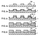
- An SR 4 plain laminate board was coated with Imagecure XV 501 at a dry film thickness of 25 microns.
- the board was imagewise exposed through a patterned mask so that the resist over the desired circuit patterned remained unharmed.
- the board was then developed in 0.6% by weight sodium carbonate solution [Fig.2(a)] and the resist layer remaining was then fully heat and UV cured.
- the board was then plasma etched and given an all-overcoat of metallic copper, 1 micron thick, by vacuum sputtering [Figure 2(b)].
- Another layer of resist was then deposited over the metal surface and photoimaged through the mask used to image the previous layer and this was then developed as before [Figure 2(c)].
- the board was then pattern electroplated and the resist stripped using 3% by weight sodium hydroxide solution [Figure 2(d)].
- the layer of vacuum deposited copper but not built up by the electroplating was then flash etched using acid ferric chloride solution.
- Example 1 The procedure of Example 1 was repeated up to the stage shown in Figure 1(b). A layer of copper (20 microns thick) was then electroplated over the surface of the thin layer of copper. [Figure 2(a)]. A layer of Imagecure XV 501 (about 25 microns dry thickness) was then deposited on to the board and photoimaged through a mask that was the negative of that used in the formation of the initial resist layer. This layer was developed as before [Figure 2(b)] and the copper exposed by this process was then etched away using acid ferric chloride etchant [Figure 2(c)]. The resist over the copper tracks remaining was then stripped away using 3% sodium hyroxide solution [Figure 2(d)].
Landscapes
- Engineering & Computer Science (AREA)
- Manufacturing & Machinery (AREA)
- Microelectronics & Electronic Packaging (AREA)
- Manufacturing Of Printed Circuit Boards (AREA)
- Production Of Multi-Layered Print Wiring Board (AREA)
Claims (1)
- Verfahren zur Herstellung einer mit Leiterbild eines elektrisch leitfähigen Metalls versehenen Isolierschicht auf einem Substrat, umfassend die Schritte der Erzeugung einer mit Leiterbild versehenen Reliefschicht eines elektrisch isolierenden Resist-Materials auf dem Substrat mit Hilfe eines Photo-Auflösungsprozesses, umfassend die Schritte:(i) Aufbringen einer Schicht eines strahlungshärtbaren Materials (2) auf das Substrat (1);(ii) bildpunktweises Exponieren der Schicht des strahlungshärtbaren Materials an Strahlung, um dadurch Abschnitte (2a) der an einer solchen Strahlung exponierten Schicht zu härten; und(iii) Entfernen der Abschnitte der nicht durch Strahlung exponierten Schicht (2b) mit Hilfe eines geeigneten Lösungsmittels, um dadurch auf dem Substrat eine mit Leiterbild versehene Schicht von gehärtetem strahlungshärtbarem Material (2a) zu erzeugen; sowienachfolgendes Einführen von elektrisch leitfähigem Metall in die Vertiefungen (Bahnen) in der mit Leiterbild versehenen Reliefschicht; bei welchem Verfahren das Metall in die Bahnen mit Hilfe der folgenden Schritte eingeführt wird:(iv) Aufbringen einer Schicht aus elektrisch leitfähigem Metall (4) über der Oberfläche des Substrats und des in Schritt (iii) des Photo-Auflösungsprozesses erhaltenen, mit Leiterbild versehenen und gehärteten Reliefmaterials; welche Methode gekennzeichnet ist durch die Schritte:(v) Aufbringen einer Schicht (5a, 5b) eines strahlungshärtbaren Materials (5) über der Oberfläche der in Schritt (iv) abgeschiedenen Metallschicht;(vi) bildpunktweises Exponieren der Schicht des strahlungshärtbaren Materials an Strahlung in einem zu dem in Schritt (ii) des Photo-Auflösungsprozesses negativen Leiterbildes, um dadurch Abschnitte (5b) des an einer solchen Strahlung exponierten strahlungshärtbaren Materials zu härten, jedoch in einem geringeren Maß als das mit Leiterbild versehene gehärtete Material (2a), das bereits auf dem Substrat vorhanden ist;(vii) Entfernen der nichtexponierten Abschnitte (5a) des strahlungshärtbaren Materials mit Hilfe eines geeigneten Lösungsmittels, um die in Schritt (iv) erhaltenen Abschnitte der Metallschicht (4) zu exponieren;(viii) Entfernen der Abschnitte des in Schritt (vii) exponierten Metalls, mit Hilfe eines geeigneten Ätzmittels;(ix) Entfernen des in Schritt (vi) erhaltenen gehärteten Materials (5b), um dadurch andere Abschnitte des in Schritt (iv) abgeschiedenen Metalls zu exponieren; sowie(x) Abscheiden von zusätzlichem, elektrisch leitfähigem Metall (4′) auf den mit Leiterbild versehenen Metallabschnitten, die in Schritt (ix) exponiert wurden.
Applications Claiming Priority (3)
| Application Number | Priority Date | Filing Date | Title |
|---|---|---|---|
| GB8908155 | 1989-04-11 | ||
| GB8908155A GB2230871A (en) | 1989-04-11 | 1989-04-11 | Making metal patterns. |
| PCT/GB1990/000562 WO1990012482A2 (en) | 1989-04-11 | 1990-04-11 | Printed circuit boards |
Publications (2)
| Publication Number | Publication Date |
|---|---|
| EP0467945A1 EP0467945A1 (de) | 1992-01-29 |
| EP0467945B1 true EP0467945B1 (de) | 1995-10-25 |
Family
ID=10654818
Family Applications (1)
| Application Number | Title | Priority Date | Filing Date |
|---|---|---|---|
| EP90906316A Expired - Lifetime EP0467945B1 (de) | 1989-04-11 | 1990-04-11 | Gedruckte schaltungsplatten |
Country Status (4)
| Country | Link |
|---|---|
| EP (1) | EP0467945B1 (de) |
| DE (1) | DE69023234T2 (de) |
| GB (1) | GB2230871A (de) |
| WO (1) | WO1990012482A2 (de) |
Families Citing this family (6)
| Publication number | Priority date | Publication date | Assignee | Title |
|---|---|---|---|---|
| US5322763A (en) * | 1992-05-06 | 1994-06-21 | E. I. Du Pont De Nemours And Company | Process for making metal ledge on stencil screen |
| US5573815A (en) * | 1994-03-07 | 1996-11-12 | E. I. Du Pont De Nemours And Company | Process for making improved metal stencil screens for screen printing |
| TW277204B (de) * | 1994-12-02 | 1996-06-01 | Nippon Paint Co Ltd | |
| GB9606497D0 (en) * | 1996-03-27 | 1996-06-05 | Coates Brothers Plc | Production of electrical circuit boards |
| CN110058490A (zh) * | 2011-08-10 | 2019-07-26 | 日立化成株式会社 | 感光性树脂组合物、感光性薄膜、永久抗蚀剂以及永久抗蚀剂的制造方法 |
| EP4374420A4 (de) * | 2021-07-20 | 2025-06-04 | Entegris, Inc. | Verfahren zum aufbringen einer deckenden polymerbeschichtung auf ein substrat |
Family Cites Families (12)
| Publication number | Priority date | Publication date | Assignee | Title |
|---|---|---|---|---|
| GB585035A (en) * | 1944-03-27 | 1947-01-29 | Kodak Ltd | Improvements in the production of articles comprising metal |
| DE1267738B (de) * | 1962-10-29 | 1968-05-09 | Intellux Inc | Verfahren zur Herstellung von elektrischen Verbindungen zwischen den Stromkreisen von mehrlagigen gedruckten elektrischen Schaltungen |
| DE2658400A1 (de) * | 1976-12-23 | 1978-06-29 | Ibm Deutschland | Verfahren zur herstellung einer negativen maske auf einem substrat |
| US4307179A (en) * | 1980-07-03 | 1981-12-22 | International Business Machines Corporation | Planar metal interconnection system and process |
| US4576900A (en) * | 1981-10-09 | 1986-03-18 | Amdahl Corporation | Integrated circuit multilevel interconnect system and method |
| JPS5986045A (ja) * | 1982-11-05 | 1984-05-18 | Nippon Soda Co Ltd | 永久レジスト用光硬化性樹脂組成物 |
| US4645733A (en) * | 1983-11-10 | 1987-02-24 | Sullivan Donald F | High resolution printed circuits formed in photopolymer pattern indentations overlaying printed wiring board substrates |
| US4775611A (en) * | 1983-11-10 | 1988-10-04 | Sullivan Donald F | Additive printed circuit boards with flat surface and indented primary wiring conductors |
| US4525448A (en) * | 1984-01-06 | 1985-06-25 | International Telephone And Telegraph Corporation | Method of fabricating sub-half-micron-size gates on semiconductor substrates |
| US4567132A (en) * | 1984-03-16 | 1986-01-28 | International Business Machines Corporation | Multi-level resist image reversal lithography process |
| DE3881911D1 (de) * | 1987-03-09 | 1993-07-29 | Siemens Nixdorf Inf Syst | Aufbautechnik fuer mehrlagige verdrahtungen. |
| US4921777A (en) * | 1987-08-03 | 1990-05-01 | Allied-Signal Inc. | Method for manufacture of multilayer printed circuit boards |
-
1989
- 1989-04-11 GB GB8908155A patent/GB2230871A/en not_active Withdrawn
-
1990
- 1990-04-11 EP EP90906316A patent/EP0467945B1/de not_active Expired - Lifetime
- 1990-04-11 DE DE69023234T patent/DE69023234T2/de not_active Expired - Fee Related
- 1990-04-11 WO PCT/GB1990/000562 patent/WO1990012482A2/en not_active Ceased
Also Published As
| Publication number | Publication date |
|---|---|
| DE69023234T2 (de) | 1996-05-02 |
| WO1990012482A3 (en) | 1990-12-27 |
| DE69023234D1 (de) | 1995-11-30 |
| WO1990012482A2 (en) | 1990-10-18 |
| GB8908155D0 (en) | 1989-05-24 |
| EP0467945A1 (de) | 1992-01-29 |
| GB2230871A (en) | 1990-10-31 |
Similar Documents
| Publication | Publication Date | Title |
|---|---|---|
| EP0526243B1 (de) | Via-Loch Struktur und Verfahren | |
| US6368697B1 (en) | Method of manufacturing an interlayer via and a laminate precursor useful for same | |
| CA2345829C (en) | Process to manufacture tight tolerance embedded elements for printed circuit boards | |
| JP2001509966A (ja) | 高密度多層相互連結印刷回路基板の作製 | |
| US5763140A (en) | Photodefinable dielectric composition useful in the manufacture of printed circuits | |
| EP0096701B1 (de) | Zu vergrössertem aufnahmevermögen führende leiterplattenherstellung | |
| EP2496062A1 (de) | Verfahren zur Ausbildung von festen Blinddurchgängen durch den dielektrischen Überzug auf Substratmaterialien hochintegrierter Schaltungen (HDI) | |
| EP0257737A2 (de) | Gedruckte Schaltungsvorläufer | |
| WO1990012482A2 (en) | Printed circuit boards | |
| EP0867106A2 (de) | Lötstopmaske zur herstellung gedruckter schaltungen | |
| US6739048B2 (en) | Process of fabricating a circuitized structure | |
| EP0360744B1 (de) | Verfahren zur Herstellung elektrisch leitfähiger Muster | |
| JP2778323B2 (ja) | プリント配線基板およびその製造方法 | |
| WO1989007785A1 (en) | Coating compositions | |
| GB2299585A (en) | Coating compositions | |
| JPH06260763A (ja) | 多層配線基板の製造方法 | |
| JP3593351B2 (ja) | 多層配線基板の製造方法 | |
| JPS63310196A (ja) | 金属パターンの形成方法 | |
| JPS61279198A (ja) | プリント回路の製造方法 | |
| WO1997036464A1 (en) | Production of electrical circuit boards | |
| JPWO2000052977A1 (ja) | 多層配線基板の製造方法 | |
| JPH01189993A (ja) | プリント配線板の製造方法 | |
| JPH1140945A (ja) | 多層プリント配線板の製造方法 | |
| JPH0737277A (ja) | マスター基板 | |
| JPH02143584A (ja) | スルーホール付配線板の製造方法 |
Legal Events
| Date | Code | Title | Description |
|---|---|---|---|
| PUAI | Public reference made under article 153(3) epc to a published international application that has entered the european phase |
Free format text: ORIGINAL CODE: 0009012 |
|
| 17P | Request for examination filed |
Effective date: 19911004 |
|
| AK | Designated contracting states |
Kind code of ref document: A1 Designated state(s): DE FR GB IT SE |
|
| 17Q | First examination report despatched |
Effective date: 19930428 |
|
| GRAA | (expected) grant |
Free format text: ORIGINAL CODE: 0009210 |
|
| AK | Designated contracting states |
Kind code of ref document: B1 Designated state(s): DE FR GB IT SE |
|
| ITF | It: translation for a ep patent filed | ||
| REF | Corresponds to: |
Ref document number: 69023234 Country of ref document: DE Date of ref document: 19951130 |
|
| ET | Fr: translation filed | ||
| PLBE | No opposition filed within time limit |
Free format text: ORIGINAL CODE: 0009261 |
|
| STAA | Information on the status of an ep patent application or granted ep patent |
Free format text: STATUS: NO OPPOSITION FILED WITHIN TIME LIMIT |
|
| 26N | No opposition filed | ||
| REG | Reference to a national code |
Ref country code: GB Ref legal event code: IF02 |
|
| PGFP | Annual fee paid to national office [announced via postgrant information from national office to epo] |
Ref country code: SE Payment date: 20050406 Year of fee payment: 16 Ref country code: GB Payment date: 20050406 Year of fee payment: 16 |
|
| PGFP | Annual fee paid to national office [announced via postgrant information from national office to epo] |
Ref country code: DE Payment date: 20050407 Year of fee payment: 16 |
|
| PGFP | Annual fee paid to national office [announced via postgrant information from national office to epo] |
Ref country code: FR Payment date: 20050408 Year of fee payment: 16 |
|
| PG25 | Lapsed in a contracting state [announced via postgrant information from national office to epo] |
Ref country code: GB Free format text: LAPSE BECAUSE OF NON-PAYMENT OF DUE FEES Effective date: 20060411 |
|
| PG25 | Lapsed in a contracting state [announced via postgrant information from national office to epo] |
Ref country code: SE Free format text: LAPSE BECAUSE OF NON-PAYMENT OF DUE FEES Effective date: 20060412 |
|
| PGFP | Annual fee paid to national office [announced via postgrant information from national office to epo] |
Ref country code: IT Payment date: 20060430 Year of fee payment: 17 |
|
| PG25 | Lapsed in a contracting state [announced via postgrant information from national office to epo] |
Ref country code: DE Free format text: LAPSE BECAUSE OF NON-PAYMENT OF DUE FEES Effective date: 20061101 |
|
| EUG | Se: european patent has lapsed | ||
| GBPC | Gb: european patent ceased through non-payment of renewal fee |
Effective date: 20060411 |
|
| REG | Reference to a national code |
Ref country code: FR Ref legal event code: ST Effective date: 20061230 |
|
| PG25 | Lapsed in a contracting state [announced via postgrant information from national office to epo] |
Ref country code: FR Free format text: LAPSE BECAUSE OF NON-PAYMENT OF DUE FEES Effective date: 20060502 |
|
| PG25 | Lapsed in a contracting state [announced via postgrant information from national office to epo] |
Ref country code: IT Free format text: LAPSE BECAUSE OF NON-PAYMENT OF DUE FEES Effective date: 20070411 |