EP0457522B1 - Circuits de correction de gamma - Google Patents
Circuits de correction de gamma Download PDFInfo
- Publication number
- EP0457522B1 EP0457522B1 EP91304259A EP91304259A EP0457522B1 EP 0457522 B1 EP0457522 B1 EP 0457522B1 EP 91304259 A EP91304259 A EP 91304259A EP 91304259 A EP91304259 A EP 91304259A EP 0457522 B1 EP0457522 B1 EP 0457522B1
- Authority
- EP
- European Patent Office
- Prior art keywords
- video signal
- data
- circuit
- digital video
- gamma correction
- Prior art date
- Legal status (The legal status is an assumption and is not a legal conclusion. Google has not performed a legal analysis and makes no representation as to the accuracy of the status listed.)
- Expired - Lifetime
Links
- 238000012937 correction Methods 0.000 title claims description 74
- 238000013459 approach Methods 0.000 description 3
- 238000010586 diagram Methods 0.000 description 3
- 238000012545 processing Methods 0.000 description 3
- 238000006243 chemical reaction Methods 0.000 description 2
- 238000013507 mapping Methods 0.000 description 2
- 238000000034 method Methods 0.000 description 2
- 241000270295 Serpentes Species 0.000 description 1
Images


Classifications
-
- H—ELECTRICITY
- H04—ELECTRIC COMMUNICATION TECHNIQUE
- H04N—PICTORIAL COMMUNICATION, e.g. TELEVISION
- H04N5/00—Details of television systems
- H04N5/14—Picture signal circuitry for video frequency region
- H04N5/20—Circuitry for controlling amplitude response
- H04N5/202—Gamma control
-
- H—ELECTRICITY
- H04—ELECTRIC COMMUNICATION TECHNIQUE
- H04N—PICTORIAL COMMUNICATION, e.g. TELEVISION
- H04N23/00—Cameras or camera modules comprising electronic image sensors; Control thereof
- H04N23/80—Camera processing pipelines; Components thereof
- H04N23/82—Camera processing pipelines; Components thereof for controlling camera response irrespective of the scene brightness, e.g. gamma correction
Definitions
- This invention relates to gamma correction circuits.
- the relationship between a grid signal voltage and a luminous output of a colour image receiving tube is not linear.
- the luminous output is proportional to, for example, 2.2-th power of an input signal applied to the grid.
- a signal from a video camera is applied to a colour image receiving tube without prior treatment, not only the luminance of an image on the screen, but also the hue and/or saturation, vary to a large degree.
- the input signal is passed through a gamma correction circuit having an input/output characteristic such that the output signal is equal to, for example, the 2.2-th power of the input signal, thereby to provide that the overall characteristic is linear.
- Such a gamma correction circuit It is possible to position such a gamma correction circuit to process the signal immediately before it is applied to the grid of the colour image receiving tube.
- a gamma correction circuit is generally not provided in association with a colour image receiver of a domestic electric apparatus. Instead, it is provided on the transmitting side, generally in a video camera.
- mapping system in which a gamma correction characteristic prepared in advance is stored in memory and a gamma corrected digital video signal is read from the memory. More specifically, an output signal level of the input/output characteristic for the gamma correction is stored in advance in the memory and an output signal level is read from the memory by using an input signal level as a readout address for the memory to provide a gamma corrected output signal.
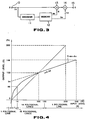
- a gamma correction circuit designed to perform gamma correction using a polygonal line approximating to a desired gamma correction characteristic. More specifically, as shown in Figure 2, an approach is used in which characteristics of respective lines (line segments or portions) forming an approximation to a polygonal line are realised in respective operation circuits l1 to l n comprising multiplier circuits and adder circuits, etc., and outputs from the respective operation circuits l1 to l n are compared with each other in a comparison circuit (comparator) 2 to select the minimum value, thereby to provide a gamma corrected digital video signal.
- a memory of larger capacity is required.
- the increased memory capacity is an obstruction.
- the memory configuration generally employed is a configuration in which 8 bits are taken as one byte for carrying out writing and reading of bytes of data. Accordingly, if the number of bits per sample of a digital video signal is greater than 8, the use efficiency of the memory is poor.
- a gamma correction circuit according to the pre-characterising part of claim 1 hereof for a digital video signal, the circuit being characterised in that:
- the gamma correction circuit enables a desired gamma correction of a digital video signal to be carried out by using slope data and intercept data of respective line segments or portions read out from the memory means, and allows the gamma correction characteristic to be changed by multiplying the level data read out from the memory means by different suitable coefficient data.
- a preferred embodiment of the invention described in detail hereinbelow provides a gamma correction circuit which permits the memory capacity to be smaller than that of the prior proposal described above, in carrying out gamma correction of a digital video signal by using a polygonal line approximating to a desired gamma correction characteristic, and thus permits the entire circuit scale to be smaller. Also, the preferred embodiment permits changing of the gamma correction characteristic with a circuit scale smaller than that of the prior proposal described above.
- FIG 3 shows the configuration of a gamma correction circuit.
- a digital video signal X provided by converting a video signal from a charge coupled device (CCD) image sensor (hereinafter referred to as a CCD) of, for example, a video camera to a digital signal is supplied to an encoder 11 and to a multiplier circuit 13 from an input terminal 10.
- CCD charge coupled device
- the encoder 11 converts the input digital video signal X to a readout address for a memory circuit 12.
- the memory circuit 12 comprises, for example, a random access memory (RAM).
- RAM random access memory
- slopes hereinafter referred to as slope data a n
- intercepts hereinafter referred to as intercept data b n
- the slope data a n and the intercept data b n stored in the memory circuit 12 are read out on the basis of a readout address from the encoder 11.
- the slope data a n thus read out are supplied to the multiplier circuit 13, and the intercept data b n thus read out are supplied to an adder circuit 14.
- the multiplier circuit 13 multiplies the input digital video signal X supplied via the input terminal 10 by slope data a n from the memory circuit 12 and supplies the multiplied result (product) to the adder circuit 14.
- the adder circuit 14 adds the output from the multiplier circuit 13 and intercept data b n from the memory circuit 12 to output the added result (sum), at an output terminal 15, as a gamma corrected digital video signal Y.
- the memory circuit 12 is used as memory means for storing slope data and intercept data of respective line segments
- the encoder 11 is used as address conversion means for converting a level of an input signal to a readout address for the memory circuit 12
- the multiplier circuit 13 is used as multiplier means for multiplying slope data a n , read out from the memory circuit 12 on the basis of an address from the encoder 11, by an input signal
- the adder circuit 14 is used as adder means for adding intercept data b n , read out from the memory circuit 12 on the basis of an address from the encoder 11, and the multiplied value (product) from the multiplier circuit 13.
- the memory circuit 12 stores, as mentioned above, slope data an and intercept data b n of respective line segments of a polygonal line approximating to the gamma correction characteristic.
- the gamma correction characteristic is approximated by 1 polygonal line; when that signal X is 0 to 15%, corresponding to the black area where an output signal varies to a large degree, the gamma correction characteristic is approximated by 16 polygonal lines; when that signal X is 15 to 120%, the gamma correction characteristic is approximated by 14 polygonal lines; and when that signal X is more than 120%, the gamma correction characteristic is approximated by 1 polygonal line.
- slope data a n (assumed to comprise, for example, 8 bits) and intercept data b n (assumed to comprise, for example, 12 bits) are stored in the memory circuit 12.
- the encoder 11 converts the input digital video signal X supplied via the input terminal 10 to a readout address for the memory circuit 12.
- the input digital video signal X when the input digital video signal X is less than 0% of the reference white level, the input digital video signal X of, for example, 14 bits is converted to one address; when that signal X is 0 to 15%, the input digital video signal X is converted to 16 addresses; when that signal X is 15 to 120%, the input digital video signal X is converted to 14 addresses; and when that signal X is more than 120%, the input digital video signal X is converted to one address.
- the input digital video signal X of 14 bits is converted to a readout address of 5 bits in correspondence with the 32 polygonal line approximation. Then, slope data a n and intercept data b n read out by using this readout address are supplied to the multiplier circuit 13 and the adder circuit 14, respectively.
- the multiplier circuit 13 multiplies the input digital video signal X by the slope data a n , and the adder circuit 14 adds the output from the multiplier circuit 13 and the intercept data b n .
- slope data a n and intercept data b n of respective line segments of a polygonal line approximating to a desired gamma correction characteristic are written in advance into the memory circuit 12.
- the input digital video signal X is converted to a readout address for the memory circuit 12 so that slope data a n and intercept data b n are read out from the memory circuit 12 on the basis of the readout address so that the operation expressed by Equation (1) above is performed by the multiplier circuit 13 and the adder circuit 14, thereby providing a gamma corrected digital video signal.
- the capacity of the memory circuit 12 can be reduced.
- the operation circuit can be constituted by the single multiplier circuit 13 and the single adder circuit 14.
- the gamma correction circuit can be realised on a circuit scale smaller than that of the previous proposal described above with reference to Figure 2.
- a gamma correction circuit according to an embodiment of this invention is shown in Figure 5.
- an input digital video signal X is supplied to an encoder 21, and to adder circuits 23 and 27, from an input terminal 20.
- the encoder 21 converts the input digital video signal X to a readout address for a memory circuit 22 in the same manner as in the circuit of Figure 3.
- the memory circuit 22 may, for example, comprise a RAM.
- the slope data a m , the intercept data b m , and the bend point data X m stored in the memory circuit 22 are read out on the basis of the readout address from the encoder 21.
- the bend point data X m thus read out are supplied to a subtraction terminal of the adder circuit 23, the slope data a m thus read out are supplied to a multiplier circuit 24, and the intercept data b m are supplied to an adder circuit 25.
- the adder circuit 23 subtracts the bend point data X m from the input digital video signal X supplied from the input terminal 20 and supplies the subtracted result to the multiplier circuit 24.
- the multiplier circuit 24 multiplies an output from the adder circuit 23 by slope data a m from the memory circuit 22 and supplies the multiplied result (product) to the adder circuit 25.
- the adder circuit 25 adds an output from the multiplier circuit 24 and intercept data b m from the memory circuit 22 and supplies the added result (sum) to a multiplier circuit 26.
- the multiplier circuit 26 multiplies an output from the adder circuit 25 by a coefficient K for altering the gamma correction characteristic and supplies the multiplied result (product) to the adder circuit 27.
- the coefficient K is supplied to the multiplier circuit 28 via a terminal 28.
- the adder circuit 27 adds an output from the multiplier circuit 26 and the input digital video signal X to output, at an output terminal 29, the added result (sum) as a gamma corrected digital video signal Z.
- the above-mentioned curve is approximated by 1 polygonal line; when that signal X is 0 to 15%, the above-mentioned curve is approximated by 16 polygonal lines; when that signal X is 15 to 120%, the above-mentioned curve is approximated by 14 polygonal lines; and when that signal X is more than 120%, the above-mentioned curve signal is approximated by 1 polygonal line.
- slope data a m of respective line segments or portions of 32 polygonal lines and assumed to comprise 8 bits, bend point data X m assumed to comprise 14 bits, and intercept data b m at respective levels X m assumed to comprise 11 bits, are stored in the memory circuit 22.
- the encoder 21 converts an input digital video signal X to a readout address for the memory circuit 22.
- an input digital video signal X of, for example, 14 bits is converted to a readout address of 5 bits in correspondence with the 32 polygonal approximation in the same manner as in the circuit of Figure 3.
- bend point data X m read out by using this readout address are supplied to the adder circuit 23
- the slope data a m similarly ready out are supplied to the multiplier circuit 24
- the intercept data b m similarly read out are supplied to the adder circuit 25.
- the adder circuit 23 subtracts the bend point data X m from the input digital video signal X, the multiplier circuit 24 multiplies an output from the adder circuit 23 by the slope data a m , the adder circuit 25 adds an output from the multiplier circuit 24 to the intercept data b m , the multiplier circuit 26 multiplies an output from the adder circuit 25 by the coefficient K supplied via the terminal 28, and the adder circuit 27 adds an output from the multiplier circuit 26 to the input digital video signal X.
- Equation (2) At the points where the input digital video signal X is 0% and 100%, the value of the first term of Equation (2) becomes equal to zero.
- the coefficient K it is possible to vary the curve of the gamma correction characteristic without changing the gamma correction characteristic at the points where the input digital video signal X is 0% and 100%.
- the input digital video signal X is converted to a readout address for the memory circuit 22 so that the slope data a m , the intercept data b m , and the bend point data X m are read out from the memory circuit 22 on the basis of this readout address so that the operation expressed by Equation (2) is carried out by the circuits 23 to 27, thereby providing a gamma corrected digital video signal Z.
- the operation circuit can be constituted by the two multiplier circuits 24 and 26 and the three adder circuits 23, 25 and 27.
- the gamma correction circuit can be constituted on a circuit scale smaller than that of the prior proposal described above.
- the gamma correction characteristic can be altered by altering the coefficient K supplied via the terminal 28.
- the number of bits multiplied at the multiplier circuit 24 can be smaller than that of the embodiment of Figure 3.
- the maximum value of the intercept data b m of this embodiment is smaller than the maximum value of the intercept data b n of the circuit of Figure 3, the number of bits can be smaller than that of the circuit of Figure 3.
- the gamma correction circuit employs an approach of storing advance slope data and intercept data of respective line segments of a polygonal line approximating a desired gamma correction characteristic in a memory means, converting a level of an input signal to a readout address for the memory means in address conversion means, and reading out the slope data and intercept data from the memory means on the basis of this readout address to perform a processing operation at multiplier means and adder means, thereby to provide a gamma corrected digital video signal.
- the circuitry for carrying out the above-mentioned operation can be simply constituted.
- the gamma correction circuit can be realised on a circuit scale smaller than that of the prior proposal described above.
- the number of line segments forming a polygonal line can be larger than that of the prior proposal, so that it is possible for the precision of the approximation to be high.
- by changing values of the slope data and the intercept data stored into the memory means it is possible to readily cope with diverse gamma correction characteristics, for example in dependence upon broadcasting stations.
Landscapes
- Engineering & Computer Science (AREA)
- Multimedia (AREA)
- Signal Processing (AREA)
- Picture Signal Circuits (AREA)
- Processing Of Color Television Signals (AREA)
Claims (3)
- Circuit de correction de gamma pour un signal vidéo numérique, le circuit comprenant:- des moyens de mémoire (22) pour mémoriser des données de pente et des données d'intersection de chaque partie d'une pluralité de parties d'une ligne polygonale approximant une caractéristique désirée de correction de gamma;- des moyens de conversion (21) pour convertir le signal vidéo numérique en données d'adresse pour les moyens de mémoire (22);- des moyens de multiplication (34) pour multiplier les données de pente lues dans les moyens de mémoire (22) selon lesdites données d'adresse lues, par le signal vidéo numérique; et- des moyens d'addition (25) pour additionner les données d'intersection lues dans les moyens de mémoire (22) selon lesdites données d'adresse lues et un signal de sortie issu des moyens de multiplication (24) pour fournir un signal de sortie corrigé en gamma à partir de ceux-ci,le circuit de correction de gamma étant caractérisé en ce que:- les données de pente, les données d'intersection et les données de points d'inflexion des segments de droite respectifs d'une ligne polygonale approximant une courbe de correction obtenue en soustrayant le niveau d'un signal vidéo qui n'est pas encore corrigé en gamma de ladite caractéristique de correction de gamma, sont mémorisées dans les moyens de mémoire (22);- des moyens de soustraction (23) sont prévus pour soustraire dudit signal vidéo numérique les données de points d'inflexion lues dans les moyens de mémoire (22) selon lesdites données d'adresse lues, et fournir le signal de sortie soustrait aux moyens de multiplication (24);- des deuxième moyens d'addition (27) sont prévus pour additionner le signal de sortie des premiers moyens d'addition (25) et ledit signal vidéo numérique pour fournir un signal vidéo numérique corrigé en gamma; et- des deuxièmes moyens de multiplication (26) sont prévus pour multiplier le signal de sortie des premiers moyens d'addition (25) par un coefficient (K) et fournir le signal de sortie multiplié aux deuxièmes moyens d'addition (27).
- Circuit de correction de gamma selon la revendication 1, dans lequel les moyens de mémoire (22) mémorisent les données de pente, les données d'intersection et les données de points d'inflexion de 32 segments d'une ligne polygonale, le circuit fonctionnant de telle manière que l'approximation par lesdits 32 segments d'une ligne polygonale est effectuée de telle manière que la courbe de correction pour un signal vidéo d'entrée de moins de 0% par rapport au niveau de référence du blanc est approximée par un segment de la ligne polygonale, la courbe de correction pour un signal vidéo d'entrée de 0 à 15% par rapport audit niveau de référence du blanc est approximée par 16 segments de la ligne polygonale, la courbe de correction pour un signal vidéo d'entrée de 15 à 120% par rapport audit niveau de référence du blanc est approximée par 14 segments de la ligne polygonale; et la courbe de correction pour un signal vidéo d'entrée de plus de 120% par rapport audit niveau de référence du blanc est approximée par un segment de la ligne polygonale.
- Circuit de correction de gamma selon la revendication 1 ou la revendication 2, qui est incorporé à une caméra vidéo numérique ayant des moyens capteurs d'images pour produire un signal vidéo correspondant à une image d'un objet, et des moyens de convertisseur analogique/numérique pour convertir le signal vidéo produit en ledit signal vidéo numérique.
Applications Claiming Priority (2)
| Application Number | Priority Date | Filing Date | Title |
|---|---|---|---|
| JP2121236A JP2924079B2 (ja) | 1990-05-14 | 1990-05-14 | ガンマ補正回路 |
| JP121236/90 | 1990-05-14 |
Publications (3)
| Publication Number | Publication Date |
|---|---|
| EP0457522A2 EP0457522A2 (fr) | 1991-11-21 |
| EP0457522A3 EP0457522A3 (en) | 1992-07-01 |
| EP0457522B1 true EP0457522B1 (fr) | 1996-03-06 |
Family
ID=14806284
Family Applications (1)
| Application Number | Title | Priority Date | Filing Date |
|---|---|---|---|
| EP91304259A Expired - Lifetime EP0457522B1 (fr) | 1990-05-14 | 1991-05-13 | Circuits de correction de gamma |
Country Status (5)
| Country | Link |
|---|---|
| US (1) | US5243426A (fr) |
| EP (1) | EP0457522B1 (fr) |
| JP (1) | JP2924079B2 (fr) |
| KR (1) | KR100215150B1 (fr) |
| DE (1) | DE69117579T2 (fr) |
Cited By (2)
| Publication number | Priority date | Publication date | Assignee | Title |
|---|---|---|---|---|
| US7038721B2 (en) | 2002-02-15 | 2006-05-02 | Koninklijke Philips Electronics N.V. | Gamma correction circuit |
| US8614719B2 (en) | 2006-07-12 | 2013-12-24 | Freescale Semiconductor, Inc. | Method for gamma correction and a device having gamma correction capabilities |
Families Citing this family (18)
| Publication number | Priority date | Publication date | Assignee | Title |
|---|---|---|---|---|
| GB2258782B (en) * | 1991-07-30 | 1995-04-12 | Samsung Electronics Co Ltd | Method and apparatus for gamma correction |
| KR950005050Y1 (ko) * | 1991-12-05 | 1995-06-21 | 삼성전자 주식회사 | 디지탈 카메라의 아날로그 겸용회로 |
| JP2989953B2 (ja) * | 1992-02-10 | 1999-12-13 | 富士ゼロックス株式会社 | 定着装置及び定着用エンドレスベルト |
| JP3302423B2 (ja) * | 1992-12-28 | 2002-07-15 | キヤノン株式会社 | 撮像装置 |
| US5473373A (en) * | 1994-06-07 | 1995-12-05 | Industrial Technology Research Institute | Digital gamma correction system for low, medium and high intensity video signals, with linear and non-linear correction |
| KR960024524A (ko) * | 1994-12-21 | 1996-07-20 | 김광호 | 기억소자를 이용한 액정 표시장치의 감마 보정장치 |
| US5539459A (en) * | 1995-05-18 | 1996-07-23 | Polaroid Corporation | Optimal tone scale mapping in electronic cameras |
| JPH0946554A (ja) * | 1995-07-31 | 1997-02-14 | Sony Corp | 撮像装置 |
| GB2305571B8 (en) * | 1995-09-22 | 2000-01-31 | Ibm | Display apparatus with gamma correction |
| KR100342964B1 (ko) | 1998-10-06 | 2002-07-05 | 마츠시타 덴끼 산교 가부시키가이샤 | 감마 보정 회로 및 감마 보정 방법 |
| US6137542A (en) * | 1998-12-21 | 2000-10-24 | Phillips Electronics North America Corporation | Digital correction of linear approximation of gamma |
| US6791576B1 (en) | 2000-02-23 | 2004-09-14 | Neomagic Corp. | Gamma correction using double mapping with ratiometrically-related segments of two different ratios |
| US7042523B2 (en) * | 2003-06-30 | 2006-05-09 | Texas Instruments Incorporated | Video correction system and method using logarithmic conversion |
| US7154562B1 (en) | 2003-10-14 | 2006-12-26 | Cirrus Logic, Inc. | Methods and circuits for implementing programmable gamma correction |
| JP4255467B2 (ja) * | 2005-10-26 | 2009-04-15 | シャープ株式会社 | デジタルガンマ補正回路およびデジタルガンマ補正方法 |
| JP4330596B2 (ja) * | 2006-03-31 | 2009-09-16 | シャープ株式会社 | デジタルガンマ補正回路およびデジタルガンマ補正方法 |
| JP5541938B2 (ja) * | 2010-02-01 | 2014-07-09 | オリンパスイメージング株式会社 | 撮影装置 |
| US8817173B2 (en) * | 2010-02-01 | 2014-08-26 | Olympus Imaging Corp. | Photographing apparatus capable of flash emission |
Family Cites Families (11)
| Publication number | Priority date | Publication date | Assignee | Title |
|---|---|---|---|---|
| US4187519A (en) * | 1978-08-17 | 1980-02-05 | Rockwell International Corporation | System for expanding the video contrast of an image |
| JPS57204931A (en) * | 1981-06-12 | 1982-12-15 | Nec Corp | Nonlinear converter |
| US4805013A (en) * | 1984-09-05 | 1989-02-14 | Canon Kabushiki Kaisha | Image data conversion system |
| JPS6260392A (ja) * | 1985-09-10 | 1987-03-17 | Mitsubishi Electric Corp | 逆ガンマ補正回路 |
| JPS63120564A (ja) * | 1986-11-10 | 1988-05-24 | Matsushita Electric Ind Co Ltd | テレビジヨンカメラのガンマ補正回路 |
| JP2521183Y2 (ja) * | 1987-09-29 | 1996-12-25 | ソニー株式会社 | ディジタル信号処理回路 |
| JPH07122369B2 (ja) * | 1988-07-21 | 1995-12-25 | アイシン精機株式会社 | ドアロツク装置 |
| US5089890A (en) * | 1989-02-06 | 1992-02-18 | Canon Kabushiki Kaisha | Gamma correction device |
| US4975773A (en) * | 1989-03-31 | 1990-12-04 | Zenith Electronics Corporation | Dynamic range video black level expander |
| US5258928A (en) * | 1990-05-03 | 1993-11-02 | Rca Thomson Licensing Corporation | Parts efficient memory based functional circuit having selectable transfer characteristics |
| US5047861A (en) * | 1990-07-31 | 1991-09-10 | Eastman Kodak Company | Method and apparatus for pixel non-uniformity correction |
-
1990
- 1990-05-14 JP JP2121236A patent/JP2924079B2/ja not_active Expired - Lifetime
-
1991
- 1991-04-29 US US07/693,007 patent/US5243426A/en not_active Expired - Lifetime
- 1991-05-10 KR KR1019910007526A patent/KR100215150B1/ko not_active IP Right Cessation
- 1991-05-13 DE DE69117579T patent/DE69117579T2/de not_active Expired - Lifetime
- 1991-05-13 EP EP91304259A patent/EP0457522B1/fr not_active Expired - Lifetime
Cited By (2)
| Publication number | Priority date | Publication date | Assignee | Title |
|---|---|---|---|---|
| US7038721B2 (en) | 2002-02-15 | 2006-05-02 | Koninklijke Philips Electronics N.V. | Gamma correction circuit |
| US8614719B2 (en) | 2006-07-12 | 2013-12-24 | Freescale Semiconductor, Inc. | Method for gamma correction and a device having gamma correction capabilities |
Also Published As
| Publication number | Publication date |
|---|---|
| KR910021117A (ko) | 1991-12-20 |
| JP2924079B2 (ja) | 1999-07-26 |
| DE69117579T2 (de) | 1996-08-08 |
| EP0457522A3 (en) | 1992-07-01 |
| DE69117579D1 (de) | 1996-04-11 |
| EP0457522A2 (fr) | 1991-11-21 |
| KR100215150B1 (ko) | 1999-08-16 |
| JPH0418865A (ja) | 1992-01-23 |
| US5243426A (en) | 1993-09-07 |
Similar Documents
| Publication | Publication Date | Title |
|---|---|---|
| EP0457522B1 (fr) | Circuits de correction de gamma | |
| US7352398B2 (en) | Image pick-up apparatus and method for picking up and synthesizing plural images to generate a dynamic range image | |
| US5784100A (en) | Apparatus and method for performing shading correction by multiplying a differential shading correction factor and input image data | |
| JP2549753B2 (ja) | ガンマ補正回路および方法 | |
| EP0309149B1 (fr) | Traitement d'images | |
| EP0957628A2 (fr) | Appareil de lecture d'images et support d'enregistrement lisible par ordinateur | |
| CA2063472A1 (fr) | Methode de conversion de definition | |
| CA2036100C (fr) | Appareil corrigeant la gradation de l'image transmise | |
| CA2085754C (fr) | Dispositif de correction de la luminance d'images video | |
| US7317482B2 (en) | Distance calculating method and imaging device | |
| JP3031994B2 (ja) | 画像処理装置 | |
| EP0532295A2 (fr) | Circuit de correction de l'échelle des gris | |
| US5940146A (en) | Video apparatus with image memory function | |
| KR960014313B1 (ko) | 화상신호처리장치 | |
| US7626623B2 (en) | Signal processing apparatus, signal processing method, program, and storage medium employing random number generation | |
| US5905533A (en) | Image processing apparatus | |
| JP3045245B2 (ja) | ガンマ補正回路 | |
| EP0604759B1 (fr) | Procédé et appareil pour traiter des données digitales d'image | |
| JPS6135751B2 (fr) | ||
| JP2001086365A (ja) | ガンマ補正回路およびニー補正回路 | |
| EP0542267B1 (fr) | Circuit de correction par dispositif d'analyse d'image | |
| US6806916B1 (en) | Video apparatus with image memory function | |
| JPH0646771B2 (ja) | カラー画像入力表示装置 | |
| JP3577525B2 (ja) | 電子カメラ | |
| JPH04217173A (ja) | 画像データ変換方法及び画像データ変換装置 |
Legal Events
| Date | Code | Title | Description |
|---|---|---|---|
| PUAI | Public reference made under article 153(3) epc to a published international application that has entered the european phase |
Free format text: ORIGINAL CODE: 0009012 |
|
| AK | Designated contracting states |
Kind code of ref document: A2 Designated state(s): DE FR GB |
|
| PUAL | Search report despatched |
Free format text: ORIGINAL CODE: 0009013 |
|
| AK | Designated contracting states |
Kind code of ref document: A3 Designated state(s): DE FR GB |
|
| 17P | Request for examination filed |
Effective date: 19921112 |
|
| 17Q | First examination report despatched |
Effective date: 19940901 |
|
| GRAA | (expected) grant |
Free format text: ORIGINAL CODE: 0009210 |
|
| AK | Designated contracting states |
Kind code of ref document: B1 Designated state(s): DE FR GB |
|
| REF | Corresponds to: |
Ref document number: 69117579 Country of ref document: DE Date of ref document: 19960411 |
|
| ET | Fr: translation filed | ||
| PLBE | No opposition filed within time limit |
Free format text: ORIGINAL CODE: 0009261 |
|
| STAA | Information on the status of an ep patent application or granted ep patent |
Free format text: STATUS: NO OPPOSITION FILED WITHIN TIME LIMIT |
|
| 26N | No opposition filed | ||
| REG | Reference to a national code |
Ref country code: GB Ref legal event code: IF02 |
|
| PGFP | Annual fee paid to national office [announced via postgrant information from national office to epo] |
Ref country code: GB Payment date: 20100331 Year of fee payment: 20 |
|
| PGFP | Annual fee paid to national office [announced via postgrant information from national office to epo] |
Ref country code: FR Payment date: 20100611 Year of fee payment: 20 |
|
| PGFP | Annual fee paid to national office [announced via postgrant information from national office to epo] |
Ref country code: DE Payment date: 20100521 Year of fee payment: 20 |
|
| REG | Reference to a national code |
Ref country code: DE Ref legal event code: R071 Ref document number: 69117579 Country of ref document: DE |
|
| REG | Reference to a national code |
Ref country code: GB Ref legal event code: PE20 Expiry date: 20110512 |
|
| PG25 | Lapsed in a contracting state [announced via postgrant information from national office to epo] |
Ref country code: GB Free format text: LAPSE BECAUSE OF EXPIRATION OF PROTECTION Effective date: 20110512 |
|
| PG25 | Lapsed in a contracting state [announced via postgrant information from national office to epo] |
Ref country code: DE Free format text: LAPSE BECAUSE OF EXPIRATION OF PROTECTION Effective date: 20110513 |