EP0454998A2 - Halbleiterspeichereinrichtung - Google Patents
Halbleiterspeichereinrichtung Download PDFInfo
- Publication number
- EP0454998A2 EP0454998A2 EP91104961A EP91104961A EP0454998A2 EP 0454998 A2 EP0454998 A2 EP 0454998A2 EP 91104961 A EP91104961 A EP 91104961A EP 91104961 A EP91104961 A EP 91104961A EP 0454998 A2 EP0454998 A2 EP 0454998A2
- Authority
- EP
- European Patent Office
- Prior art keywords
- lines
- line
- common data
- data bus
- bit
- Prior art date
- Legal status (The legal status is an assumption and is not a legal conclusion. Google has not performed a legal analysis and makes no representation as to the accuracy of the status listed.)
- Granted
Links
Images


Classifications
-
- G—PHYSICS
- G11—INFORMATION STORAGE
- G11C—STATIC STORES
- G11C7/00—Arrangements for writing information into, or reading information out from, a digital store
- G11C7/02—Arrangements for writing information into, or reading information out from, a digital store with means for avoiding parasitic signals
-
- G—PHYSICS
- G11—INFORMATION STORAGE
- G11C—STATIC STORES
- G11C7/00—Arrangements for writing information into, or reading information out from, a digital store
- G11C7/10—Input/output [I/O] data interface arrangements, e.g. I/O data control circuits, I/O data buffers
-
- G—PHYSICS
- G11—INFORMATION STORAGE
- G11C—STATIC STORES
- G11C7/00—Arrangements for writing information into, or reading information out from, a digital store
- G11C7/10—Input/output [I/O] data interface arrangements, e.g. I/O data control circuits, I/O data buffers
- G11C7/1006—Data managing, e.g. manipulating data before writing or reading out, data bus switches or control circuits therefor
-
- G—PHYSICS
- G11—INFORMATION STORAGE
- G11C—STATIC STORES
- G11C7/00—Arrangements for writing information into, or reading information out from, a digital store
- G11C7/10—Input/output [I/O] data interface arrangements, e.g. I/O data control circuits, I/O data buffers
- G11C7/1048—Data bus control circuits, e.g. precharging, presetting, equalising
Definitions
- the present invention relates to a semiconductor memory device, and more particularly to an arrangement of I/O lines (input/output lines) that connects the bit lines in a memory cell array with common data bus lines provided along the periphery of a semiconductor chip.
- I/O lines input/output lines
- a semiconductor memory device comprises a memory cell array which includes a plurality of memory cells arranged in an array in which bit lines and word lines are respectively connected to the memory cells.
- a row decoder and a column decoder are arranged adjacent to said memory cell array for selecting a given memory cell.
- An I/O line is provided as a channel for reading data from and writing data to the memory cell selected by the row decoder and the column decoder.
- the I/O line is connected at one end to the bit lines via a selection switch and to the common data bus at the other end via a buffer circuit and an I/O line selection circuit, the common data bus being connected to an input/output pad which in turn is provided at the periphery of the semiconductor chip.
- one chip In a semiconductor memory device, one chip generally comprises a plurality of such memory arrays.
- a 4 Mega bit dynamic random access memory (hereinafter referred to as DRAM) is a semiconductor memory device with the chip size of approximately 6 x 15 mm2 which includes 16 memory cell arrays of 256 rows x 1024 columns, i.e. 256 K bit, in a lateral arrangement.
- the side which is parallel in the word line direction is longer than the side which is parallel in the bit line direction.
- buffer circuits and I/O line selection circuits that are disposed between the common data buses and the I/O lines are also provided adjacent to the memory cell arrays in a plural number corresponding to the number of the memory cell arrays.
- signal lines that supply control signals to these buffer circuits and I/O line selection circuits are preferably small in number and shorter in length in view of signal delays or ease of wiring.
- the buffer circuits and the I/O line selection circuits are disposed at locations where they can be easily connected to the common control signal lines, or specifically, only on the longer side of a semiconductor chip.
- the direction of the longer side of the chip is the direction of the each bit line for the memory cell array.
- the I/O lines adjacent to each memory cell array run parallel to the word lines and are led out in the direction in which the buffer circuits and the I/O selection circuits are arranged, or toward one of the longer sides of the semiconductor chip.
- the common data buses run along one of the longer sides, and the I/O lines that are led out are connected to the common data buses via the buffer circuit and the I/O selection circuit respectively.
- Each of the common data bus is connected to the input/output pad which is arranged along the periphery of the semiconductor chip via the input/output buffer circuit.
- Two input/output pads are provided on a longer side of the semiconductor chip in case of, for example, a DRAM of 1M word x 4 bit structure.
- the common data bus that is connected to the input/output pads provided on the side of the other longer side must be extended along both the longer and the shorter sides of the chip, resulting in an inconveniently extensive length.
- the length of a common data bus becomes therefore highly dependent on the arrangement of the input/output pads.
- An object of the present invention is to provide a semiconductor memory device of which data buses are not determined in length by the position of input/output pads to thereby enhance the speed of operation.
- the semiconductor memory device comprises memory cell arrays each including plural memory cells, a plurality of bit lines and of word lines respectively connected to each memory cell wherein a predetermined memory cell is selected by a combination of a row decoder and a column decoder, and I/O lines running parallel in the direction of the word lines and connected to a given number of the plural bit lines via a selection circuit, said plural bit lines being divided into a first bit line group and a second bit line group respectively in a predetermined number of lines, the I/O lines including a first I/O line which is connected to a given number of bit lines in the first bit line group and a second I/O line which is connected to a given number of bit lines in the second bit line group respectively via selection circuits, and the first I/O line extending in the direction opposite to the direction of the second I/O line.
- the first I/O line and the second I/O line are connected respectively to a first and a second common data buses via I/O line selection circuits.
- the first and the second common data buses are connected to input/output pads that are respectively arranged on both of the longer sides of the semiconductor chip.
- Fig. 1 is a plan view to show the entire construction of a semiconductor memory device according to the first embodiment of the present invention.
- Fig. 2 is a detailed plan view to show a part of the semiconductor memory device shown in Fig. 1.
- Fig. 3 is a circuit diagram to show a portion of the circuit construction of the semiconductor memory device shown in Fig. 2.
- Fig. 4 is a circuit diagram to show a portion of the circuit construction of the semiconductor memory device shown in Fig. 2.
- Fig. 5 is a plan view to show a portion of the construction of a semiconductor memory device according to the second embodiment of the present invention.
- FIG. 1 is a plan view of a semiconductor chip 1 which comprises a DRAM of 1M word x 4 bit construction on a 20-pin SOJ package.
- a semiconductor chip 1 which comprises a DRAM of 1M word x 4 bit construction on a 20-pin SOJ package.
- On a die-pad 11 is disposed a semiconductor chip of approximately 6 x 15 mm2, on which electrode pads P1, P2, P3 ... P20 are connected respectively to external leads 13 via bonding wires 14.
- the semiconductor chip 1, the die-pad 11 and the external leads 13 are sealed with a resin to form an SOJ package 12 of approximately 7 x 9 mm2.
- a single lateral row of 16 memory cell arrays 4 each comprising 256 rows x 1024 columns, i.e. 256 Kbit, is arranged inside the semiconductor chip 1, forming a 4 Mbit memory cell array as a whole.
- a set of a row decoder 2 and a column decoder 3 is provided for each of the memory cell array 4. Sides of each memory cell array 4 which run parallel to the direction of the word line are longer than the sides that run parallel to the bit line. Therefore, the memory cell arrays are arranged with their sides in the direction of the word line adjoining to one another.
- I/O lines 10a and 10b are disposed adjacent to the array 4 in parallel with the word line.
- An I/O line comprises a first I/O line 10a and a second I/O line 10b which extend in opposite directions toward the two opposing longer sides of the semiconductor chip.
- the I/O lines 10a and 10b are connected to the bit lines via a selection switch which is controlled by the column decoder 3 within the cell array region, and further connected to either one of the common data buses 2a or 2b provided respectively along the longer sides of the chip 1 outside the cell array region but near said longer sides via a buffer circuit 5 and a I/O line selection circuit 6.
- the common data buses 2a and 2b are connected to the input/output pads DQ1, DQ2, DQ3 and DQ4 that are provided in the number of two on each of the opposite longer sides of the chip 1 via input/output buffers 7-0, 7-1, 7-2 and 7-3.
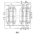
- FIG. 2 is a partially enlarged view to show the details of the two cell arrays located on the right and left ends of the semiconductor memory device shown in Fig. 1, 14 cell arrays therebetween being omitted
- the same component elements are given the same reference numbers.
- the I/O lines comprise correspondingly the first I/O lines 10a connected to the first bit line group and the second I/O lines 10b connected to the second bit line group.
- the first and the second I/O lines 10a and 10b each comprise two pairs of I/O line consisting of two signal lines that are complementary to each other, and extend in opposite directions from the substantial center toward the opposing longer sides of the semiconductor chip 1 in parallel to the word line of the cell array 4. These I/O lines are connected to I/O line selection circuits 6a and 6b respectively.
- the I/O line selection circuits 6a, 6b connect either one of the two 1/O line pairs on one end to one of the I/O line pairs at the other end depending on the control signal.
- the I/O pair at the other end is connected to the buffer circuit 5a or 5b.
- the buffer circuit 5a or 5b amplifies the potential of one of the I/O line pairs and controls supply of this amplified potential to either of the common data buses 2a or 2b (in case of read-out operation). Alternately, the buffer circuit amplifies the data supplied from the common data buses 2a, 2b and transmits the same to the I/O line pairs as a set of complementary data.
- the common data buses 2a, 2b each comprise two signal lines, are disposed along the two opposing longer sides of the semiconductor chip 1, and are connected with plural predetermined buffer circuits 5.
- the input/output pads DQ0, DQ1, DQ2 and DQ3 are provided on the two opposing longer sides of the chip in the number of two.
- the input/output pad DQ0 is connected to one of the signal lines of the common data bus 2b via the input/output buffer 7-0.
- the input/output pad DQ1 is connected to the other signal line of the common data bus 2b via the input/output buffer 7-1.
- the input/output pad DQ2 is connected to one of the signal lines of the common data bus 2a via the input/output buffer 7-2, and the input/output pad DQ3 to the other signal line of the common data bus 2a via the input/output buffer 7-3.
- a control signal generator 21 is provided on one of the shorter sides of the semiconductor chip 1 and supplies control signals such as the one for controlling the selection operations of the I/O line selection circuits 6a, 6b provided respectively on the two opposing longer sides of the chip 1, and the one for activating the buffer circuits 5a, and 5b.
- the data line extending from the memory cell array 4 to the input/output pads DQ2, DQ3 provided along one of the longer sides of the semiconductor chip 1 is a channel extending from the first I/O line 10a connected to the first bit line group to the input/output pads DQ2, DQ3 via the common data bus 2a and the buffers 7-2, 7-3
- the data line extending to the input/output pads DQ0, DQ1 on the other longer side is a channel extending from the second I/O line 10b connected to the second bit line group to the input/output pads DQ0, DQ1 via the colon data bus 2b and the buffers 7-0, 7-1.
- the entire data line length for one of the input/output pad groups (e.g. DQ2 and DQ3), unlike the prior art, will not be longer than the data line for the other group (e.g. DQ0 and DQ1).
- the length of the I/O lines 10a, 10b corresponds to one half of the length of the side of the memory cell array 4 in the word line direction and becomes therefore half the length in the prior art, the length of the data line itself can also be reduced.
- one memory cell array required a region wide enough to accommodate 4 pairs of I/O lines, or 8 signal lines.
- the first I/O line 10a and the second I/O line 10b each comprising four signal lines are provided to extend in the opposite directions, the width of the region for accommodating the I/O lines can be reduced to one half, contributing to integration of the semiconductor memory device.
- the number of lines for supplying control signals to these circuits become layer than in the prior art.
- the performance of a semiconductor memory device is determined mainly by the time involved in the data read-out, and the increase in the operational speed achieved by the reduced data line length outweighs the increased number of lines for the control signals.
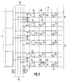
- FIG. 3 is a circuit diagram to show the specific construction of the circuit for the memory cell array 4, a selection switch SE, and I/O lines 10a and 10b.
- the same component elements as in Figs. 1 and 2 are given the same reference numbers.
- the memory cell array 4 is an array of so-called one-transistor one-capacitor type cell MSs, each of which comprising one N-channel MOS transistor and one capacitor element. Total of 1024 bit lines is divided into a first bit line group B1 and a second bit line group B2 with 512 lines each, so that the memory cell array 4 is divided into two regions 4a and 4b.
- bit lines BL each comprising a pair of lines are connected to respective sense amplifiers SA.
- the row decoder 2 (Figs. 1, 2) selects one of the word lines WL.
- the column decoder 3 supplies selection signals to the selection circuit SE to select two sense amplifiers SA in each of the bit line groups B1 and B2.
- the selection switch SE comprises a group of transistors which receive selection signals from the column decoder via gates and whose drain-source channel is provided between the input/output terminal of the sense amplifier SA and the I/O lines 10a, 10b.
- Two of the four bit line pairs selected by the column decoder 3 and the selection switch SE are connected to two pairs of signal lines 101a, 1O1b and signal lines 102a, 102b constituting the first I/O line 10a, while the remaining two pairs are connected to the second I/O line 10b.
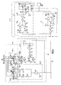
- FIG. 4 a specific construction of the circuit including the I/O line selection circuit 6a, buffer circuit 5a, input/output buffer 7-3 on the side of the first I/O line 10a will be described.
- the same component elements as in Figs. 1 and 2 are given the same reference numbers.
- the I/O line selection circuit 6a includes an I/O line selection circuit 6a-1 which operates during reading-out and an I/O line selection circuit 6a-2 which operates during writing-in.
- the I/O line selection circuit 6a-1 for reading includes transistors Q1 and Q2 which receive on gates control signal SLa from the control signal generator 21 (Fig.
- the I/O line selection circuit 6a-2 for writing includes transistors Q65 and Q66 which receive control signal SLc from the control signal generator 21 (Fig. 2) at their gates and of which source/drain paths are provided between signal lines 101a and 104a and between signal lines 101b and 104b, and transistors Q67 and Q68 which receive control signal SLd from the generator at their gates and of which source/drain paths are provides between signal lines 102a and 104a and between signal/lines 102b and 104b so as to select either one of the two pairs of signal lines 101a, 101b and 102a, 102b of the first I/O line 101 and to connect the selected one to the pair of signal lines 104a and 104b.
- the buffer circuit 5a includes a buffer circuit 5a-1 which operates for reading-out and a buffer circuit 5a-2 which operates for writing-in.
- the buffer circuit 5a-1 includes two differential circuits 51 and 52 of the same structure and three inverters 53, 54 and 55.
- the first differential circuit 51 includes transistors Q7 and Q8 which connects a pair of signal lines 103a, 103b to gates respectively and generates differential pair, is loaded by a current mirror circuit comprising transistors Q5 and Q6, and is activated with an activation signal AC supplied from the generator 21.
- the second differential circuit 52 is connected for one more stage with the first differential circuit 51, and the second differential circuit 52 is connected on one of the input/outputs thereof to an input of a transfer gate TG via the three inverter circuits for output 53, 54 and 55.
- the transfer gate TG1 determines by control whether or not to connect the input/output to the common data bus 2a in accordance with the control signal SLc.
- the buffer circuit 51-2 for writing-in includes a NAND gate 56 and three inverters 57, 58 and 59.
- the NAND gate 56 simplifies and inverts the writing-in data supplied to the common data bus 2a in accordance with the control signal SLf supplied from the generator 21.
- One of the outputs from the NAND gate 56 is outputted to the signal line 104b via the inverters 57, 58 while the other output therefrom is outputted to the signal line 105a via the inverter 59. This makes the levels of the signal lines 104a and 104b complementary to one another.
- the common data bus 2a is connected to the input/output pad DQ3 via an output buffer 71 and an input buffer 72 within the buffer circuit 7-3.
- the output data signal is further amplified by the inverters 71 and 72, and turned into two complementary signals by the NAND gate 74 which receives as inputs the amplified signal and a control signal ⁇ 1 supplied from the control signal generator 21 and by the NAND gate 75 which receives as inputs the amplified signal and the inversion of the control signal ⁇ 1.
- the write-in data supplied at the input/output pad DQ3 is further amplified by the inverters 76 and 77.
- the transfer gate TG2 controls whether or not the amplified signal should be connected to a latch circuit comprising inverters 79 and 80 in accordance with the control signal ⁇ 2. As the transfer gate TG2 is turned off by the control signal ⁇ 2, the transfer gate TG3 also controlled by the signal ⁇ 2 becomes active and the write-in data is latched by the latch circuit.
- the latched data is further amplified by an NAND gate 81 and an inverter 82 whose outputs are controlled by a control signal ⁇ 3.
- the NAND gate 84 which receives as input the amplified signal and a control signal ⁇ 4 and the NAND gate 85 which receives as inputs the amplified signal and an inversion of the control signal ⁇ 4 generate two complementary signals therefrom.
- the complementary signals are applied at the gate of a P channel transistor Q12 whose source-drain channel constituting CMOs is connected between the power source and an output and at the gate of an N channel transistor Q13 whose source-drain channel is connected between an output and the grounded potential, and the output signals therefrom are supplied to the common data bus 2a.
- the output of the output buffer 72 is held at high impedance by the control signal ⁇ 4 and separated from the common data bus 2a except for during the reading-out of data.
- buffer circuits 7-0, 7-1 and 7-2 are of the same construction as the buffer circuit 7-3, and are respectively connected to the input/output pads DQ0, DQ1, DQ2 and DQ3 whose respective input/outputs are disposed on the side of the opposing longer sides of the semi-conductor chip in the unit of two.
- the second embodiment differs from the first embodiment shown in Fig. 2 in that the common data buses are divided into four sets 30, 31, 32 and 33, each set comprising two complementary signal line pairs, or four signal lines, that the output signals from the buffer circuits 35a and 35b that supply signals to respective common data buses are complementary to each other, or two outputs, and that each of the common data buses 30, 31, 32 and 33 is provided with a common data bus selection circuit 9.
- the common data bus selection circuit 9 selects one of the two common data bus pairs that are connected thereto, amplifies one of the signals of the selected data bus and transmits the same to the buffer circuit 7. Alternately, the circuit 9 amplifies the write-in data from the buffer circuit 7 to generate complementary data, and transmits the same to the selected common data bus pair.
- Other features of the construction are identical with the embodiment shown in Figs. 1 through 4.
- the buffer circuits 33a and 35b may be constructed as the known two-way buffers.
- the common data bus selection circuit 9 may be constructed similarly to the I/O line selection circuit 6a-1 and the buffer circuit 5a-1 shown in Fig. 4, so as to enable it to select one of the two signal line pairs and to amplify the same.
- memory cell arrays belonging to respective input/output pads DQ0, DQ1, DQ2 and DQ3 can be distinctly blocked so that noises from the adjacent arrays during read-out can be easily dealt with.
- the present invention has been described with respect to DRAM, but it is applicable to SRAM (static RAM) I/O circuit, and PROM (programmable read-only memory), EPROM (erasable PROM) and EEPROM (electrically erasable PROM) read out circuits.
- SRAM static RAM
- PROM programmable read-only memory
- EPROM erasable PROM
- EEPROM electrically erasable PROM
Landscapes
- Dram (AREA)
Applications Claiming Priority (2)
| Application Number | Priority Date | Filing Date | Title |
|---|---|---|---|
| JP79216/90 | 1990-03-28 | ||
| JP7921690 | 1990-03-28 |
Publications (3)
| Publication Number | Publication Date |
|---|---|
| EP0454998A2 true EP0454998A2 (de) | 1991-11-06 |
| EP0454998A3 EP0454998A3 (en) | 1993-03-17 |
| EP0454998B1 EP0454998B1 (de) | 1995-11-08 |
Family
ID=13683736
Family Applications (1)
| Application Number | Title | Priority Date | Filing Date |
|---|---|---|---|
| EP91104961A Expired - Lifetime EP0454998B1 (de) | 1990-03-28 | 1991-03-27 | Halbleiterspeichereinrichtung |
Country Status (4)
| Country | Link |
|---|---|
| US (1) | US5097313A (de) |
| EP (1) | EP0454998B1 (de) |
| KR (1) | KR940004518B1 (de) |
| DE (1) | DE69114345T2 (de) |
Cited By (4)
| Publication number | Priority date | Publication date | Assignee | Title |
|---|---|---|---|---|
| EP0645696A1 (de) * | 1993-09-29 | 1995-03-29 | Kabushiki Kaisha Toshiba | Halbleiter-Speichergerät, das einen seriellen Zeiger benutzt |
| EP0683493A3 (de) * | 1994-05-20 | 1995-12-27 | Samsung Electronics Co Ltd | |
| EP0704847A1 (de) * | 1994-09-22 | 1996-04-03 | Kabushiki Kaisha Toshiba | Dynamischer Speicher mit geteillten Leseverstärkern |
| EP0814478A2 (de) * | 1996-06-19 | 1997-12-29 | Cirrus Logic, Inc. | Multi-Bank-Multi-Tor-Speicher und Systeme und diese verwendendes Verfahren |
Families Citing this family (5)
| Publication number | Priority date | Publication date | Assignee | Title |
|---|---|---|---|---|
| US5835395A (en) * | 1991-02-07 | 1998-11-10 | Texas Instruments Incorporated | Eprom pinout option |
| US5802005A (en) * | 1996-09-23 | 1998-09-01 | Texas Instruments Incorporated | Four bit pre-fetch sDRAM column select architecture |
| KR100280287B1 (ko) | 1998-08-28 | 2001-03-02 | 윤종용 | 반도체 메모리 장치 |
| KR100481174B1 (ko) * | 2002-08-02 | 2005-04-07 | 삼성전자주식회사 | 메모리 코어의 전 영역에서 동일한 스큐를 가지는 반도체메모리 장치 |
| US6975527B1 (en) * | 2002-11-12 | 2005-12-13 | Integrated Device Technology, Inc. | Memory device layout |
Citations (3)
| Publication number | Priority date | Publication date | Assignee | Title |
|---|---|---|---|---|
| EP0166642A2 (de) * | 1984-05-30 | 1986-01-02 | Fujitsu Limited | Blockunterteiltes Halbleiterspeichergerät mit unterteilten Bitzeilen |
| US4658377A (en) * | 1984-07-26 | 1987-04-14 | Texas Instruments Incorporated | Dynamic memory array with segmented bit lines |
| DE3916784A1 (de) * | 1988-07-29 | 1990-02-01 | Mitsubishi Electric Corp | Dynamische halbleiterspeichereinrichtung |
Family Cites Families (4)
| Publication number | Priority date | Publication date | Assignee | Title |
|---|---|---|---|---|
| EP0344873B1 (de) * | 1982-06-30 | 1993-12-15 | Fujitsu Limited | Integrierte Halbleiterschaltungsanordnung |
| US4962322A (en) * | 1988-12-05 | 1990-10-09 | Texas Instruments Incorporated | Nonvolatible capacitor random access memory |
| JPS6367771A (ja) * | 1986-09-09 | 1988-03-26 | Mitsubishi Electric Corp | 半導体記憶装置 |
| US4945393A (en) * | 1988-06-21 | 1990-07-31 | At&T Bell Laboratories | Floating gate memory circuit and apparatus |
-
1991
- 1991-03-27 DE DE69114345T patent/DE69114345T2/de not_active Expired - Lifetime
- 1991-03-27 EP EP91104961A patent/EP0454998B1/de not_active Expired - Lifetime
- 1991-03-28 US US07/676,509 patent/US5097313A/en not_active Expired - Lifetime
- 1991-03-28 KR KR1019910004901A patent/KR940004518B1/ko not_active IP Right Cessation
Patent Citations (3)
| Publication number | Priority date | Publication date | Assignee | Title |
|---|---|---|---|---|
| EP0166642A2 (de) * | 1984-05-30 | 1986-01-02 | Fujitsu Limited | Blockunterteiltes Halbleiterspeichergerät mit unterteilten Bitzeilen |
| US4658377A (en) * | 1984-07-26 | 1987-04-14 | Texas Instruments Incorporated | Dynamic memory array with segmented bit lines |
| DE3916784A1 (de) * | 1988-07-29 | 1990-02-01 | Mitsubishi Electric Corp | Dynamische halbleiterspeichereinrichtung |
Cited By (11)
| Publication number | Priority date | Publication date | Assignee | Title |
|---|---|---|---|---|
| EP0645696A1 (de) * | 1993-09-29 | 1995-03-29 | Kabushiki Kaisha Toshiba | Halbleiter-Speichergerät, das einen seriellen Zeiger benutzt |
| US5469400A (en) * | 1993-09-29 | 1995-11-21 | Kabushiki Kaisha Toshiba | Semiconductor memory device using serial pointer |
| US5561633A (en) * | 1993-09-29 | 1996-10-01 | Kabushiki Kaisha Toshiba | Semiconductor memory device using serial pointer |
| EP0683493A3 (de) * | 1994-05-20 | 1995-12-27 | Samsung Electronics Co Ltd | |
| EP0704847A1 (de) * | 1994-09-22 | 1996-04-03 | Kabushiki Kaisha Toshiba | Dynamischer Speicher mit geteillten Leseverstärkern |
| US5586078A (en) * | 1994-09-22 | 1996-12-17 | Kabushiki Kaisha Toshiba | Dynamic type memory |
| EP1081711A2 (de) | 1994-09-22 | 2001-03-07 | Kabushiki Kaisha Toshiba | Dynamischer Speicher |
| CN1134016C (zh) * | 1994-09-22 | 2004-01-07 | 株式会社东芝 | 动态存储器 |
| EP1081711A3 (de) * | 1994-09-22 | 2008-04-09 | Kabushiki Kaisha Toshiba | Dynamischer Speicher |
| EP0814478A2 (de) * | 1996-06-19 | 1997-12-29 | Cirrus Logic, Inc. | Multi-Bank-Multi-Tor-Speicher und Systeme und diese verwendendes Verfahren |
| EP0814478A3 (de) * | 1996-06-19 | 1998-10-28 | Cirrus Logic, Inc. | Multi-Bank-Multi-Tor-Speicher und Systeme und diese verwendendes Verfahren |
Also Published As
| Publication number | Publication date |
|---|---|
| EP0454998A3 (en) | 1993-03-17 |
| US5097313A (en) | 1992-03-17 |
| DE69114345T2 (de) | 1996-05-23 |
| DE69114345D1 (de) | 1995-12-14 |
| EP0454998B1 (de) | 1995-11-08 |
| KR940004518B1 (ko) | 1994-05-25 |
Similar Documents
| Publication | Publication Date | Title |
|---|---|---|
| JP3803050B2 (ja) | 半導体記憶装置、ダイナミックランダムアクセスメモリおよび半導体装置 | |
| KR100820294B1 (ko) | 반도체기억장치 | |
| US5357478A (en) | Semiconductor integrated circuit device including a plurality of cell array blocks | |
| US7638871B2 (en) | Semiconductor device | |
| US7254068B2 (en) | Semiconductor memory device | |
| US6191999B1 (en) | Semiconductor memory device with reduced power consumption | |
| US6504770B2 (en) | Semiconductor memory | |
| WO2000051184A1 (fr) | Dispositif a circuit integre en semiconducteur | |
| EP0454998B1 (de) | Halbleiterspeichereinrichtung | |
| US6867993B2 (en) | Semiconductor memory device | |
| US5694352A (en) | Semiconductor memory device having layout area of periphery of output pad reduced | |
| EP0788109B1 (de) | Integrierte Halbleiterschaltung mit verbesserter Eingangspfadverkabelung | |
| JP2725467B2 (ja) | 半導体メモリ装置 | |
| US6104627A (en) | Semiconductor memory device | |
| US6304478B1 (en) | Layout for a semiconductor memory | |
| US6069835A (en) | Semiconductor memory device | |
| JP2000058772A (ja) | 半導体メモリ装置 | |
| US6396756B1 (en) | Integrated circuit memory devices including transmission parts that are adjacent input/output selection parts | |
| JP2006140466A (ja) | 半導体記憶装置 | |
| KR20000026168A (ko) | 리드 멀티플렉서 | |
| US5949699A (en) | Semiconductor integrated circuit device | |
| KR100567019B1 (ko) | 싱크로너스 dram장치의 구조 | |
| KR19990086386A (ko) | 계층적 비트라인 구조를 갖는 반도체 메모리장치 | |
| JPH02170442A (ja) | 半導体集積回路装置 |
Legal Events
| Date | Code | Title | Description |
|---|---|---|---|
| PUAI | Public reference made under article 153(3) epc to a published international application that has entered the european phase |
Free format text: ORIGINAL CODE: 0009012 |
|
| 17P | Request for examination filed |
Effective date: 19910327 |
|
| AK | Designated contracting states |
Kind code of ref document: A2 Designated state(s): DE FR GB |
|
| PUAL | Search report despatched |
Free format text: ORIGINAL CODE: 0009013 |
|
| AK | Designated contracting states |
Kind code of ref document: A3 Designated state(s): DE FR GB |
|
| RHK1 | Main classification (correction) |
Ipc: G11C 7/00 |
|
| 17Q | First examination report despatched |
Effective date: 19950103 |
|
| GRAA | (expected) grant |
Free format text: ORIGINAL CODE: 0009210 |
|
| AK | Designated contracting states |
Kind code of ref document: B1 Designated state(s): DE FR GB |
|
| REF | Corresponds to: |
Ref document number: 69114345 Country of ref document: DE Date of ref document: 19951214 |
|
| ET | Fr: translation filed | ||
| PLBE | No opposition filed within time limit |
Free format text: ORIGINAL CODE: 0009261 |
|
| STAA | Information on the status of an ep patent application or granted ep patent |
Free format text: STATUS: NO OPPOSITION FILED WITHIN TIME LIMIT |
|
| 26N | No opposition filed | ||
| REG | Reference to a national code |
Ref country code: GB Ref legal event code: IF02 |
|
| REG | Reference to a national code |
Ref country code: GB Ref legal event code: 732E |
|
| REG | Reference to a national code |
Ref country code: FR Ref legal event code: TQ |
|
| REG | Reference to a national code |
Ref country code: GB Ref legal event code: 732E |
|
| REG | Reference to a national code |
Ref country code: FR Ref legal event code: TP |
|
| PGFP | Annual fee paid to national office [announced via postgrant information from national office to epo] |
Ref country code: FR Payment date: 20100324 Year of fee payment: 20 |
|
| PGFP | Annual fee paid to national office [announced via postgrant information from national office to epo] |
Ref country code: GB Payment date: 20100322 Year of fee payment: 20 |
|
| PGFP | Annual fee paid to national office [announced via postgrant information from national office to epo] |
Ref country code: DE Payment date: 20100429 Year of fee payment: 20 |
|
| REG | Reference to a national code |
Ref country code: FR Ref legal event code: CD |
|
| REG | Reference to a national code |
Ref country code: DE Ref legal event code: R071 Ref document number: 69114345 Country of ref document: DE |
|
| REG | Reference to a national code |
Ref country code: GB Ref legal event code: PE20 Expiry date: 20110326 |
|
| PG25 | Lapsed in a contracting state [announced via postgrant information from national office to epo] |
Ref country code: GB Free format text: LAPSE BECAUSE OF EXPIRATION OF PROTECTION Effective date: 20110326 |
|
| PG25 | Lapsed in a contracting state [announced via postgrant information from national office to epo] |
Ref country code: DE Free format text: LAPSE BECAUSE OF EXPIRATION OF PROTECTION Effective date: 20110327 |