EP0453759B1 - CMOS-rückkopplungsempfindlicher Verstärker mit Hochgeschwindigkeitsrückkopplung - Google Patents
CMOS-rückkopplungsempfindlicher Verstärker mit Hochgeschwindigkeitsrückkopplung Download PDFInfo
- Publication number
- EP0453759B1 EP0453759B1 EP91104216A EP91104216A EP0453759B1 EP 0453759 B1 EP0453759 B1 EP 0453759B1 EP 91104216 A EP91104216 A EP 91104216A EP 91104216 A EP91104216 A EP 91104216A EP 0453759 B1 EP0453759 B1 EP 0453759B1
- Authority
- EP
- European Patent Office
- Prior art keywords
- transistor
- electrode connected
- gate electrode
- transistors
- node
- Prior art date
- Legal status (The legal status is an assumption and is not a legal conclusion. Google has not performed a legal analysis and makes no representation as to the accuracy of the status listed.)
- Expired - Lifetime
Links
Images
Classifications
-
- G—PHYSICS
- G11—INFORMATION STORAGE
- G11C—STATIC STORES
- G11C11/00—Digital stores characterised by the use of particular electric or magnetic storage elements; Storage elements therefor
- G11C11/21—Digital stores characterised by the use of particular electric or magnetic storage elements; Storage elements therefor using electric elements
- G11C11/34—Digital stores characterised by the use of particular electric or magnetic storage elements; Storage elements therefor using electric elements using semiconductor devices
- G11C11/40—Digital stores characterised by the use of particular electric or magnetic storage elements; Storage elements therefor using electric elements using semiconductor devices using transistors
- G11C11/401—Digital stores characterised by the use of particular electric or magnetic storage elements; Storage elements therefor using electric elements using semiconductor devices using transistors forming cells needing refreshing or charge regeneration, i.e. dynamic cells
- G11C11/4063—Auxiliary circuits, e.g. for addressing, decoding, driving, writing, sensing or timing
- G11C11/407—Auxiliary circuits, e.g. for addressing, decoding, driving, writing, sensing or timing for memory cells of the field-effect type
-
- G—PHYSICS
- G11—INFORMATION STORAGE
- G11C—STATIC STORES
- G11C7/00—Arrangements for writing information into, or reading information out from, a digital store
- G11C7/06—Sense amplifiers; Associated circuits, e.g. timing or triggering circuits
- G11C7/065—Differential amplifiers of latching type
Definitions
- This invention relates to sense amplifier circuits useful in CMOS integrated circuits and, more particularly, to regenerative amplifier circuits for quickly and correctly sensing small differential voltage signals.
- MOS regenerative sense amplifiers latch differential signals at high speed.
- a fast NMOS latching operation may pull the sense amplifier input node with the high voltage signal down significantly, possibly as far down as V CC /2. This creates the possibility that the wrong side of the amplifier may conduct causing an erroneous output.
- the vagaries of semiconductor processing cause an imbalance in the physical parameters of the sense amplifier, the likelihood of improper conduction and latching increases.
- imbalances in the transconductances, g m , or threshold voltages, V T , of the cross-coupled transistors which typically form a latch in the sense amplifier, or in the capacitive loads of the inputs of the sense amplifier could cause improper conduction and latching.
- High speed sense amplifiers are typically used for reading s tatic r andom a ccess m emory (SRAM) cells and imbalances in such memory cells themselves are possibilities.
- the document US-A-4,843,264 disclosese a dynamic sense amplifier for use in static random access memory having a pair of differential bit lines.
- the sense amplifier comprises two sensing transistors having gate electrodes coupled to a pair of differential input nodes, and the two sensing transistors are coupled with their source electrodes to a common pull-down node.
- a pull-down transistor is provided for drawing current from the pull-down node during sense operation.
- a latch comprising four transistors is coupled to the drains of the sensing transistors for generating a pair of amplified differential signals on two latch output nodes wherein the four-transistor latch comprises two cross-coupled CMOS inverters.
- Transfer means are provided for generating two signals on two isolation nodes which correspond to the voltage levels on said latch output nodes, the transfer means including two CMOS inverters and each of said CMOS inverters has gate electrodes coupled to one of said latch output nodes and a source node coupled to said pull-down node.
- Output drivers are coupled to the isolation nodes for generating an output signal on a driver output node wherein the output signal corresponds to the voltage levels on the latch output nodes.
- Precharge means are provided for precharging the latch output nodes and the isolation node between sensing operations. When the pull-down transistor is activated, the four-transistor latch automatically amplifies the voltage differential on the gates of the sensing transistors thereby generating a pair of differential output signals.
- the latch is closely coupled to the output drivers providing fast propagation of data read from a memory cell to the driver output node.
- the present invention as defined in the independent claims 1 and 10 solves or substantially mitigates such problems in high speed latching operations.
- the present invention provides for a sense amplifier having a pair of input nodes connected through isolating MOS transistors to the differential input terminals of the amplifier.
- Each of the input nodes is also connected to the gate electrode of one of a pair of carefully matched NMOS transistors and to the drain electrodes of the other of the matched pair.
- each of the input nodes is connected to the gate electrode of one of two drive NMOS transistors.
- the drain electrodes of the drive transistors are connected respectively to the gate electrodes of two output transistors, the drain electrodes of which form the output terminals of the sense amplifier.
- the source electrodes of the matched NMOS transistor pair are coupled to ground by a NMOS transistor.
- the source electrodes of the drive NMOS transistors are also coupled to ground by a second NMOS transistor.
- the source electrodes of the matched NMOS transistor pair and the source electrodes of the drive NMOS transistors are pulled to ground in a timed relationship.
- the input nodes of the amplifier are pulled toward ground in a high-speed operation, the input node at the higher voltage is still able to turn on its corresponding drive NMOS transistor. Latching of the sense amplifier proceeds safely.
- the sense amplifier has a pair of cross-coupled PMOS transistors, each having a source electrode connected to the high supply voltage, a drain electrode connected to the drain electrode of one of the drive transistors, and a gate electrode connected to the drain electrode of the other cross-coupled PMOS transistor.
- the cross-coupled PMOS transistors ensure that only one of the output transistors turns on.
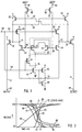
- Fig. 1 is a circuit diagram of a preferred embodiment of the present invention.
- Fig. 2 is a timing diagram of the operation of the circuit shown in Fig. 1.
- the circuit of Fig. 1 has true and complementary input terminals 61, 62 which receive differential voltage signals for sensing.
- the terminal 61 and the terminal 62 are coupled to the bit line and the complementary bit line, respectively, of an array of static RAM (SRAM) cells.
- SRAM static RAM
- the selected cell is accessed and a differential voltage starts developing on the bit line and its complement.
- the differential is small, of the order of 0.1 volts, compared to the voltage on the bit lines, which are typically held near the positive supply voltage, V CC (+5 volts) in the present case.
- the negative supply voltage is ground.
- the input terminals 61 and 62 are respectively connected to the source electrodes of PMOS transistors 11 and 12. (In passing, it should be noted that the drawings use the symbol of an MOS transistor with a bubble over the gate to indicate a PMOS transistor.)
- the drain electrodes of the PMOS transistors 11 and 12 are connected to the input nodes 65 and 66 of a regenerative sense amplifier stage 20, respectively.
- the PMOS transistors 11 and 12 serve the function of isolating the capacitances of the bit lines from the latching input nodes 65 and 66 during a sensing operation.
- the gate electrodes of both transistors 11 and 12 are held low so that the transistors are turned on. While passing voltage signals from the bit lines to the input nodes 65 and 66, the PMOS transistors 11 and 12 present high impedances between the bit lines and the input nodes.
- Fig. 1 shows the PMOS transistors 11 and 12 to be permanently on, the gate electrodes of these transistors could be connected to an address decoder as part of column selection in an SRAM array.
- the input nodes 65 and 66 of the amplifier stage 20 are connected to two cross-coupled and carefully matched NMOS transistors 21 and 22.
- the drain electrode of the transistor 21 is connected to the gate electrode of the transistor 22 (and the input node 66) and the drain electrode of the transistor 22 is connected to the gate electrode of the transistor 21 (and the input node 65).
- the source electrodes of both transistors 21, 22 form a supply voltage node which is connected to a node 76 which is formed by the common drain electrodes of a complementary pair of transistors 41 and 42.
- the source electrode of the PMOS transistor 41 is connected to the voltage reference at V CC , which is typically +5 volts, while the source electrode of the NMOS transistor 42 is connected to a voltage reference at ground.
- the gate electrodes of both transistors 41, 42 are connected to a control signal terminal 69 by a line 54.
- the NMOS transistor 42 is large compared to the capacitance at the node 76 so as to able to pull the node 76 down toward ground quickly when the signal at the control terminal 69 goes high.
- the input nodes 65 and 66 are respectively connected to the gate electrodes of the NMOS drive transistors 23 and 24 respectively.
- the source electrodes of both transistors 23 and 24 are connected to a node 75 formed by the common drain electrodes of a complementary pair of transistors 43 and 44.
- the source electrode of the PMOS transistor 43 is connected to the voltage reference at V CC and the source electrode of the NMOS transistor 44 is connected to the voltage reference at ground.
- the gate electrodes of both transistors 43 and 44 are connected to the control signal terminal 69 by a line 54.
- the NMOS transistor 44 is sized smaller relative to the capacitance at the node 75 compared to the size of the transistor 42 relative to the capacitance at the node 76.
- the drain electrodes of the drive transistors 23 and 24 are respectively connected to the drain electrodes of PMOS precharge transistors 25 and 26 and the connections respectively form the nodes 71 and 72.
- the source electrodes of both PMOS transistor 25 and 26 are connected to the V CC voltage reference and the gate electrodes of both transistors 25 and 26 are connected by a line 53 to the control signal terminal 69.
- the nodes 71 and 72 are respectively connected to the gate electrodes of PMOS output transistors 31 and 32.
- the source electrodes of both transistors 31 and 32 are connected to the V CC supply voltage and the drain electrodes are connected respectively to the output terminals 63 and 64 of the sense amplifier of the present invention.
- the output lines connected to the output terminals 63 and 64 are held near ground by NMOS transistors when the sense amplifier is not in operation.
- the NMOS transistors release the output lines so that one of the output terminals 63 or 64 can go high for a differential output signal.
- the nodes 71 and 72 are also respectively connected to the drain electrodes of PMOS transistors 33 and 34, which are cross-coupled.
- a line 51 connects the gate electrode of the transistor 33 to the drain electrode of the transistor 34 and a line 52 connects the gate electrode of the transistor 34 to the drain electrode of the transistor 33.
- the PMOS transistors 33 and 34 are not required if the circuit of the present invention is implemented ideally. In theory, the two transistors 33 and 34 may be deleted without an adverse effect of the sense amplifier of the present invention.
- the control signal on the terminal 69 is low, 0 volts or ground. Both PMOS transistors 25 and 26 are on to "precharge" the nodes 71 and 72 to V CC . Both the nodes 71 and 72 are high and the PMOS output transistors 31 and 32 are off. Provision (not shown) is made to discharge the output terminals 63 and 64 to ground at this time. Both input nodes 65 and 66 are pulled high by the high voltage of the bit line and its complement acting through the PMOS transistors 11 and 12 respectively.
- the sense amplifier is engaged after one of the SRAM cells of the array is selected for a sensing operation.
- the state of the selected cell appears as a small differential voltage between the bit line and its complement, both nominally near the +5 volt potential of VCC.
- the bit line voltage passes through the input terminal 61 and the PMOS transistor 11 to the input 65.
- the complementary bit line voltage passes through the input terminal 62 and the PMOS transistor 12 to the input node 66.
- the differential voltage appears at the input nodes 65 and 66 for sensing.
- the signal at the control terminal 69 now goes high.
- the PMOS transistors 25 and 26 are turned off. This frees the nodes 71 and 72, which were kept high by the action of the transistors 25 and 26.
- the high transition at the control signal terminal 69 turns on the NMOS transistor 42 and turns off the PMOS transistor 41 (if it exits) which rapidly pulls the node 76 toward ground.
- the cross-coupled NMOS transistors 21 and 22 turn on and begin their regenerative action. Since the input node 65 (and the gate electrode of the transistor 21) is at a higher voltage than the input node 66 (and the gate electrode of the transistor 22) and since the source electrodes are both at the same voltage, the transistor 21 draws more current from the input node 66 than does the transistor 22 from the input node 65. The node 66 falls faster than the node 65, increasing the voltage differential as desired.
- bit lines have very much larger capacitances than the input nodes of sense amplifiers.
- a bit line has a capacitance of approximately 1 pF, while an input node has a capacitance of approximately 0.1 pF.
- the PMOS transistors 11 and 12 separate the large capacitance of the bit lines from the input nodes by providing a large effective impedance between a bit line (or a complementary bit line) and a discharging input node.
- a bit line or a complementary bit line
- the voltage on the input nodes 65 or 66 can drop, while the voltages on the bit lines and their complements remain high.
- the node 76 As the node 76 is pulled to ground, two effects occur which effect the transistors 21 and 22.
- the first effect is wrongside conduction.
- the node 76 should be pulled to ground quickly as shown in Fig. 2. If such is done, then the voltage difference between the source and gate electrodes of both transistors 21 and 22 increase. Invariably for both transistors 21 and 22, the gate-to-source voltage exceeds V T , the threshold voltage of the transistors. Both transistors 21 and 22 are turned on. For the transistor receiving the more positive differential voltage at its gate, in the example of Fig. 2 the transistor 21, this is no problem. The transistor should be on. But for the transistor receiving the less positive voltage, transistor 22 in this case, this is not desirable.
- the second effect is the capacitive coupling between the gate electrode and the source/drain electrodes of both transistors 21 and 22.
- the source electrodes of both transistors also fall, capacitively pulling down the gate electrodes and both input nodes 65 and 66.
- the low node 66 this is no problem because it should move to ground.
- the high node 65 this is a problem because ideally it should remain at a high voltage. Again latching is slowed.
- the result of the two effects on the node 65 is shown in Fig. 2 as a dip in the voltage.
- the voltage on the node 65 remains high enough to pull the node 66 to near the ground reference potential.
- the present invention provides for the NMOS transistors 23 and 24 to ensure a high speed operation.
- the NMOS transistor 44 turns on while the PMOS transistor 43 (if present) turns off to pull the node 75 low. This action also pulls the source electrodes of the NMOS transistors 23 and 24 low.
- the node 75 is engineered to move slowly enough that the voltage difference between the gate electrode and the source electrode of the drive transistor (24, in this example), which is receiving the lower differential voltage at the input node 66, does not turn on.
- the drive transistor 23 turns on even though the input node 65 dips due to wrongside conduction and capacitive coupling, as explained previously.
- the node 71 is pulled low, as shown in Fig. 2, to turn on the PMOS output transistor 31.
- the voltage at the output terminal 63 rises.
- the drive transistor receiving the lower differential voltage in this case the drive transistor 24, should not turn on with the fall of the node 75. This is done by moderating the fall of the node 75 with respect to the fall of the node 76 so that voltage difference between the source electrode and the gate electrode of the drive transistor receiving the lower differential voltage, here the transistor 24, does not exceed the threshold voltage V T .
- the control of the rate of the node 75 fall with respect to the node 76 fall when the terminal 69 goes high is controlled by the proper sizing of the transistors 42 and 44 with respect to the nodes 76 and 75.
- the uncertainties in semiconductor processing such as in the operational characteristics of the transistors, the matching of the operational characteristics of the transistors and the capacitive loads at the various nodes of the circuit make reliance upon an ideal timing between the fall of the nodes 76 and 75 risky in an actual device.
- One alternative is to delay the fall of the node 75 until the sensing by transistors 21 and 22 is complete, but this would delay the final output.
- the PMOS transistors 33 and 34 Another alternative is provided by the PMOS transistors 33 and 34. These transistors ensure that even if the drive transistor receiving the lower differential voltage (transistor 24 in this example) turns on, the node 72 is held high to prevent the PMOS output transistor 32 from turning on. In the example of Fig. 2, the higher voltage at the input node 65 turns on the drive transistor 23 before the drive transistor 24 which ideally should remain off as the node 75 falls. This forces the node 71 to fall. By the line 52 the low voltage on the node 71 turns on the PMOS transistor 34 to hold the node 72 high. Thus even if the drive transistor 24 is somewhat turned on, the PMOS output transistor 32 stays off.
- the PMOS transistors 33 and 34 provide a safety margin for the vagaries of semiconductor processing.
- the PMOS transistors 41 and 43 which are used to restore the source electrodes of the transistors 21 and 22, and the transistors 23 and 24 respectively, to V CC after a sensing operation, are not strictly required. For example, after a sensing operation the control signal at the terminal 69 returns low and the NMOS transistors 42 and 44 are turned off. Even without the presence of the PMOS transistor 41, the node 76 rises from the conduction of the cross-coupled transistors 21 and 22. The node 76 is charged by the current through the transistor 21 from the input node 66 and by the current through the transistor 22 from the input node 65. Even though both nodes 65 and 66 carry a differential signal, both nodes are returning to near V CC . The node 76 rises to approximately V CC -V T , V T being the threshold voltage of the transistors 21 and 22, at which point both transistors 21 and 22 turn off.
- the PMOS transistor 43 is not strictly required for the recovery of the node 75 after sensing. Even without the PMOS transistor 43, one or both of the transistors 23 and 24 conducts current from the nodes 71 and 72 (which are high due to the precharging action of the PMOS transistors 25 and 26 respectively) to the node 75 until the node is charged up to V CC -V T , V T being the threshold voltage of the transistors 23 and 24.
- the advantage of the PMOS transistors 41 and 43 is the quick recovery of the sense amplifier after a sensing operation. As explained above, without the transistor 41 the cross-coupled transistors 21 and 22 remain on until the node 76 rises sufficiently to turn the transistors off. Assume the circuit is recovering form the sensing operation described earlier, in which the node 65 was at the higher voltage than was the node 66. Now with the node 65 higher than the node 66, more current to charge the node 76 comes through the transistor 21 than comes through the transistor 22. Current through the transistor 21 tries to pull the node 66 low at the very time we are trying to equilibrate the voltages on the nodes 65 and 66 (and on the input terminals 61 and 62). That is, this differential current slows down the equilibration process.
- the PMOS transistor 43 pulls the node 75 up quickly to turn off one or both of the drive transistors 23 and 24 for a fast equilibration of the nodes 71 and 72.
- the sense amplifier is ready for the next sensing operation.
- the PMOS transistor 41 also may be used to delay the fall of the node 76 when the control signal 69 starts to go high and that PMOS transistor 43 may be used to similarly delay the fall of the node 75.
- the present invention has proved effective in practice.
- the present sense amplifier has operated securely in high speed operations in which the regenerative sense amplifier stage has been pulled low in 200 picoseconds. Additionally even with the high voltage signal of the differential signal being pulled below V CC /2, the sense amplifier can operate securely. The only effect is to lengthen the time for the sense amplifier to latch, i.e., the access time is increased.
Landscapes
- Engineering & Computer Science (AREA)
- Microelectronics & Electronic Packaging (AREA)
- Computer Hardware Design (AREA)
- Static Random-Access Memory (AREA)
- Dram (AREA)
- Read Only Memory (AREA)
Claims (12)
- Ein MOS-Leseverstärker mit einem Paar von Differentialeingangsklemmen (61, 62) und einem Paar von Differentialausgangsklemmen (63, 64), umfassend:ein Paar von kreuzgekoppelten Transistoren (21, 22), wobei jeder Transistor mit einer Gate-Elektrode an eine Drain-Elektrode des anderen Transistors angeschlossen ist, mit einer Source-Elektrode an die Source-Elektrode des anderen kreuzgekoppelten Transistors angeschlossen ist zur Bildung eines ersten gemeinsamen Knotens (76);Mittel (11, 12) für das Verbinden einer Eingangsklemme mit der Gate-Elektrode eines der kreuzgekoppelten Transistoren und für das Verbinden der anderen Eingangsklemme mit der Gate-Elektrode des anderen kreuzgekoppelten Transistors;einen ersten Latch-Transistor (42) mit einer Drain-Elektrode angeschlossen an den ersten gemeinsamen Knoten, einer Source-Elektrode angeschlossen an eine erste Spannungsrefernz und einer Gate-Elektrode angeschlossen an einen ersten Steuersignalknoten (54);ein Paar von Treibertransistoren (23, 24), wobei jeder Transistor mit einer Gate-Elektrode jeweils mit der Gate-Elektrode eines der kreuzgekoppelten Transistoren verbunden ist, mit einer Source-Elektrode mit der Source-Elektrode des anderen Treibertransistors verbunden ist zur Bildung eines zweiten gemeinsamen Knotens (75) und mit einer Drain-Elektrode;einen zweiten Latch-Transistor (44) mit einer Drain-Elektrode mit dem zweiten gemeinsamen Knoten verbunden, einer Source-Elektrode mit der ersten Spannungsreferenz verbunden und mit einer Gate-Elektrode mit einem zweiten Steuersignalknoten (54) verbunden;ein Paar von Vorladetransistoren (25, 26), wobei jeder Transistor mit einer Drain-Elektrode jeweils eines des Treibertransistoren verbunden ist, mit einer Gate-Elektrode mit einem dritten Steuersignalknoten (53) verbunden ist und mit einer Source-Elektrode mit einer zweiten Spannungsreferenz verbunden ist; undein Paar von Ausgangstransistoren (31, 32), wobei jeder Transistor mit einer Source-Elektrode mit der zweiten Spannungsreferenz verbunden ist, mit einer Gate-Elektrode mit der Drain-Elektrode jeweils eines der Treibertransistoren verbunden ist und mit einer Drain-Elektrode mit jeweils einer der Ausgangsklemmen verbunden ist,wodurch der Leseverstärker ein Hochgeschwindigkeitsausgangssignal an den Ausgangsklemmen bei entsprechenden Lesebetriebssignalen an dem ersten, dem zweiten bzw. dritten Steuersignalknoten erzeugt, so daß das Potential des ersten gemeinsamen Knotens schneller auf die erste Referenzspannung abfällt als das Potential des zweiten gemeinsamen Knotens.
- Der Leseverstärker nach Anspruch 1, ferner umfassend ein zweites Paar von kreuzgekoppelten Transistoren (33, 34), wobei jeder Transistor mit einer Source-Elektrode mit der zweiten Spannungsreferenz verbunden ist, mit einer Drain-Elektrode mit der Drain-Elektrode eines der Treibertransistoren verbunden ist und mit einer Gate-Elektrode an die Drain-Elektrode des anderen kreuzgekoppelten Transistors angeschlossen ist.
- Der Leseverstärker nach Anspruch 1 oder 2, ferner umfassend einen Auffrischtransistor (41), der mit einer Source-Elektrode an der zweiten Spannungsreferenz liegt, mit einer Gate-Elektrode an dem ersten Steuersignalknoten (54) liegt und mit einer Drain-Elektrode an dem ersten gemeinsamen Knoten (76) liegt.
- Der Leseverstärker nach Anspruch 1 oder 2 oder 3, ferner umfassend einen Auffrischtransistor (43), der mit einer Source-Elektrode mit der zweiten Spannungsreferenz verbunden ist, mit einer Gate-Elektrode mit dem zweiten Steuersignalknoten (54) verbunden ist und mit einer Drain-Elektrode mit dem zweiten gemeinsamen Knoten (75) verbunden ist.
- Der Leseverstärker nach Anspruch 1, bei dem das Verbindungsmittel ein Paar von Widerstandsmitteln (11, 12) umfaßt, wobei jedes Widerstandsmittel eine Eingangsklemme mit jeweils der Gate-Elektrode eines der kreuzgekoppelten Transistoren (21, 22) verbindet und die andere Eingangsklemme mit der Gate-Elektrode des anderen kreuzgekoppelten Transistors verbindet.
- Der Leseverstärker nach Anspruch 5, bei dem das Paar von Widerstandsmitteln ein Paar von Transistoren (11, 12) umfaßt, wobei jeder Transistor eine Source-Elektrode mit einer der Eingangsklemmen verbunden aufweist und eine Drain-Elektrode mit der Gate-Elektrode des einen der kreuzgekoppelten Transistoren verbunden ist, wobei jeder Transistor einen Widerstand zwischen seiner entsprechenden Eingangsklemme und der Gate-Elektrode während eines Lesevorgangs bildet.
- Der Leseverstärker nach Anspruch 6, bei dem jeder Transistor (11, 12) des Paares eine Gate-Elektrode aufweist, welche Gate-Elektrode jedes Transistors mit der ersten Spannungsreferenz verbunden ist.
- Der Leseverstärker nach Anspruch 6, bei dem jeder des Transistorpaars (11, 12) eine Gate-Elektrode besitzt, welche Gate-Elektrode jedes Transistors mit einem Adreßdekoder verbunden ist.
- Der Leseverstärker nach Anspruch 1, 2, 3 oder 4, bei dem der erste, der zweite und der dritte Steuersignalknoten mit einer Steuersignalklemme (69) verbunden sind.
- Ein Verfahren zum Erzeugen eines Hochgeschwindigkeitsausgangssignals an den Ausgangsklemmen eines MOS-Leseverstärkers mit einem Paar von Differentialeingangsklemmen (61, 62), einem Paar von Differentialausgangsklemmen (63, 64); einem Paar von kreuzgekoppelten Transistoren (21, 22), wobei jeder Transistor mit einer Gate-Elektrode mit der Drain-Elektrode des anderen Transistors verbunden ist, einer Source-Elektrode mit der Source-Elektrode des anderen kreuzgekoppelten Transistors verbunden ist zur Bildung eines ersten gemeinsamen Knotens (76), Mitteln (11, 12) für das Verbinden einer Eingangsklemme mit der Gate-Elektrode eines der kreuzgekoppelten Transistoren für das Verbinden der anderen Eingangsklemme mit der Gate-Elektrode des anderen kreuzgekoppelten Transistors; einem ersten Latch-Transistor (42), der mit einer Drain-Elektrode mit dem ersten gemeinsamen Knoten verbunden ist, mit einer Source-Elektrode mit einer ersten Spannungsreferenz verbunden ist und einer Gate-Elektrode mit einem ersten Steuersignalknoten (54) verbunden ist; einem Paar von Treibertransistoren (23, 24), wobei jeder Transistor eine Gate-Elektrode aufweist verbunden mit der Gate-Elektrode jeweils eines der kreuzgekoppelten Transistoren, einer Source-Elektrode verbunden mit der Source-Elektrode des anderen Treibertransistors zur Bildung eines zweiten gemeinsamen Knotens (75) und einer Drain-Elektrode; einem zweiten Latch-Transistor (44) mit einer Drain-Elektrode verbunden mit dem zweiten gemeinsamen Knoten, einer Source-Elektrode verbunden mit der ersten Spannungsreferenz und einer Gate-Elektrode verbunden mit einem zweiten Steuersignalknoten (54); einem Paar von Vorladetransistoren (25, 26), wobei jeder Transistor eine Drain-Elektrode mit der Drain-Elektrode jeweils eines der Treibertransistoren verbunden aufweist, eine Gate-Elektrode verbunden mit einem dritten Steuersignalknoten (53) aufweist und eine Source-Elektrode verbunden mit einer zweiten Spannungsreferenz aufweist; und mit einem Paar von Ausgangstransistoren (31, 32), wobei jeder Transistor eine Source-Elektrode aufweist verbunden mit der zweiten Spannungsreferenz, eine Gate-Elektrode verbunden mit der Drain-Elektrode jeweils eines der Treibertransistoren und einer Drain-Elektrode verbunden mit jeweils einer der Ausgangsklemmen, welches Verfahren umfaßt:Erzeugen eines Steuersignals an dem dritten Steuersignalknoten zum Ausschalten der Vorladetransistoren (25, 26);Erzeugen eines Steuersignals an dem ersten Steuersignalknoten (54) zum Einschalten des ersten Latch-Transistors (42); undErzeugen eines Steuersignals an dem zweiten Steuersignalknoten (54) zum Einschalten des zweiten Latch-Transistors (44) derart, daß das Potential des zweiten gemeinsamen Knotens (75) langsamer abfällt als das Potential des ersten gemeinsamen Knotens auf das Potential der ersten Spannungsreferenz, so daß der Treibertransistor (24), der das tiefere Potential einer Spannungsdifferenz, angelegt an die Eingangsklemmen (61, 62) erhält, nicht eingeschaltet wird durch die Spannungsdifferenz zwischen seiner Source-Elektrode und seiner Gate-Elektrode.
- Das Verfahren nach Anspruch 10, umfassend den Schritt:Halten der Drain-Elektrode des Treibertransistors (24), dessen Gate-Elektrode die niedrigere Spannungsdifferenz empfängt nahe der zweiten Spannungsreferenz in Reaktion auf eine höhere Spannungsdifferenz an der Gate-Elektrode des anderen kreuzgekoppelten Transistors, um sicherzustellen, daß der Ausgangstransistor (32), verbunden mit dem Treibertransistor, dessen Gate-Elektrode die niedrigere Spannungsdifferenz erhält, nicht einschaltet.
- Das Verfahren nach Anspruch 10 oder 11, bei dem die Signale für den dritten Steuersignalknoten, den ersten Steuersignalknoten und den zweiten Steuersignalknoten im wesentlichen gleichzeitig erzeugt werden.
Applications Claiming Priority (2)
| Application Number | Priority Date | Filing Date | Title |
|---|---|---|---|
| US07/504,176 US5057718A (en) | 1990-04-03 | 1990-04-03 | Cmos regenerative sense amplifier with high speed latching |
| US504176 | 2000-02-15 |
Publications (2)
| Publication Number | Publication Date |
|---|---|
| EP0453759A1 EP0453759A1 (de) | 1991-10-30 |
| EP0453759B1 true EP0453759B1 (de) | 1996-05-08 |
Family
ID=24005176
Family Applications (1)
| Application Number | Title | Priority Date | Filing Date |
|---|---|---|---|
| EP91104216A Expired - Lifetime EP0453759B1 (de) | 1990-04-03 | 1991-03-19 | CMOS-rückkopplungsempfindlicher Verstärker mit Hochgeschwindigkeitsrückkopplung |
Country Status (5)
| Country | Link |
|---|---|
| US (1) | US5057718A (de) |
| EP (1) | EP0453759B1 (de) |
| JP (1) | JP2854439B2 (de) |
| KR (1) | KR100196487B1 (de) |
| DE (1) | DE69119294T2 (de) |
Families Citing this family (9)
| Publication number | Priority date | Publication date | Assignee | Title |
|---|---|---|---|---|
| US5272395A (en) * | 1991-04-05 | 1993-12-21 | Analog Devices, Inc. | CMOS strobed comparator |
| US5175450A (en) * | 1991-08-23 | 1992-12-29 | Micron Technology, Inc. | Apparatus for providing multi-level potentials at a sense node |
| US5132575A (en) * | 1991-08-23 | 1992-07-21 | Micron Technology, Inc. | Method for providing multi-level potentials at a sense node |
| US5345111A (en) * | 1992-08-19 | 1994-09-06 | Hyundai Electronics America | High-speed current sense amplifier |
| US5294847A (en) * | 1992-08-31 | 1994-03-15 | Motorola, Inc. | Latching sense amplifier |
| US5936432A (en) * | 1997-10-20 | 1999-08-10 | Hyundai Electronics America, Inc. | High speed low power amplifier circuit |
| KR100457345B1 (ko) * | 1997-11-25 | 2005-04-06 | 삼성전자주식회사 | 불 휘발성 반도체 메모리 장치 |
| US5982202A (en) * | 1998-05-13 | 1999-11-09 | Dallas Semiconductor Corporation | Method and apparatus for pre-biasing inputs to a latching portion of a sensing amplifier |
| US8975943B2 (en) | 2013-05-29 | 2015-03-10 | Silanna Semiconductor U.S.A., Inc. | Compact level shifter |
Family Cites Families (6)
| Publication number | Priority date | Publication date | Assignee | Title |
|---|---|---|---|---|
| JPS601712B2 (ja) * | 1980-12-04 | 1985-01-17 | 株式会社東芝 | 半導体記憶装置 |
| US4649301A (en) * | 1985-01-07 | 1987-03-10 | Thomson Components-Mostek Corp. | Multiple-input sense amplifier with two CMOS differential stages driving a high-gain stage |
| US4837465A (en) * | 1985-01-16 | 1989-06-06 | Digital Equipment Corp | Single rail CMOS register array and sense amplifier circuit therefor |
| US4716320A (en) * | 1986-06-20 | 1987-12-29 | Texas Instruments Incorporated | CMOS sense amplifier with isolated sensing nodes |
| US4791324A (en) * | 1987-04-10 | 1988-12-13 | Motorola, Inc. | CMOS differential-amplifier sense amplifier |
| US4843264A (en) * | 1987-11-25 | 1989-06-27 | Visic, Inc. | Dynamic sense amplifier for CMOS static RAM |
-
1990
- 1990-04-03 US US07/504,176 patent/US5057718A/en not_active Expired - Lifetime
-
1991
- 1991-03-19 EP EP91104216A patent/EP0453759B1/de not_active Expired - Lifetime
- 1991-03-19 DE DE69119294T patent/DE69119294T2/de not_active Expired - Lifetime
- 1991-04-01 JP JP3142247A patent/JP2854439B2/ja not_active Expired - Lifetime
- 1991-04-02 KR KR1019910005284A patent/KR100196487B1/ko not_active Expired - Lifetime
Also Published As
| Publication number | Publication date |
|---|---|
| DE69119294D1 (de) | 1996-06-13 |
| JPH04228189A (ja) | 1992-08-18 |
| KR910019053A (ko) | 1991-11-30 |
| KR100196487B1 (ko) | 1999-06-15 |
| US5057718A (en) | 1991-10-15 |
| JP2854439B2 (ja) | 1999-02-03 |
| DE69119294T2 (de) | 1997-01-02 |
| EP0453759A1 (de) | 1991-10-30 |
Similar Documents
| Publication | Publication Date | Title |
|---|---|---|
| US4973864A (en) | Sense circuit for use in semiconductor memory | |
| US5455802A (en) | Dual dynamic sense amplifiers for a memory array | |
| US4804871A (en) | Bit-line isolated, CMOS sense amplifier | |
| US20080002497A1 (en) | Apparatus and method for small signal sensing in an sram cell utilizing pfet access devices | |
| US5949256A (en) | Asymmetric sense amplifier for single-ended memory arrays | |
| US20140204683A1 (en) | Margin free pvt tolerant fast self-timed sense amplifier reset circuit | |
| WO1998033183A1 (en) | Bitline load and precharge structure for an sram memory | |
| JPH0422318B2 (de) | ||
| US5546338A (en) | Fast voltage equilibration of differential data lines | |
| EP0470742B1 (de) | Dynamischer Direktzugriffspeicher | |
| KR100327639B1 (ko) | 반도체메모리장치에사용되는래치타입의증폭회로 | |
| EP0748042B1 (de) | Stromsensitiver Differenzverstärker für niedrige Betriebsspannung | |
| US5491435A (en) | Data sensing circuit with additional capacitors for eliminating parasitic capacitance difference between sensing control nodes of sense amplifier | |
| JPH0917183A (ja) | 半導体記憶装置 | |
| EP0453759B1 (de) | CMOS-rückkopplungsempfindlicher Verstärker mit Hochgeschwindigkeitsrückkopplung | |
| WO1996015535A1 (en) | Bitline level insensitive sense amplifier | |
| GB2300289A (en) | Current sense amplifier for a semiconductor memory | |
| CN113728389A (zh) | 低功率存储器 | |
| EP0122119B1 (de) | Leseverstärker | |
| EP0475118A2 (de) | Verstärkerschaltung mit Stromspiegel und Verfahren zu ihrem Betrieb | |
| US6894541B2 (en) | Sense amplifier with feedback-controlled bitline access | |
| JPH11260064A (ja) | センスアンプ | |
| JPH0883491A (ja) | データ読出回路 | |
| KR100837022B1 (ko) | 감지증폭회로 | |
| JP2963504B2 (ja) | 半導体記憶装置 |
Legal Events
| Date | Code | Title | Description |
|---|---|---|---|
| PUAI | Public reference made under article 153(3) epc to a published international application that has entered the european phase |
Free format text: ORIGINAL CODE: 0009012 |
|
| AK | Designated contracting states |
Kind code of ref document: A1 Designated state(s): DE FR GB IT |
|
| 17P | Request for examination filed |
Effective date: 19920304 |
|
| 17Q | First examination report despatched |
Effective date: 19941128 |
|
| GRAH | Despatch of communication of intention to grant a patent |
Free format text: ORIGINAL CODE: EPIDOS IGRA |
|
| GRAA | (expected) grant |
Free format text: ORIGINAL CODE: 0009210 |
|
| AK | Designated contracting states |
Kind code of ref document: B1 Designated state(s): DE FR GB IT |
|
| PG25 | Lapsed in a contracting state [announced via postgrant information from national office to epo] |
Ref country code: IT Free format text: LAPSE BECAUSE OF FAILURE TO SUBMIT A TRANSLATION OF THE DESCRIPTION OR TO PAY THE FEE WITHIN THE PRESCRIBED TIME-LIMIT;WARNING: LAPSES OF ITALIAN PATENTS WITH EFFECTIVE DATE BEFORE 2007 MAY HAVE OCCURRED AT ANY TIME BEFORE 2007. THE CORRECT EFFECTIVE DATE MAY BE DIFFERENT FROM THE ONE RECORDED. Effective date: 19960508 Ref country code: FR Effective date: 19960508 |
|
| REF | Corresponds to: |
Ref document number: 69119294 Country of ref document: DE Date of ref document: 19960613 |
|
| EN | Fr: translation not filed | ||
| PLBE | No opposition filed within time limit |
Free format text: ORIGINAL CODE: 0009261 |
|
| STAA | Information on the status of an ep patent application or granted ep patent |
Free format text: STATUS: NO OPPOSITION FILED WITHIN TIME LIMIT |
|
| PG25 | Lapsed in a contracting state [announced via postgrant information from national office to epo] |
Ref country code: GB Effective date: 19970319 |
|
| 26N | No opposition filed | ||
| GBPC | Gb: european patent ceased through non-payment of renewal fee |
Effective date: 19970319 |
|
| PGFP | Annual fee paid to national office [announced via postgrant information from national office to epo] |
Ref country code: DE Payment date: 20100329 Year of fee payment: 20 |
|
| REG | Reference to a national code |
Ref country code: DE Ref legal event code: R071 Ref document number: 69119294 Country of ref document: DE |
|
| PG25 | Lapsed in a contracting state [announced via postgrant information from national office to epo] |
Ref country code: DE Free format text: LAPSE BECAUSE OF EXPIRATION OF PROTECTION Effective date: 20110319 |