EP0451440B1 - Verfahren zur Steuerung eines Dreiphasen-Dreipunkt-Wechselrichters - Google Patents
Verfahren zur Steuerung eines Dreiphasen-Dreipunkt-Wechselrichters Download PDFInfo
- Publication number
- EP0451440B1 EP0451440B1 EP91100378A EP91100378A EP0451440B1 EP 0451440 B1 EP0451440 B1 EP 0451440B1 EP 91100378 A EP91100378 A EP 91100378A EP 91100378 A EP91100378 A EP 91100378A EP 0451440 B1 EP0451440 B1 EP 0451440B1
- Authority
- EP
- European Patent Office
- Prior art keywords
- mode
- electrical potential
- phase
- point terminal
- limit value
- Prior art date
- Legal status (The legal status is an assumption and is not a legal conclusion. Google has not performed a legal analysis and makes no representation as to the accuracy of the status listed.)
- Expired - Lifetime
Links
Images

Classifications
-
- H—ELECTRICITY
- H02—GENERATION; CONVERSION OR DISTRIBUTION OF ELECTRIC POWER
- H02M—APPARATUS FOR CONVERSION BETWEEN AC AND AC, BETWEEN AC AND DC, OR BETWEEN DC AND DC, AND FOR USE WITH MAINS OR SIMILAR POWER SUPPLY SYSTEMS; CONVERSION OF DC OR AC INPUT POWER INTO SURGE OUTPUT POWER; CONTROL OR REGULATION THEREOF
- H02M7/00—Conversion of AC power input into DC power output; Conversion of DC power input into AC power output
- H02M7/42—Conversion of DC power input into AC power output without possibility of reversal
- H02M7/44—Conversion of DC power input into AC power output without possibility of reversal by static converters
- H02M7/48—Conversion of DC power input into AC power output without possibility of reversal by static converters using discharge tubes with control electrode or semiconductor devices with control electrode
- H02M7/483—Converters with outputs that each can have more than two voltages levels
- H02M7/487—Neutral point clamped inverters
Definitions
- the present invention relates to a method of controlling a three-phase, three-level inverter and, in particular, to a control method of suppressing the variation of a neutral-point electrical potential of a capacitor contained in the inverter.
- the article proposes an optimal switching frequency PWM method, by which only one thyristor pair of each phase of the inverter is switched per sample period. The mean switching load of the thyristor pairs becomes balanced, whereby the mean thyristor switching frequency is only one half of the carrier frequency.
- the method is also capable of stabilising the potential of the neutral point of the DC link capacitor without additional power disippation.
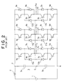
- Fig. 2 is a circuit diagram showing the arrangement of another conventional three-phase, three-level inverter presented, for example, in "A Current Control Scheme for Neutral-Point-clamped Voltage Source Inverters for Vector Control Systems", Thesis No. 113, Electrical Society, Industrial Application Department National Conference in 1989.
- the inverter includes a DC voltage source 1, a reactor 2 connected to the positive terminal of the DC voltage source 1, and a capacitor 3, one terminal P thereof being connected to the reactor 2 and the other terminal N thereof being connected to the negative terminal of the DC voltage source 1.
- the capacitor 3 is made up of a pair of capacitors 3a and 3b of the same rating, and a neutral-point terminal O is lead out from the point at which these capacitors are connected.
- the inverter has pairs of transistors 4a-4b, 4c-4d, 5a-5b, 5c-5d, 6a-6b, and 6c-6d, each transistor of each pair being connected in serial.
- the first transistor pair 4a-4b and the second transistor pair 4c-4d, the third transistor pair 5a-Sb and the fourth transistor pair 5c-5d, and the fifth transistor pair 6a-6b and the sixth transistor pair 6c-6d are respectively connected in series. These series circuits are connected in parallel to each other between both of the terminals P and N of the capacitor 3.
- free-wheeling diodes 7a-7d, 8a-8d, and 9a-9d are respectively reversely connected in parallel.
- the cathodes of the first, third, and fifth diodes 10a, 11a, and 12a are respectively connected to the intermediate points of the first, third, and fifth transistor pairs. Each anode of these diodes is connected to the neutral-point terminal O of the capacitor 3.
- the anodes of the second, fourth, and sixth diodes 10b, 11b, 12b are respectively connected to the intermediate points of the second, fourth, and sixth transistor pairs. Each cathode of these diodes is connected to the neutral-point terminal O of the capacitor 3.
- a U-phase output terminal T u is lead out from the connection point of the first transistor pair and the second transistor pair.
- a V-phase output terminal T v is lead out from the connection point of the third transistor pair and the fourth transistor pair.
- a W-phase output terminal T w is lead out from the connection point of the fifth transistor pair and the sixth transistor pair.
- the U phase will be taken as an example.
- the switching state of each of the transistors 4a to 4d of the U phase i.e., the relationship between the on/off mode and the electrical potential of the output terminal T u , is shown in Table 1.
- the output voltage of the DC voltage source 1 is taken to be 2E.
- the electrical potential or voltage of the output terminal T u has three kinds of values corresponding to the terminals P, N, and O of the capacitor 3, the particular value depending upon the switching state of the transistor. This is the reason why the inverter is called a three-level inverter. The same can be said about the V and W phases as has been said above about the U phase.
- a voltage vector instantaneous space voltage vector
- Table 2 summarizes the above relationship and shows the relationships among on/off modes M1 to M27, voltage vectors VO to V18, and the output potentials V u , V v , and V w of each of the output terminals T u , T v , and T w .
- the neutral-point terminal O of the capacitor 3 be primarily at a zero potential. In practice, however, it varies due to a load current I u supplied to the load from the output terminal T u , and so on. A technique for controlling the selection of the on/off mode in order to suppress the amount of this variation has been previously performed.
- M4 and M5 when a voltage vector V1 is output, M4 and M5, for example, can be selected as an on/off mode. Since the connection relationship among the neutral-point terminal O and the output terminal T u differ depending upon the on/off state of each transistor in both of the modes, the influence exerted on the electrical potential of the middle point terminal O by the load current I u will differ in both of the modes. Hence, the mode in which the electrical potential variation of the neutral-point terminal O is smaller is selected.
- the selection of the above-mentioned on/off mode performed in order to suppress the electrical potential variation of the neutral-point terminal O has been determined from a load current vector. That is, a load current vector is computed from the load currents I u , I v , and I w of each phase, and an on/off mode to be selected has been determined from the area of this load current vector.
- An object of the present invention is to provide a method of controlling a three-phase, three-level inverter, which method is capable of easily making the selection of an on/off mode to suppress an electrical potential variation of the neutral-point terminal O of a capacitor without using a complex apparatus.
- a method of controlling a three-phase, three-level inverter is provided as defined in claim 1.
- Fig. 1 is a flowchart showing a series of operations from “Start” to "End” which are performed in a fixed sampling cycle.
- S1 is a step in which a voltage vector required to obtain a desired three-phase AC output is selected, which corresponds to the primary function of the inverter.
- one of the voltage vectors V0 to V18 listed in Table 2 is selected, and a control signal is sent out to each transistor in accordance with the on/off modes M1 to M27 for generating the selected voltage vector.
- step S3 whether or not the electrical potential E c of the neutral-point terminal O of the capacitor 3 falls below a predetermined lower-limit value (Ec *- ⁇ E c ) is determined.
- E c * indicates the electrical potential instruction value of the neutral-point terminal 0, and ⁇ E c indicates an allowable voltage width.
- step S3 If it is determined in step S3 that E c is below a predetermined lower-limit value, it is judged that a charging request is made, and the process proceeds to step S4 where the capacitor 3 is brought into a charged state so that its electrical potential rises. That is, of the two kinds of on/off modes which exist for the same voltage vector, a mode in which an output electrical potential becomes zero for only one phase is tentatively selected. For example, if the case where a voltage vector is V10 is assumed, an on/off mode M17 corresponds to the one to be selected. Thus, the on/off mode M17 is tentatively selected.
- step S5 whether or not the current of the phase in which the output electrical potential is zero is negative, i.e., the current I u of the U phase is negative in the tentatively selected mode M17, is determined. At this point, the direction in which a current flows out to a load is taken to be positive. Therefore, in step S5, whether or not a current is in the direction in which it flows into the capacitor 3, i.e., whether the above-mentioned charging request is satisfied, is determined. If the result of the judgment is negative, it is judged that the charging request is satisfied, and the corresponding mode is actually selected without further action in step S6, then the process is terminated.
- step S7 if it is judged that the electrical potential E c of the neutral-point terminal O is not below the lower-limit value, it is determined in step S7 whether or not this electrical potential E c is above a predetermined upper-limit value (E c * + ⁇ E c ).
- step S9 If it is determined that E c is above the upper-limit value, it is judged that the capacitor 3 is in the discharge request state. After the same mode selection is made in step S8 as in step S4, it is determined in step S9 whether or not the discharge request is satisfied at this time, i.e., whether or not the current of the corresponding phase flows out from the capacitor 3 in the positive direction. If it is the positive direction, the process proceeds to step S6, where the mode which has been tentatively selected is actually selected, and the process is terminated.
- step S5 When it is judged in step S5 that it is not negative, or when it is judged in step S9 that it is not positive, the process proceeds to step S10, where the other mode from among the two kinds of on/off modes is actually selected.
- step S10 the reason why the charge or discharge request is satisfied by the process of step S10 will be explained.
- the output electrical potential of the other two phases except the phases which were taken notice of in step S4 or S8 becomes zero. That is, the output terminals of the above two phases are directly connected to the neutral-point terminal O of the capacitor 3.
- step S7 when it is judged that the electrical potential E c is not above the upper-limit value, the electrical potential E c of the neutral-point terminal O is seen to exist in the allowable range, after all. Any mode may be selected from the viewpoint of voltage variation. Therefore, in step S11, the on/off mode in which variation of on/off states of switching elements, such as transistors, from the previous on/off mode is smaller is actually selected.
- the apparatus of the present invention becomes simple, and operates more reliably and stably.
- the upper-limit value and the lower-limit value of the variation width of the neutral-point terminal O are set in such a way that an allowable voltage width ⁇ E c is added to or subtracted from the electrical potential instruction value E c *.
- These limit values may be set freely as required.
Landscapes
- Engineering & Computer Science (AREA)
- Power Engineering (AREA)
- Inverter Devices (AREA)
Claims (4)
- Verfahren zum Steuern eines Dreiphasen-Dreipunkt-Wechselrichters, wobei eine Vielzahl von Ein/Aus-Betriebsarten nacheinander geschaltet wird, um einen momentanen Raumspannungszeiger (V0 - V18), der aus einer Kombination der elektrischen Potentiale über Anschlüssen (P, N, O) eines Kondensatorpaars (3a, 3b) gebildet ist, zu steuern, wobei der Wechselrichter aufweist: eine Gleichspannungsquelle (1), wobei das Kondensatorpaar (3a, 3b) zwei Anschlüsse (P, N), die mit der Gleichspannungsquelle (1) verbunden sind, und einen Nullpunktanschluß (O) hat, der zwischen den Kondensatoren (3a, 3b) und zwischen den beiden Anschlüssen (P, N) positioniert ist, eine Vielzahl von Schaltelementpaaren (4a-4b, 4c-4d, 5a-5b, 5c-5d, 6a-6b, 6c-6d), die jeweils in Reihe zwischen jeden der beiden Anschlüsse (P, N) und den Nullpunktanschluß (O) geschaltet sind, und drei Ausgangsklemmen (Tu, Tv, Tw) für jede Phase des Wechselrichters, dadurch gekennzeichnet, daß das Verfahren die folgenden Schritte aufweist:a) probeweises Wählen einer Ein/Aus-Betriebsart für den gewünschten Raumspannungszeiger (V0 - V18), durch den das abgegebene elektrische Potential für nur eine der drei Phasen Null ist;b) Beurteilen, ob der Strom der Ausgangsklemme (Tu, Tv, Tw) für diese eine Phase in einer positiven Richtung ist, in der Strom in eine mit der Ausgangsklemme verbundene Last fließt, oder in einer negativen Richtung ist, in der Strom von der Last weg fließt;c) wenn das elektrische Potential des Nullpunktanschlusses (O) des Kondensatorpaars (3a, 3b) über einem vorgegebenen oberen Grenzwert liegt, tatsächliches Wählen der probeweise gewählten Ein/Aus-Betriebsart, wenn die Beurteilung positiv ist, und Wählen einer anderen Ein/Aus-Betriebsart, wenn die Beurteilung negativ ist;oder
d) wenn das elektrische Potential des Nullpunktanschlusses (O) des Kondensatorpaars (3a, 3b) unter einem vorgegebenen unteren Grenzwert liegt, tatsächliches Wählen der probeweise gewählten Ein/Aus-Betriebsart, wenn die Beurteilung negativ ist, und Wählen einer anderen Ein/Aus-Betriebsart, wenn die Beurteilung positiv ist. - Steuerverfahren nach Anspruch 1, wobei, wenn das elektrische Potential des Nullpunktanschlusses (O) des Kondensatorpaars (3a, 3b) zwischen dem vorgegebenen oberen Grenzwert und dem vorgegebenen unteren Grenzwert liegt, das Verfahren ferner den Schritt aufweist: Wählen der Ein/Aus-Betriebsart, in der die Schaltänderung zwischen Ein/Aus-Zuständen der Schaltelementpaare (4a-4b, 4c-4d, 5a-5b, 5c-5d, 6a-6b, 6c-6d) gegenüber der vorher gewählten Ein/Aus-Betriebsart am geringsten ist.
- Steuerverfahren nach Anspruch 1, wobei der obere Grenzwert eine zulässige Spannungsbreite (ΔEc) aufweist, die zu dem elektrischen Potentialwert (E*c) des Nullpunktanschlusses (O) des Kondensatorpaars (3a, 3b) addiert wird.
- Steuerverfahren nach Anspruch 1, wobei der untere Grenzwert eine zulässige Spannungsbreite (ΔEc) aufweist, die von dem elektrischen Potentialwert (E*c) des Nullpunkt-anschlusses (O) des Kondensatorpaars (3a, 3b) subtrahiert wird.
Applications Claiming Priority (2)
| Application Number | Priority Date | Filing Date | Title |
|---|---|---|---|
| JP96707/90 | 1990-04-11 | ||
| JP2096707A JP2526700B2 (ja) | 1990-04-11 | 1990-04-11 | 3相3値レベルインバ―タ |
Publications (3)
| Publication Number | Publication Date |
|---|---|
| EP0451440A2 EP0451440A2 (de) | 1991-10-16 |
| EP0451440A3 EP0451440A3 (en) | 1992-02-12 |
| EP0451440B1 true EP0451440B1 (de) | 1995-11-29 |
Family
ID=14172224
Family Applications (1)
| Application Number | Title | Priority Date | Filing Date |
|---|---|---|---|
| EP91100378A Expired - Lifetime EP0451440B1 (de) | 1990-04-11 | 1991-01-14 | Verfahren zur Steuerung eines Dreiphasen-Dreipunkt-Wechselrichters |
Country Status (5)
| Country | Link |
|---|---|
| US (1) | US5060129A (de) |
| EP (1) | EP0451440B1 (de) |
| JP (1) | JP2526700B2 (de) |
| DE (1) | DE69114890T2 (de) |
| ES (1) | ES2080167T3 (de) |
Families Citing this family (19)
| Publication number | Priority date | Publication date | Assignee | Title |
|---|---|---|---|---|
| JP3102499B2 (ja) * | 1991-02-28 | 2000-10-23 | 株式会社東芝 | 中性点クランプ式電力変換器の制御装置 |
| US5206802A (en) * | 1991-09-17 | 1993-04-27 | Otis Elevator Company | Blanking interval voltage deviation compensator for inverters and converters |
| JP2765315B2 (ja) * | 1991-11-18 | 1998-06-11 | 株式会社日立製作所 | 電力変換装置及びこれを利用した電気車の制御装置 |
| JP2884880B2 (ja) * | 1992-02-12 | 1999-04-19 | 株式会社日立製作所 | 電力変換器の制御装置 |
| JP3229897B2 (ja) * | 1992-04-13 | 2001-11-19 | 三菱電機株式会社 | 3レベル3相インバータ装置 |
| JP3178075B2 (ja) * | 1992-04-23 | 2001-06-18 | 株式会社日立製作所 | 電力変換器の制御装置および電気車の制御装置 |
| AU651034B2 (en) * | 1992-04-24 | 1994-07-07 | Hitachi Limited | Power converter for converting DC voltage into AC phase voltage having three levels of positive, zero and negative voltage |
| JP2814837B2 (ja) * | 1992-06-04 | 1998-10-27 | 株式会社日立製作所 | 電力変換装置 |
| EP0590502B1 (de) * | 1992-10-02 | 1998-01-28 | Hitachi, Ltd. | Wechselrichter für ein elektrisches Betriebsmittel |
| DE4310785C1 (de) * | 1993-03-27 | 1994-06-01 | Licentia Gmbh | Verfahren zur Symmetrierung von Teilspannungen eines Dreistufenwechselrichters |
| JP2888104B2 (ja) * | 1993-09-01 | 1999-05-10 | 株式会社日立製作所 | 電力変換装置 |
| US6058031A (en) * | 1997-10-23 | 2000-05-02 | General Electric Company | Five level high power motor drive converter and control system |
| US5910892A (en) * | 1997-10-23 | 1999-06-08 | General Electric Company | High power motor drive converter system and modulation control |
| US6842354B1 (en) | 2003-08-08 | 2005-01-11 | Rockwell Automation Technologies, Inc. | Capacitor charge balancing technique for a three-level PWM power converter |
| EP1544994B1 (de) * | 2003-12-15 | 2008-05-28 | Abb Research Ltd. | Verbessertes Verfahren zur Symmetrierung eines Gleichspannungskreises einer Umrichterschaltung zur Schaltung von drei Spannungsniveaus |
| KR101525650B1 (ko) * | 2012-02-16 | 2015-06-11 | 삼성전기주식회사 | 짝수-레벨 인버터 및 이의 구동 방법 |
| KR101412875B1 (ko) | 2012-10-04 | 2014-07-02 | 삼성전기주식회사 | 게이트 구동 회로 및 이를 갖는 인버터 |
| RU2556035C1 (ru) * | 2014-07-25 | 2015-07-10 | Федеральное государственное бюджетное образовательное учреждение высшего профессионального образования "Уфимский государственный авиационный технический университет" | Трехфазный инвертор со звеном постоянного тока и способ управления им |
| DE102020200872A1 (de) | 2020-01-24 | 2021-07-29 | Schmidhauser Ag | Stromrichter, Ladesäule und Fahrzeug |
Family Cites Families (3)
| Publication number | Priority date | Publication date | Assignee | Title |
|---|---|---|---|---|
| US4347558A (en) * | 1981-04-02 | 1982-08-31 | Rockwell International Corporation | Voltage balance control for split capacitors in half bridge DC to DC converter |
| US4635177A (en) * | 1984-11-16 | 1987-01-06 | Sundstrand Corporation | Control for a neutral point clamped PWM inverter |
| EP0356547B1 (de) * | 1988-08-30 | 1992-11-04 | Siemens Aktiengesellschaft | Verfahren zum Betrieb eines Dreipunktwechselrichters |
-
1990
- 1990-04-11 JP JP2096707A patent/JP2526700B2/ja not_active Expired - Lifetime
-
1991
- 1991-01-08 US US07/638,814 patent/US5060129A/en not_active Expired - Fee Related
- 1991-01-14 DE DE69114890T patent/DE69114890T2/de not_active Expired - Fee Related
- 1991-01-14 ES ES91100378T patent/ES2080167T3/es not_active Expired - Lifetime
- 1991-01-14 EP EP91100378A patent/EP0451440B1/de not_active Expired - Lifetime
Also Published As
| Publication number | Publication date |
|---|---|
| DE69114890D1 (de) | 1996-01-11 |
| DE69114890T2 (de) | 1996-08-29 |
| EP0451440A2 (de) | 1991-10-16 |
| ES2080167T3 (es) | 1996-02-01 |
| US5060129A (en) | 1991-10-22 |
| JPH03293971A (ja) | 1991-12-25 |
| JP2526700B2 (ja) | 1996-08-21 |
| EP0451440A3 (en) | 1992-02-12 |
Similar Documents
| Publication | Publication Date | Title |
|---|---|---|
| EP0451440B1 (de) | Verfahren zur Steuerung eines Dreiphasen-Dreipunkt-Wechselrichters | |
| EP1261123B1 (de) | Verfahren zur kontrolle des pwm puls | |
| EP0697763B1 (de) | Mehrfach gekoppelter leistungswandler und seine steuerverfahren | |
| US5621628A (en) | Power converter | |
| EP3627684A1 (de) | Stromwandlungsvorrichtung | |
| US11121637B2 (en) | Power conversion device and power conversion system including a power converter capable of converting between alternating-current (AC) power and direct-current (DC) power | |
| EP1411624B1 (de) | Wechselrichter | |
| JP6779424B1 (ja) | 電力変換装置 | |
| EP4012913A1 (de) | Stromumwandlungsvorrichtung | |
| JPH04138068A (ja) | インバータ装置の駆動回路 | |
| CN114600337B (zh) | 不间断电源装置 | |
| EP2677654B1 (de) | Inverterschaltung | |
| US12255544B2 (en) | Power conversion device that performs power conversion between DC circuit and AC circuit | |
| CN109075719B (zh) | 转换器以及使用该转换器的电力转换装置 | |
| JPH0937592A (ja) | 3レベルインバータのpwm制御方法および制御装置 | |
| US6388903B2 (en) | Voltage compensating apparatus and method for 3-phase inverter employing four switches | |
| CN105391308A (zh) | 矩阵变换器、矩阵变换器的控制装置及矩阵变换器的控制方法 | |
| JP2000287453A (ja) | 多重電力変換装置 | |
| JPH03280619A (ja) | パワー素子駆動回路 | |
| JP3010005B2 (ja) | インバータ装置 | |
| US20250317072A1 (en) | Carrier based model predictive control for converter with filter cells | |
| RU2747554C1 (ru) | Универсальный преобразователь постоянного напряжения для питания многоуровневого инвертора напряжения | |
| US20240113639A1 (en) | Power conversion circuit for driving motor and control method thereof | |
| JP2024163675A (ja) | 電力変換装置 | |
| JPH09149657A (ja) | インバータ装置 |
Legal Events
| Date | Code | Title | Description |
|---|---|---|---|
| PUAI | Public reference made under article 153(3) epc to a published international application that has entered the european phase |
Free format text: ORIGINAL CODE: 0009012 |
|
| AK | Designated contracting states |
Kind code of ref document: A2 Designated state(s): CH DE ES LI SE |
|
| PUAL | Search report despatched |
Free format text: ORIGINAL CODE: 0009013 |
|
| AK | Designated contracting states |
Kind code of ref document: A3 Designated state(s): CH DE ES LI SE |
|
| 17P | Request for examination filed |
Effective date: 19920318 |
|
| 17Q | First examination report despatched |
Effective date: 19931022 |
|
| GRAA | (expected) grant |
Free format text: ORIGINAL CODE: 0009210 |
|
| AK | Designated contracting states |
Kind code of ref document: B1 Designated state(s): CH DE ES LI SE |
|
| REF | Corresponds to: |
Ref document number: 69114890 Country of ref document: DE Date of ref document: 19960111 |
|
| PGFP | Annual fee paid to national office [announced via postgrant information from national office to epo] |
Ref country code: SE Payment date: 19960122 Year of fee payment: 6 |
|
| PGFP | Annual fee paid to national office [announced via postgrant information from national office to epo] |
Ref country code: CH Payment date: 19960124 Year of fee payment: 6 |
|
| PGFP | Annual fee paid to national office [announced via postgrant information from national office to epo] |
Ref country code: ES Payment date: 19960131 Year of fee payment: 6 |
|
| REG | Reference to a national code |
Ref country code: ES Ref legal event code: FG2A Ref document number: 2080167 Country of ref document: ES Kind code of ref document: T3 |
|
| REG | Reference to a national code |
Ref country code: CH Ref legal event code: NV Representative=s name: WILLIAM BLANC & CIE CONSEILS EN PROPRIETE INDUSTRI |
|
| PGFP | Annual fee paid to national office [announced via postgrant information from national office to epo] |
Ref country code: DE Payment date: 19960228 Year of fee payment: 6 |
|
| PLBE | No opposition filed within time limit |
Free format text: ORIGINAL CODE: 0009261 |
|
| STAA | Information on the status of an ep patent application or granted ep patent |
Free format text: STATUS: NO OPPOSITION FILED WITHIN TIME LIMIT |
|
| 26N | No opposition filed | ||
| PG25 | Lapsed in a contracting state [announced via postgrant information from national office to epo] |
Ref country code: SE Effective date: 19970115 Ref country code: ES Free format text: LAPSE BECAUSE OF NON-PAYMENT OF DUE FEES Effective date: 19970115 |
|
| PG25 | Lapsed in a contracting state [announced via postgrant information from national office to epo] |
Ref country code: LI Effective date: 19970131 Ref country code: CH Effective date: 19970131 |
|
| REG | Reference to a national code |
Ref country code: CH Ref legal event code: PL |
|
| PG25 | Lapsed in a contracting state [announced via postgrant information from national office to epo] |
Ref country code: DE Effective date: 19971001 |
|
| EUG | Se: european patent has lapsed |
Ref document number: 91100378.8 |
|
| REG | Reference to a national code |
Ref country code: ES Ref legal event code: FD2A Effective date: 19990301 |