EP0450827A1 - Silizium-Photodiode für monolithisch integrierte Schaltungen und Herstellungsverfahren - Google Patents
Silizium-Photodiode für monolithisch integrierte Schaltungen und Herstellungsverfahren Download PDFInfo
- Publication number
- EP0450827A1 EP0450827A1 EP91302594A EP91302594A EP0450827A1 EP 0450827 A1 EP0450827 A1 EP 0450827A1 EP 91302594 A EP91302594 A EP 91302594A EP 91302594 A EP91302594 A EP 91302594A EP 0450827 A1 EP0450827 A1 EP 0450827A1
- Authority
- EP
- European Patent Office
- Prior art keywords
- silicon
- tub
- substrate
- photodiode
- intrinsic
- Prior art date
- Legal status (The legal status is an assumption and is not a legal conclusion. Google has not performed a legal analysis and makes no representation as to the accuracy of the status listed.)
- Granted
Links
- XUIMIQQOPSSXEZ-UHFFFAOYSA-N Silicon Chemical compound [Si] XUIMIQQOPSSXEZ-UHFFFAOYSA-N 0.000 title claims abstract description 45
- 229910052710 silicon Inorganic materials 0.000 title claims abstract description 42
- 239000010703 silicon Substances 0.000 title claims abstract description 42
- 238000000034 method Methods 0.000 title claims abstract description 14
- 239000000758 substrate Substances 0.000 claims abstract description 38
- 230000002093 peripheral effect Effects 0.000 claims abstract description 15
- 229910021421 monocrystalline silicon Inorganic materials 0.000 claims description 3
- 238000000151 deposition Methods 0.000 claims 1
- VYPSYNLAJGMNEJ-UHFFFAOYSA-N Silicium dioxide Chemical compound O=[Si]=O VYPSYNLAJGMNEJ-UHFFFAOYSA-N 0.000 description 6
- 229910003818 SiH2Cl2 Inorganic materials 0.000 description 4
- 230000008021 deposition Effects 0.000 description 4
- 239000012535 impurity Substances 0.000 description 4
- 230000005855 radiation Effects 0.000 description 4
- 238000005516 engineering process Methods 0.000 description 3
- 230000003287 optical effect Effects 0.000 description 3
- 238000005498 polishing Methods 0.000 description 3
- 230000007547 defect Effects 0.000 description 2
- 239000002019 doping agent Substances 0.000 description 2
- 238000005530 etching Methods 0.000 description 2
- 239000000203 mixture Substances 0.000 description 2
- 230000005693 optoelectronics Effects 0.000 description 2
- 229910052814 silicon oxide Inorganic materials 0.000 description 2
- 235000012431 wafers Nutrition 0.000 description 2
- JBRZTFJDHDCESZ-UHFFFAOYSA-N AsGa Chemical compound [As]#[Ga] JBRZTFJDHDCESZ-UHFFFAOYSA-N 0.000 description 1
- 229910001218 Gallium arsenide Inorganic materials 0.000 description 1
- 238000005299 abrasion Methods 0.000 description 1
- 238000010521 absorption reaction Methods 0.000 description 1
- 229910052782 aluminium Inorganic materials 0.000 description 1
- XAGFODPZIPBFFR-UHFFFAOYSA-N aluminium Chemical compound [Al] XAGFODPZIPBFFR-UHFFFAOYSA-N 0.000 description 1
- 239000000969 carrier Substances 0.000 description 1
- 239000008119 colloidal silica Substances 0.000 description 1
- 239000002131 composite material Substances 0.000 description 1
- 238000010586 diagram Methods 0.000 description 1
- 239000000835 fiber Substances 0.000 description 1
- 230000005669 field effect Effects 0.000 description 1
- 239000005350 fused silica glass Substances 0.000 description 1
- 238000005468 ion implantation Methods 0.000 description 1
- 238000002955 isolation Methods 0.000 description 1
- 230000000873 masking effect Effects 0.000 description 1
- 229910052751 metal Inorganic materials 0.000 description 1
- 239000002184 metal Substances 0.000 description 1
- 230000006911 nucleation Effects 0.000 description 1
- 238000010899 nucleation Methods 0.000 description 1
- TWNQGVIAIRXVLR-UHFFFAOYSA-N oxo(oxoalumanyloxy)alumane Chemical compound O=[Al]O[Al]=O TWNQGVIAIRXVLR-UHFFFAOYSA-N 0.000 description 1
- 239000002245 particle Substances 0.000 description 1
- 229910021420 polycrystalline silicon Inorganic materials 0.000 description 1
- 229920000642 polymer Polymers 0.000 description 1
- 229920005591 polysilicon Polymers 0.000 description 1
- 229920002635 polyurethane Polymers 0.000 description 1
- 239000004814 polyurethane Substances 0.000 description 1
- 230000035755 proliferation Effects 0.000 description 1
- 229920006395 saturated elastomer Polymers 0.000 description 1
- 239000004065 semiconductor Substances 0.000 description 1
- 239000002002 slurry Substances 0.000 description 1
Images


Classifications
-
- H—ELECTRICITY
- H01—ELECTRIC ELEMENTS
- H01L—SEMICONDUCTOR DEVICES NOT COVERED BY CLASS H10
- H01L31/00—Semiconductor devices sensitive to infrared radiation, light, electromagnetic radiation of shorter wavelength or corpuscular radiation and specially adapted either for the conversion of the energy of such radiation into electrical energy or for the control of electrical energy by such radiation; Processes or apparatus specially adapted for the manufacture or treatment thereof or of parts thereof; Details thereof
- H01L31/0248—Semiconductor devices sensitive to infrared radiation, light, electromagnetic radiation of shorter wavelength or corpuscular radiation and specially adapted either for the conversion of the energy of such radiation into electrical energy or for the control of electrical energy by such radiation; Processes or apparatus specially adapted for the manufacture or treatment thereof or of parts thereof; Details thereof characterised by their semiconductor bodies
- H01L31/0352—Semiconductor devices sensitive to infrared radiation, light, electromagnetic radiation of shorter wavelength or corpuscular radiation and specially adapted either for the conversion of the energy of such radiation into electrical energy or for the control of electrical energy by such radiation; Processes or apparatus specially adapted for the manufacture or treatment thereof or of parts thereof; Details thereof characterised by their semiconductor bodies characterised by their shape or by the shapes, relative sizes or disposition of the semiconductor regions
- H01L31/035272—Semiconductor devices sensitive to infrared radiation, light, electromagnetic radiation of shorter wavelength or corpuscular radiation and specially adapted either for the conversion of the energy of such radiation into electrical energy or for the control of electrical energy by such radiation; Processes or apparatus specially adapted for the manufacture or treatment thereof or of parts thereof; Details thereof characterised by their semiconductor bodies characterised by their shape or by the shapes, relative sizes or disposition of the semiconductor regions characterised by at least one potential jump barrier or surface barrier
- H01L31/035281—Shape of the body
-
- H—ELECTRICITY
- H01—ELECTRIC ELEMENTS
- H01L—SEMICONDUCTOR DEVICES NOT COVERED BY CLASS H10
- H01L27/00—Devices consisting of a plurality of semiconductor or other solid-state components formed in or on a common substrate
- H01L27/14—Devices consisting of a plurality of semiconductor or other solid-state components formed in or on a common substrate including semiconductor components sensitive to infrared radiation, light, electromagnetic radiation of shorter wavelength or corpuscular radiation and specially adapted either for the conversion of the energy of such radiation into electrical energy or for the control of electrical energy by such radiation
- H01L27/144—Devices controlled by radiation
- H01L27/1443—Devices controlled by radiation with at least one potential jump or surface barrier
-
- Y—GENERAL TAGGING OF NEW TECHNOLOGICAL DEVELOPMENTS; GENERAL TAGGING OF CROSS-SECTIONAL TECHNOLOGIES SPANNING OVER SEVERAL SECTIONS OF THE IPC; TECHNICAL SUBJECTS COVERED BY FORMER USPC CROSS-REFERENCE ART COLLECTIONS [XRACs] AND DIGESTS
- Y02—TECHNOLOGIES OR APPLICATIONS FOR MITIGATION OR ADAPTATION AGAINST CLIMATE CHANGE
- Y02E—REDUCTION OF GREENHOUSE GAS [GHG] EMISSIONS, RELATED TO ENERGY GENERATION, TRANSMISSION OR DISTRIBUTION
- Y02E10/00—Energy generation through renewable energy sources
- Y02E10/50—Photovoltaic [PV] energy
Definitions
- the present invention relates to photodiodes and, more particularly, to an integrated photodiode for silicon monolithic integrated circuits.
- photodiodes With the rapid proliferation of fiber optic communications systems and associated opto-electronic devices, photodiodes have become increasingly important. Information in the form of optical signals is difficult to process. However photodiodes can convert optical signals to electrical signals, and the resulting electrical signals can be efficiently and reliably processed by one of the very large number of compact, complex and inexpensive processing circuits now available in monolithic integrated circuits through silicon VLSI technology.
- a silicon photodiode is provided as set out in the claims.
- FIG. 1 is a flow diagram showing the process steps used to make a monolithic integrated circuit containing an integrated photodiode in accordance with the invention.
- FIG. 2 shows schematic cross sections of a silicon wafer at various steps in the process of FIG. 1.
- FIG. 3 is an enlarged schematic cross section of a typical monolithic integrated circuit containing an integrated photodiode in accordance with the invention.
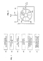
- FIG. 4 is a schematic plan view in elevation of the integrated photodiode of FIG. 3. It is to be understood that these drawings are for purposes of illustrating the concepts of the invention and are not to scale.
- FIG. 1 illustrates the steps in making a monolithically integrated photodiode in accordance with one embodiment of the invention
- FIG. 2 schematically illustrates the structures produced by the successive steps.
- FIG. 1A shows the first step which involves forming a recessed tub in a silicon substrate.
- the upper surface of substrate is provided with etched registration marks and then a masking layer of silicon oxide.
- a deep tub in excess of about 20 microns in depth, is formed in the region of the substrate where the integrated photodiode is to be formed.
- the tub is formed by etching an opening in the oxide mask to define the periphery of the tub (which is typically rectangular) and then etching the tub in the silicon.
- the substrate is (100) oriented silicon with a p-type epitaxial layer on a p+ substrate.
- a preferred etchant is ethylene-diamine-procatechol (EDP). The EDP etch has been found to produce smooth tub surfaces with sidewalls in the (111) planes of the silicon substrate.
- FIG. 2A shows in schematic cross section, the substrate 10, an epitaxial layer 11, the oxide outer layer 12 and tub 13 with smooth side walls 14A and 14B and bottom wall 14C.
- the substrate 10 has p+ resistivity in the range from 0.01 to 0.05 ohm-cm.
- the epitaxial layer 11 has a thickness on the order of 4 microns and p-type conductivity, and the oxide layer 12 conveniently has a thickness of about 3500 angstroms.
- Typical dimensions for the tub are 100x200 microns (at the substrate surface) with a depth of about 30 microns.
- the second step shown in FIG. 1B involves forming a p-n junction around the peripheral surfaces of the tub (side and bottom walls).
- the p-n junction is formed by epitaxially growing thin, doped layers of silicon on the peripheral surfaces.
- the entrenched wafers can be subjected to a combined high temperature pre-bake and HCl - H2 gas etch to reduce native oxide films and to further smooth the bottom and side walls of the tub.
- a five minute prebake and etch at 1025°C using 0.9 l/m of HCl and 40 l/m of H2 is exemplary.
- the p-n junction is then formed as by epitaxially growing doped layers of opposite conductivity type. This growth is preferably effected by lowering the temperature to about 950°C and exposing the substrate to a SiH2Cl2 - HCl - H2 mixture with a 1:1 ratio of HCl to SiH2Cl2 at a pressure of about 40 torr. The deposition rate is approximately 0.10 microns per minute.
- a p-type layer is grown by introducing a gaseous source of p-type impurity into the mixture, and an n-type layer is grown by introducing a gaseous source of n-type impurity.
- the result of the junction-forming step is shown in FIG. 2B.
- the p-type layer 15 and the adjoining n-type layer 16 are disposed on the outer surfaces and on the bottom of tub 13.
- layer 15 is three microns thick and has a concentration of about 3x1015cm ⁇ 3 of p-type impurities.
- Layer 16 is preferably about 1 micron thick and has a concentration of about 7.5x1018cm ⁇ 3 of n-type impurity.
- the next step involves filling the tub with intrinsic silicon by selective epitaxial growth.
- This step is preferably effected by continued exposure of substrate to the SiH2Cl2 - HCl - H2 system without dopants under the conditions described above.
- a deposition temperature of 950°C represents a good compromise between selective growth and a reasonably high growth rate in order to minimize total deposition time.
- the high 1:1 ratio of HCl to SiH2Cl2 reduces growth rates in larger features but also reduces the density of defects.
- the intrinsic semiconductor preferably has an dopant concentration of about 1x1013cm ⁇ 3.
- the resulting structure shown in FIG. 2C has the tub filled with a region of intrinsic silicon 17.
- an observed feature of this structure for deep tubs is a ridge 18 extending around the tub periphery.
- the ridge -- which is not a desired feature -- is believed due to nucleation from the silicon lattice at the edge of the silicon oxide mask.
- the ridge is typically on the order of 20 microns in height.
- the next step shown in FIG. 1D is to planarize the resulting substrate.
- This step involves removing surface irregularities -- including at least portions of ridge 18 -- from the substrate.
- the preferred planarization process is accomplished in two steps.
- the first step is mechanical abrasion by lapping the substrate. Lapping may be done with 1 micron aluminum oxide particles at 60 rpm for 2-4 minutes on a nonmetallic, fused quartz lap.
- the second step is to polish the lapped substrate. Polishing may be effected with a polyurethane polymer pad saturated with colloidal silica slurry.
- the preferred pad is a Suba IV pad marketed by Nalco Chemical Co., Chicago, Illinois, and the preferred silica slurry is Nalco 2350 marketed by the same company. Adequate polishing is effected in 1-2 minutes on a conventional polishing machine.
- the resulting structure shown in schematic cross section is in FIG. 2D.
- the structure comprises substrate 10, a deeply buried p-n junction comprised of layers 15 and 16 of opposite conductivity type, region 17 of intrinsic silicon filling the tub and an outer layer of oxide 19 on a planar surface.
- FIGS. 1E and 1F involve forming a monolithic integrated circuit by conventional means in the region outside the tub region of intrinsic silicon and, preferably at the same time, forming a photodiode within the tub region. Registration with respect to the tub region is provided by the alignment marks etched into the substrate at the beginning of the process.
- FIG. 2E shows only two such components, a pair of CMOS insulated gate field effect transistors 20 and 21 formed outside the tub periphery and connected to a photodiode 22 formed within the tub periphery.
- one of the transistors has its control element (i.e. gate 20G) connected via metal connector 24 to the collecting electrode 25 of photodiode 22 for providing an integrated combination of photodiode and amplifier.
- the photodiode 22, better shown in FIGS. 3 and 4 can be fabricated within the tub periphery separately or at the same time the monolithic integrated circuit is fabricated. The latter approach is preferable.
- contact regions 23, here n+ regions are formed for permitting ohmic contact between electrode 26 and junction layer 16 at the periphery of the tub region.
- a second contact region 29, here p+ is formed in the interior of the tub region, as by ion implantation, for permitting ohmic contact with a collector electrode 25.
- the resulting structure acts as a p-i-n photodiode.
- the photodiode of the invention is monolithically integrated into a substrate of monocrystalline silicon.
- the photodiode comprises a body of epitaxially grown intrinsic silicon disposed within a tub in the substrate.
- the body has the shape of an inverted, truncated pyramid with an upper surface coplanar with the upper surface of the substrate and a thickness (altitude) in excess of about 20 microns.
- An isolation layer in the form of a p-n junction is disposed between the body and the substrate.
- a peripheral electrode 26 extends around the periphery of the body on the upper surface, and a collecting electrode 25 is disposed within the periphery of the body on the upper surface and spaced from the first electrode.
- the substrate is (100) oriented silicon and the side walls of the body are substantially parallel to the (111) planes of the substrate.
- the collecting electrode 25 is spaced from the peripheral electrode 26 by a distance preferably in excess of about 20 microns.
- FIG. 4 is a schematic top plan view of the photodiode in the tub region.
- electrode 26 extends around the periphery of the tub region.
- Collector electrode 25 is in the form of a grid 25 of radial fingers 25A and concentric circles 25B with open areas between to increase the effective area of charge collection while reducing interference with incident radiation.
- the collection electrode grid is spaced away from the periphery of the tub region (and the peripheral electrode 26) with minimum spacing on the order of 20 microns. This minimum spacing is desirable because it has been found by the inventors that most defects in the structure occur near the periphery.
- Conductive connectors 24 and 27 extend from electrodes 25 and 26 to the integrated circuit.
- the peripheral electrode 26 is a composite layer of conductively doped polysilicon (1000 Angstroms) and aluminum (1 micron). It can have a width of about 5 microns.
- the collection electrode 25 is composed of similar elements 25A and 25B having widths of about 5 microns. It is to be understood that the details of the photodiode structure are chosen to be compatible with processing and structure of the adjacent monolithic integrated circuit.
- a voltage of approximately 5-10 volts is applied between electrodes 25 and 26 and the photodiode 22 is exposed to short wave radiation of wavelength between 8000 and 9000 angstroms, as from a gallium arsenide laser or LED (not shown).
- short wave radiation of wavelength between 8000 and 9000 angstroms, as from a gallium arsenide laser or LED (not shown).
- Such radiation when absorbed in the intrinsic layer 17, creates hole-electron pairs which are separated by the field between electrodes 25 and 26.
- One component of the generated pairs is collected by electrode 25.
- the result is that current proportional to the intensity of incident radiation passes through connector 24 to the integrated circuit where it can be amplified by transistor 20 and processed as desired.
- the junction between layers 15 and 16 isolates photodiode 22 in depth so that the operation of the photodiode does not spuriously affect other delicate components in the integrated circuit.
Landscapes
- Physics & Mathematics (AREA)
- Engineering & Computer Science (AREA)
- Power Engineering (AREA)
- Electromagnetism (AREA)
- Condensed Matter Physics & Semiconductors (AREA)
- General Physics & Mathematics (AREA)
- Computer Hardware Design (AREA)
- Microelectronics & Electronic Packaging (AREA)
- Light Receiving Elements (AREA)
Applications Claiming Priority (2)
| Application Number | Priority Date | Filing Date | Title |
|---|---|---|---|
| US07/503,193 US5141878A (en) | 1990-04-02 | 1990-04-02 | Silicon photodiode for monolithic integrated circuits and method for making same |
| US503193 | 1990-04-02 |
Publications (2)
| Publication Number | Publication Date |
|---|---|
| EP0450827A1 true EP0450827A1 (de) | 1991-10-09 |
| EP0450827B1 EP0450827B1 (de) | 1997-05-28 |
Family
ID=24001099
Family Applications (1)
| Application Number | Title | Priority Date | Filing Date |
|---|---|---|---|
| EP91302594A Expired - Lifetime EP0450827B1 (de) | 1990-04-02 | 1991-03-26 | Silizium-Photodiode für monolithisch integrierte Schaltungen und Herstellungsverfahren |
Country Status (4)
| Country | Link |
|---|---|
| US (1) | US5141878A (de) |
| EP (1) | EP0450827B1 (de) |
| JP (1) | JPH04225285A (de) |
| DE (1) | DE69126230T2 (de) |
Cited By (3)
| Publication number | Priority date | Publication date | Assignee | Title |
|---|---|---|---|---|
| EP0917206A1 (de) * | 1997-11-14 | 1999-05-19 | Eastman Kodak Company | CMOS Bildaufnahmevorrichtung |
| GB2386250A (en) * | 2002-03-08 | 2003-09-10 | Denselight Semiconductors Pte | Passive photodetector |
| EP3619555A4 (de) * | 2017-05-03 | 2020-12-16 | Shenzhen Xpectvision Technology Co., Ltd. | Verfahren zur herstellung eines strahlungsdetektors |
Families Citing this family (15)
| Publication number | Priority date | Publication date | Assignee | Title |
|---|---|---|---|---|
| US5494833A (en) * | 1994-07-14 | 1996-02-27 | The United States Of America As Represented By The Secretary Of The Air Force | Backside illuminated MSM device method |
| US5532173A (en) * | 1994-07-14 | 1996-07-02 | The United States Of America As Represented By The Secretary Of The Air Force | FET optical receiver using backside illumination, indium materials species |
| US20070122997A1 (en) | 1998-02-19 | 2007-05-31 | Silicon Genesis Corporation | Controlled process and resulting device |
| US6013563A (en) | 1997-05-12 | 2000-01-11 | Silicon Genesis Corporation | Controlled cleaning process |
| US6287941B1 (en) * | 1999-04-21 | 2001-09-11 | Silicon Genesis Corporation | Surface finishing of SOI substrates using an EPI process |
| US6881644B2 (en) * | 1999-04-21 | 2005-04-19 | Silicon Genesis Corporation | Smoothing method for cleaved films made using a release layer |
| US6171965B1 (en) | 1999-04-21 | 2001-01-09 | Silicon Genesis Corporation | Treatment method of cleaved film for the manufacture of substrates |
| JP4120184B2 (ja) * | 2000-06-30 | 2008-07-16 | セイコーエプソン株式会社 | 実装用微小構造体および光伝送装置 |
| US7542197B2 (en) * | 2003-11-01 | 2009-06-02 | Silicon Quest Kabushiki-Kaisha | Spatial light modulator featured with an anti-reflective structure |
| US8293619B2 (en) | 2008-08-28 | 2012-10-23 | Silicon Genesis Corporation | Layer transfer of films utilizing controlled propagation |
| US8993410B2 (en) | 2006-09-08 | 2015-03-31 | Silicon Genesis Corporation | Substrate cleaving under controlled stress conditions |
| US9362439B2 (en) | 2008-05-07 | 2016-06-07 | Silicon Genesis Corporation | Layer transfer of films utilizing controlled shear region |
| US7811900B2 (en) | 2006-09-08 | 2010-10-12 | Silicon Genesis Corporation | Method and structure for fabricating solar cells using a thick layer transfer process |
| US8330126B2 (en) | 2008-08-25 | 2012-12-11 | Silicon Genesis Corporation | Race track configuration and method for wafering silicon solar substrates |
| US8329557B2 (en) | 2009-05-13 | 2012-12-11 | Silicon Genesis Corporation | Techniques for forming thin films by implantation with reduced channeling |
Citations (3)
| Publication number | Priority date | Publication date | Assignee | Title |
|---|---|---|---|---|
| FR2481519A1 (fr) * | 1979-04-23 | 1981-10-30 | Gen Electric | Dispositif photovoltaique et procede de fabrication |
| EP0067566A2 (de) * | 1981-06-13 | 1982-12-22 | Plessey Overseas Limited | Integrierter Lichtdetektor oder -generator mit Verstärker |
| US4782028A (en) * | 1987-08-27 | 1988-11-01 | Santa Barbara Research Center | Process methodology for two-sided fabrication of devices on thinned silicon |
Family Cites Families (5)
| Publication number | Priority date | Publication date | Assignee | Title |
|---|---|---|---|---|
| JPS61241275A (ja) * | 1985-04-19 | 1986-10-27 | Kayaba Ind Co Ltd | 後輪操舵装置 |
| FR2623664B1 (fr) * | 1987-11-20 | 1990-03-09 | Labo Electronique Physique | Procede de realisation d'un photodetecteur infrarouge integre |
| US4956304A (en) * | 1988-04-07 | 1990-09-11 | Santa Barbara Research Center | Buried junction infrared photodetector process |
| FR2633101B1 (fr) * | 1988-06-16 | 1992-02-07 | Commissariat Energie Atomique | Photodiode et matrice de photodiodes sur hgcdte et leurs procedes de fabrication |
| US5010018A (en) * | 1989-06-21 | 1991-04-23 | General Electric Company | Method for forming Schottky photodiodes |
-
1990
- 1990-04-02 US US07/503,193 patent/US5141878A/en not_active Expired - Lifetime
-
1991
- 1991-03-26 EP EP91302594A patent/EP0450827B1/de not_active Expired - Lifetime
- 1991-03-26 DE DE69126230T patent/DE69126230T2/de not_active Expired - Lifetime
- 1991-04-02 JP JP3068672A patent/JPH04225285A/ja active Pending
Patent Citations (3)
| Publication number | Priority date | Publication date | Assignee | Title |
|---|---|---|---|---|
| FR2481519A1 (fr) * | 1979-04-23 | 1981-10-30 | Gen Electric | Dispositif photovoltaique et procede de fabrication |
| EP0067566A2 (de) * | 1981-06-13 | 1982-12-22 | Plessey Overseas Limited | Integrierter Lichtdetektor oder -generator mit Verstärker |
| US4782028A (en) * | 1987-08-27 | 1988-11-01 | Santa Barbara Research Center | Process methodology for two-sided fabrication of devices on thinned silicon |
Non-Patent Citations (2)
| Title |
|---|
| IEEE TRANSACTIONS ON ELECTRON DEVICES, vol. ED-34, no. 2, February 1987, NEW YORK, US; pages 241 - 246; S. MIURA ET AL.: "A NOVEL PLANARIZATION TECHNIQUE FOR OPTOELECTRONIC INTEGRATED CIRCUITS AND ITS APPLICATION TO A MONOLITHIC AlGaAs/GaAs PIN FET" * |
| PATENT ABSTRACTS OF JAPAN, vol. 10, no. 99 (E-396)[2156] 16 April 1986; & JP-A-60 241 275 (NIPPON DENKI K.K.) 30 November 1985, * |
Cited By (4)
| Publication number | Priority date | Publication date | Assignee | Title |
|---|---|---|---|---|
| EP0917206A1 (de) * | 1997-11-14 | 1999-05-19 | Eastman Kodak Company | CMOS Bildaufnahmevorrichtung |
| US6127697A (en) * | 1997-11-14 | 2000-10-03 | Eastman Kodak Company | CMOS image sensor |
| GB2386250A (en) * | 2002-03-08 | 2003-09-10 | Denselight Semiconductors Pte | Passive photodetector |
| EP3619555A4 (de) * | 2017-05-03 | 2020-12-16 | Shenzhen Xpectvision Technology Co., Ltd. | Verfahren zur herstellung eines strahlungsdetektors |
Also Published As
| Publication number | Publication date |
|---|---|
| US5141878A (en) | 1992-08-25 |
| DE69126230T2 (de) | 1997-12-11 |
| JPH04225285A (ja) | 1992-08-14 |
| DE69126230D1 (de) | 1997-07-03 |
| EP0450827B1 (de) | 1997-05-28 |
Similar Documents
| Publication | Publication Date | Title |
|---|---|---|
| US5239193A (en) | Silicon photodiode for monolithic integrated circuits | |
| US5141878A (en) | Silicon photodiode for monolithic integrated circuits and method for making same | |
| US6458619B1 (en) | Process for producing an isolated planar high speed pin photodiode with improved capacitance | |
| US4814847A (en) | Ingaas semiconductor structures | |
| US5086011A (en) | Process for producing thin single crystal silicon islands on insulator | |
| JPH0287684A (ja) | 集積pin光検出器および方法 | |
| US4794439A (en) | Rear entry photodiode with three contacts | |
| US4148054A (en) | Method of manufacturing a semiconductor device and device manufactured by using the method | |
| US6303967B1 (en) | Process for producing an isolated planar high speed pin photodiode | |
| US4968634A (en) | Fabrication process for photodiodes responsive to blue light | |
| US5279974A (en) | Planar PV HgCdTe DLHJ fabricated by selective cap layer growth | |
| JP2505767B2 (ja) | 光電変換装置の製造方法 | |
| US5106765A (en) | Process for making a bimos | |
| US4920395A (en) | High sensitivity photodiode | |
| US3832246A (en) | Methods for making avalanche diodes | |
| KR920009898B1 (ko) | 수신용 광전집적회로 및 그 제조방법 | |
| US20070272996A1 (en) | Self-aligned implanted waveguide detector | |
| EP0206650B1 (de) | Photoelektrischer Wandler | |
| JP2874570B2 (ja) | 半導体装置およびその製造方法 | |
| US4729963A (en) | Fabrication method for modified planar semiconductor structures | |
| JPS6322474B2 (de) | ||
| CN111129226A (zh) | 锗探测器的制造方法 | |
| CA1078948A (en) | Method of fabricating silicon photodiodes | |
| JPH01503664A (ja) | 被覆層構造物 | |
| US4505765A (en) | Manufacturing method for a planar photodiode with hetero-structure |
Legal Events
| Date | Code | Title | Description |
|---|---|---|---|
| PUAI | Public reference made under article 153(3) epc to a published international application that has entered the european phase |
Free format text: ORIGINAL CODE: 0009012 |
|
| AK | Designated contracting states |
Kind code of ref document: A1 Designated state(s): DE FR GB |
|
| 17P | Request for examination filed |
Effective date: 19920327 |
|
| RAP3 | Party data changed (applicant data changed or rights of an application transferred) |
Owner name: AT&T CORP. |
|
| 17Q | First examination report despatched |
Effective date: 19950120 |
|
| GRAG | Despatch of communication of intention to grant |
Free format text: ORIGINAL CODE: EPIDOS AGRA |
|
| GRAH | Despatch of communication of intention to grant a patent |
Free format text: ORIGINAL CODE: EPIDOS IGRA |
|
| GRAH | Despatch of communication of intention to grant a patent |
Free format text: ORIGINAL CODE: EPIDOS IGRA |
|
| GRAA | (expected) grant |
Free format text: ORIGINAL CODE: 0009210 |
|
| AK | Designated contracting states |
Kind code of ref document: B1 Designated state(s): DE FR GB |
|
| REF | Corresponds to: |
Ref document number: 69126230 Country of ref document: DE Date of ref document: 19970703 |
|
| ET | Fr: translation filed | ||
| K1C1 | Correction of patent application (title page) published |
Effective date: 19911009 |
|
| PLBE | No opposition filed within time limit |
Free format text: ORIGINAL CODE: 0009261 |
|
| STAA | Information on the status of an ep patent application or granted ep patent |
Free format text: STATUS: NO OPPOSITION FILED WITHIN TIME LIMIT |
|
| 26N | No opposition filed | ||
| PGFP | Annual fee paid to national office [announced via postgrant information from national office to epo] |
Ref country code: FR Payment date: 20010222 Year of fee payment: 11 |
|
| REG | Reference to a national code |
Ref country code: GB Ref legal event code: IF02 |
|
| PG25 | Lapsed in a contracting state [announced via postgrant information from national office to epo] |
Ref country code: FR Free format text: LAPSE BECAUSE OF NON-PAYMENT OF DUE FEES Effective date: 20021129 |
|
| REG | Reference to a national code |
Ref country code: FR Ref legal event code: ST |
|
| PGFP | Annual fee paid to national office [announced via postgrant information from national office to epo] |
Ref country code: GB Payment date: 20100322 Year of fee payment: 20 |
|
| PGFP | Annual fee paid to national office [announced via postgrant information from national office to epo] |
Ref country code: DE Payment date: 20100419 Year of fee payment: 20 |
|
| REG | Reference to a national code |
Ref country code: DE Ref legal event code: R071 Ref document number: 69126230 Country of ref document: DE |
|
| REG | Reference to a national code |
Ref country code: GB Ref legal event code: PE20 Expiry date: 20110325 |
|
| PG25 | Lapsed in a contracting state [announced via postgrant information from national office to epo] |
Ref country code: GB Free format text: LAPSE BECAUSE OF EXPIRATION OF PROTECTION Effective date: 20110325 |
|
| PG25 | Lapsed in a contracting state [announced via postgrant information from national office to epo] |
Ref country code: DE Free format text: LAPSE BECAUSE OF EXPIRATION OF PROTECTION Effective date: 20110326 |