EP0447848B1 - Verfahren zum Kalibrieren von Scannern und Anordnung zum Erzeugen definierter Streulichtamplituden - Google Patents
Verfahren zum Kalibrieren von Scannern und Anordnung zum Erzeugen definierter Streulichtamplituden Download PDFInfo
- Publication number
- EP0447848B1 EP0447848B1 EP91102967A EP91102967A EP0447848B1 EP 0447848 B1 EP0447848 B1 EP 0447848B1 EP 91102967 A EP91102967 A EP 91102967A EP 91102967 A EP91102967 A EP 91102967A EP 0447848 B1 EP0447848 B1 EP 0447848B1
- Authority
- EP
- European Patent Office
- Prior art keywords
- reference medium
- light
- photodetector
- scattered
- scattered light
- Prior art date
- Legal status (The legal status is an assumption and is not a legal conclusion. Google has not performed a legal analysis and makes no representation as to the accuracy of the status listed.)
- Expired - Lifetime
Links
- 238000000034 method Methods 0.000 title claims description 21
- 230000003287 optical effect Effects 0.000 claims description 13
- 238000007689 inspection Methods 0.000 claims description 10
- 239000002245 particle Substances 0.000 claims description 10
- 238000005259 measurement Methods 0.000 claims description 9
- 230000007246 mechanism Effects 0.000 claims description 3
- 239000000758 substrate Substances 0.000 claims description 3
- 239000008267 milk Substances 0.000 claims description 2
- 210000004080 milk Anatomy 0.000 claims description 2
- 235000013336 milk Nutrition 0.000 claims description 2
- 239000011521 glass Substances 0.000 claims 1
- 230000001133 acceleration Effects 0.000 description 13
- 235000012431 wafers Nutrition 0.000 description 12
- 230000007547 defect Effects 0.000 description 5
- 230000008569 process Effects 0.000 description 5
- 238000012937 correction Methods 0.000 description 4
- 230000035945 sensitivity Effects 0.000 description 4
- 230000007480 spreading Effects 0.000 description 4
- 230000008859 change Effects 0.000 description 3
- 238000011109 contamination Methods 0.000 description 3
- 238000010586 diagram Methods 0.000 description 3
- 230000003321 amplification Effects 0.000 description 2
- 238000004140 cleaning Methods 0.000 description 2
- 230000001419 dependent effect Effects 0.000 description 2
- 238000000691 measurement method Methods 0.000 description 2
- 238000003199 nucleic acid amplification method Methods 0.000 description 2
- 230000002238 attenuated effect Effects 0.000 description 1
- 230000008901 benefit Effects 0.000 description 1
- 238000012512 characterization method Methods 0.000 description 1
- 239000013078 crystal Substances 0.000 description 1
- 238000009795 derivation Methods 0.000 description 1
- 238000013461 design Methods 0.000 description 1
- 230000003670 easy-to-clean Effects 0.000 description 1
- 239000005338 frosted glass Substances 0.000 description 1
- 238000003384 imaging method Methods 0.000 description 1
- 238000002513 implantation Methods 0.000 description 1
- 239000004816 latex Substances 0.000 description 1
- 229920000126 latex Polymers 0.000 description 1
- 238000012417 linear regression Methods 0.000 description 1
- 230000007935 neutral effect Effects 0.000 description 1
- 230000001151 other effect Effects 0.000 description 1
- 238000012946 outsourcing Methods 0.000 description 1
- 230000003647 oxidation Effects 0.000 description 1
- 238000007254 oxidation reaction Methods 0.000 description 1
- 238000005498 polishing Methods 0.000 description 1
- 230000001105 regulatory effect Effects 0.000 description 1
- 230000003313 weakening effect Effects 0.000 description 1
Images


Classifications
-
- G—PHYSICS
- G01—MEASURING; TESTING
- G01N—INVESTIGATING OR ANALYSING MATERIALS BY DETERMINING THEIR CHEMICAL OR PHYSICAL PROPERTIES
- G01N21/00—Investigating or analysing materials by the use of optical means, i.e. using sub-millimetre waves, infrared, visible or ultraviolet light
- G01N21/84—Systems specially adapted for particular applications
- G01N21/88—Investigating the presence of flaws or contamination
- G01N21/93—Detection standards; Calibrating baseline adjustment, drift correction
-
- G—PHYSICS
- G01—MEASURING; TESTING
- G01N—INVESTIGATING OR ANALYSING MATERIALS BY DETERMINING THEIR CHEMICAL OR PHYSICAL PROPERTIES
- G01N21/00—Investigating or analysing materials by the use of optical means, i.e. using sub-millimetre waves, infrared, visible or ultraviolet light
- G01N21/17—Systems in which incident light is modified in accordance with the properties of the material investigated
- G01N21/47—Scattering, i.e. diffuse reflection
- G01N21/4785—Standardising light scatter apparatus; Standards therefor
Definitions
- the present invention relates to a method for calibration of scanners and an arrangement for generating defined scattered light amplitudes, for measuring particles and surface textures in the inspection of substrate rates, in particular of wafers.
- Devices that are based on the measurement of the elastic scattered light are used, among other things, for the measurement of particles in air or on surfaces or for the inspection of surfaces (US Pat. No. 4,314,763).
- the area to be viewed is illuminated with a high-intensity light source and the scattered light, for example via dark field optics, is fed to a photosensor.
- the photosensor photodiode, photomultiplier
- the photosensor generates an electrical signal that is proportional to the scattered light amplitude and is fed to a subsequent amplifier.
- Such a correction method consists of regular measurements the intensity of the light source. Fluctuations in intensity can then, for example, about changes in sensitivity of the photodetector or the amplifier can be compensated. This However, the correction method has the disadvantage that the changes in optics, in the photodetector or in the amplifier, not recognized and not taken into account.
- the reference medium is, for example, a surface with a very low spreading capacity
- particles, air humidity, oxidation, etc. change its spreading capacity drastically.
- cleaning correspondingly sensitive surfaces is very complex and must be carried out step by step in special cleaning processes. Soiling caused by particles is particularly disadvantageous if the illuminated field is small. In this case, a single particle can change the scattering capacity of the surfaces by orders of magnitude.
- This arrangement therefore covers all possible drift sources. This has the very essential advantage that such an arrangement can work with very low scattered light amplitudes.
- the Arrangement is therefore in terms of sensitivity, accuracy and reliability largely insensitive to contamination and is easy to clean. In addition, such Almost the desired scattered light values over a simply set unlimited range.
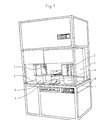
- Fig. 1 shows a substrate surface inspection device as it is mainly used for the inspection of wafers.
- such devices can cause crystal defects, metallic contamination, polishing defects, scratches, Implantation inhomogeneities and other effects visualized on wafers become.
- the necessary purity to carry out such measurements is through a flow box and an aerodynamically transparent design guaranteed.
- FIG. 2 shows a basic illustration of the prior art of a surface inspection device which is based on the principle of measuring the elastic scatter.
- a light source (laser light) 1 illuminates a punctiform spot 2 on a wafer surface 3.
- the reflected light leaves the arrangement in the direction of the arrow.
- a portion 4 of the light scattered from the surface is collected by optics 5 and imaged in a photodetector 7.
- An output signal 8 of the photodetector 7 is fed to an amplifier 9.
- the wafer surface 3 now lies in the so-called focus plane 10. If a defect now occurs at the illuminated point 2, the proportion of the scattered light 4 increases and the intensity of the light reaching the photodetector 7 increases.
- the voltage 11 at the output of the amplifier 9 thus also rises.
- FIG. 3 shows an arrangement of a surface inspection device for generating defined scattered light amplitudes.
- the light emitted by a laser 20 passes through an optical filter 21 (for example an attenuator or a neutral filter) via a beam deflection 22 (for example a mirror or prism) to a converging lens 23.
- This focuses the light to an illuminated spot 24. This lies in the focus plane 10.
- the wafer surface 3 to be inspected lies in the focus plane 10.
- the part 4 of the scattered light scattered by the wafer surface 3 passes through the converging lens 23 and the diaphragm 6 to the photodetector 7.
- the opening 25 of the diaphragm 6 lies in the image 26 of the first illuminated spot 24 (confocal system) and has approximately its shape and dimensions.
- a reference medium 27 is preferably arranged below the focus plane 10. Since the reference medium 27 is thus outside the focus plane 10, a second illuminated spot 28 is larger in terms of extent than the first illuminated spot 24 in the focus plane 10. Likewise, the spot 29 thus illuminated at the aperture 6 is larger in the calibration phase as the image 26. Since the opening 25 of the diaphragm 6 is still the same size, only a very small proportion of the scattered light now reaches the photodetector 7 through the opening 25 of the diaphragm 6.
- a weakening mechanism is thus formed with the aid of the optical filter 21 and / or shifting from the focus plane 10.
- the local stability requirement is eliminated by the outsourcing from the focal plane 10 (defocusing) and the associated enlargement of the illuminated spot 24.
- a scattering reference medium from the volume causes a reference medium 27, the scattering capacity of which is not only limited to the surface 30, but whose volume 31 makes up a substantial part of the scattering capacity (milk, frosted glass) on the one hand defocuses and on the other hand prevents that the spreading behavior can be changed by external influences.
- the setting process takes place according to the following procedure: First, the intensity E1 of the light illuminating the wafer surface 3 is determined. The intensity E2 of the light reaching the photodetector 7 through the opening 25 of the diaphragm 6 is then measured on the reference medium 27 illuminated with E1. The ratio factor, determined from the two intensities E1 and E2, gives the percentage of the proportion of the scattered light from the reference medium 27 that reaches the photodetector 7. The height of the reference medium 27 can now be set so that the desired proportion E0 of scattered light always reaches the photodetector on the reference medium. All surfaces to be inspected are then related to E0. This results in reproducible and stable values for the surface characterization.
- an adjustment mechanism 37 is provided, in which the reference medium 27 - consisting of surface 30 and volume 31 - is arranged on a support 34 which is adjustable in height via an adjusting screw 33.
- the height-adjustable support has an edge 38 which prevents the emission of unwanted scattered light in unwanted directions.
- the height adjustment can be fixed in this embodiment by means of a clamping screw 35. It is also entirely possible to integrate at least one diffractive element 36 (for example a lens) between the light source 20 and the beam deflection 22.
- the lenses described here Laser sources, apertures, optical filters and reference media be built as whole systems and in practice are.
- a lens * there is usually an entire lens system meant the laser in practice is a laser source that comes from two individual sources with different laser light.
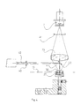
- the representation in FIG. 4 differs from the arrangement shown in FIG. 3 in that the laser light 42 is focused on the wafer surface 3 by a second collecting lens 40, in that the surface 30 of the reference medium 27 lies in the focus plane 10 and that an optical attenuator 41 is provided in the imaging part (between beam deflection 22 and converging lens 23 or between photosensor 7 and converging lens 23) of the scattered portion 4.
- the other consideration elements and considerations are exactly the same as in FIG. 3.
- the circuit section described in FIG. 5a comprises a conventional type of photomultiplier with a first connection 50 to which the negative cathode acceleration voltage Uc can be applied.
- the dynode voltages are tapped via the resistors R1 to Rn, which lie between Uc and ground 51.
- the anode current Ia which is dependent on the light intensity E and the acceleration voltage Uc, is converted into the output voltage Ua by a current-voltage converter.
- 5c shows the relationship between output voltage Ua and acceleration voltage Uc at constant light intensity E.
- the photodetector in the exemplary embodiment described is a photomultiplier, the amplification of which is controlled by the acceleration voltage Uc.
- Uc acceleration voltage
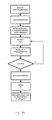
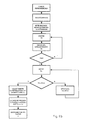
- additional information is required, the derivation of which is determined in the manner in which the flow diagrams can be seen in FIGS. 6a and 6b .
- the photomultiplier is calibrated as far as possible in the sensitivity range in which it is operated during the measurement. In the present arrangement, the intensity reaching the photomultiplier is therefore attenuated by means of an optical filter (attenuator).
- the acceleration voltage is set such that the output voltage Ua is as high as possible without going into the saturation of the amplifier 9.
- the output voltage U1 measured in this way is stored, the attenuator is brought into the beam path, and the voltage U2 is now present at the output of the amplifier.
- Uc EXP (an) where n is the known number of dynodes of the photomultiplier, a and c are unknowns dependent on the photomultiplier. 6b the method is used in detail with which the unknowns are determined in such a way that the gain V can be calculated at each acceleration voltage Uc.
- the output voltage Ua is determined over the entire dynamic range (0 . Umax) of the amplifier 9. This is achieved by gradually increasing the acceleration voltage Uc. After each gradual change in the acceleration voltage Uc, the output voltage Ua is registered.
- the relationship between acceleration voltage Uc and output voltage Ua is according to (2) (3)
- Ua c.
- 5c shows the graphical representation of values determined in the above manner.
- Linear regression can be used to determine m and b from the measured values.
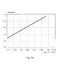
- Fig. 7 shows the relationship between particle size (latex balls) and scattered light intensity. This relationship is the key to determining the size of particles using the scattered light fraction values listed above. This curve only has to be determined once for each machine type.
Landscapes
- Physics & Mathematics (AREA)
- Health & Medical Sciences (AREA)
- Life Sciences & Earth Sciences (AREA)
- Chemical & Material Sciences (AREA)
- Analytical Chemistry (AREA)
- Biochemistry (AREA)
- General Health & Medical Sciences (AREA)
- General Physics & Mathematics (AREA)
- Immunology (AREA)
- Pathology (AREA)
- Investigating Materials By The Use Of Optical Means Adapted For Particular Applications (AREA)
Description
In solchen Geräten wird dabei das zu betrachtende Gebiet mit einer Lichtquelle hoher Intensität beleuchtet und das gestreute Licht -z.B. über eine Dunkelfeldoptik- einem Photosensor zugeführt. Der Photosensor (Photodiode, Photomultiplier) erzeugt ein elektrisches Signal, das proportional zur Streulichtamplitude ist und einem nachfolgenden Verstärker zugeführt wird. Unter der Annahme, dass das Streuvermögen eines Defekts zu dessen Grösse in Relation steht, lassen sich über die Streulichtamplitude Rückschlüsse auf die Ausdehnung des Defekts ziehen.
Aus diesem Grunde wird mittels verschiedener Korrekturmethoden versucht, solche Veränderungen zu kompensieren.
Solche Verfahren verwenden dazu ein Medium von bekanntem Streuvermögen (Referenzmedium) (wie z.B. in US-PS 4,512,659 oder der EP-A-0200918 beschrieben). Ueblicherweise wird dabei auf dem bekannten Medium die Empfindlichkeit vom Photodetektor und vom Verstärker solange verändert, bis der erwünschte Wert am Ausgang des Verstärkers vorliegt, wobei gemäß der EP-A-0200918 mittels eines optischen Abschwächers der Streulichtanteil bestimmt bzw. verändert wird. Bei einem solchen Verfahren hängt damit die Genauigkeit der Kalibrierung noch vom Streuvermögen des Referenzmediums ab.
Zudem ist die Reinigung entsprechend empfindlicher Oberflächen sehr aufwendig und muss in speziellen Reinigungsprozessen schrittweise durchgeführt werden. Besonders nachteilig wirken sich dabei Verschmutzungen durch Partikel aus, wenn das beleuchtete Feld klein ist. In diesem Fall kann ein einzelner Partikel das Streuvermögen der Oberflächen, um Grössenordnungen verändern.
- Fig. 1
- Eine Gesamtdarstellung einer Wafer-Inspektionseinrichtung,in der eine erfindungsgemässe Anordnung zur Anwendung kommt;
- Fig. 2
- eine Prinzipdarstellung des Standes der Technik;
- Fig. 3
- ein Ausführungsbeispiel einer erfindungsgemässen Anordnung;
- Fig. 4
- ein Ausführungsbeispiel ähnlig der EP-A-0200918 zur grundsätzlichen Erläuterung der Anordnung;
- Fig. 5a
- ein Detail-Schaltbild aus dem Ausführungsbeispiel,
- 5b
- eine Photomultiplier-Kennlinie,
- 5c
- eine Ausgangskennlinie bei veränderter Photomultiplier Beschleunigungsspannung;
- Fig. 6a
- ein erstes Flussdiagramm eines Steuerungsablaufs eines automatischen Kalibriervorganges des optischen Filters;
- Fig. 6b
- ein zweites Flussdiagramm eines Steuerungsablaufs eines automatischen Kalibriervorganges zur Ermittlung des Umrechnungsfaktors für die Skalierung der Messresultate;
- Fig. 7
- eine Darstellung des Zusammenhangs zwischen Partikelgrösse und Streulichtintensität.
Diese fokusiert das Licht zu einem beleuchteten Fleck 24. Dieser liegt in der Fokusebene 10. Während des Inspektionsvorganges liegt die zu inspizierende Wafer-Oberfläche 3 in der Fokus-Ebene 10. Der von der Wafer-Oberfläche 3 gestreute Teil 4 des gestreuten Lichtes gelangt durch die Sammellinse 23 und die Blende 6 zum Photodetektor 7. Die Oeffnung 25 der Blende 6 liegt im Abbild 26 des ersten beleuchteten Fleckes 24 (konfokales System) und hat in etwa dessen Form und Abmessungen. Während der Kalibrierphase wird ein Referenzmedium 27 vorzugsweise unterhalb der Fokus-Ebene 10 angeordnet.
Da damit das Referenzmedium 27 ausserhalb der Fokus-Ebene 10 liegt, ist ein zweiter beleuchteter Fleck 28 ausdehnungsmässig grösser als der erste beleuchtete Fleck 24 in der Fokus-Ebene 10. Gleichfalls ist in der Kalibrierphase die so erhellte Stelle 29 am Ort der Blende 6 grösser als das Abbild 26.
Da die Oeffnung 25 der Blende 6 immer noch gleich gross ist, gelangt nunmehr nur ein sehr geringer Anteil des gestreuten Lichtes durch die Oeffnung 25 der Blende 6 zum Photodetektor 7.
Mit Hilfe des optischen Filters 21 und/oder dem Verlagern aus der Fokus-Ebene 10 wird somit ein Abschwächmechanismus gebildet.
Zusätzlich wird durch das Auslagern aus der Fokusebene 10 (Defokusierung) und der damit verbundenen Vergrösserung des beleuchteten Fleckes 24 die örtliche Stabilitätsforderung eliminiert.
Ferner bewirkt ein streuendes Referenzmedium aus dem Volumen -ein Referenzmedium 27, dessen Streuvermögen nicht nur auf die Oberfläche 30 beschränkt ist, sondern dessen Volumen 31 einen wesentlichen Teil des Streuvermögens ausmacht (Milch, Milchglas)-einerseits in sich eine Defokusierung und andererseits verhindert es, dass das Streuverhalten durch äusserliche Einflüsse verändert werden kann.
Durch die Verstellung der Position des Referenzmediums 27 entlang der optischen Achse 32 kann die Grösse der erhellten Stelle 29 an der Stelle der Blende 6 variiert werden.
Bei konstanten Abmessungen der Oeffnung 25 der Blende 6 kann somit die Menge der auf den Photodetektor 7 eintreffenden Energie reguliert werden.
Der Einstellvorgang läuft in der Praxis nach folgendem Procedere ab: Zunächst wird die Intensität E1 des die Wafer-Oberfläche 3 beleuchtenden Lichtes ermittelt. Danach wird auf dem mit E1 beleuchteten Referenzmedium 27 die Intensität E2 des durch die Oeffnung 25 der Blende 6 zum Photodetektor 7 gelangenden Lichtes gemessen. Der Verhältnisfaktor, ermittelt aus den beiden Intensitäten E1 und E2, ergibt den prozentualen Anteil des zum Photodetektor 7 gelangenden Anteils des Streulichtes vom Referenzmedium 27.
Die Höhe des Referenzmediums 27 kann nun so eingestellt werden, dass der gewünschte Anteil E0 an Streulicht stets auf dem Referenzmedium zum Photodetektor gelangt.
Alle zur Inspektion anstehenden Oberflächen werden dann in Relation zu E0 gebracht.
Damit liegen reproduzierbare und stabile Werte für die Oberflächen-Charakterisierung vor.
Die Höheneinstellung lässt sich in diesem Ausführungsbeispiel mittels einer Klemmschraube 35 fixieren.
Es ist im übrigen durchaus möglich zwischen Lichtquelle 20 und Strahlumlenkung 22 wenigstens ein beugendes Element 36 (z.B. eine Linse) zu integrieren.
Die übrigen Betrachtungselemente und Ueberlegungen sind genau gleich wie bei Fig. 3.
Für die Kalibrierung ist es wichtig, dass der Photomultiplier möglichst in dem Empfindlichkeitsbereich geeicht wird, in dem er bei der Messung betrieben wird.
In der vorliegenden Anordnung wird daher mittels eines optischen Filters (Abschwächer) die auf den Photomultiplier gelangende Intensität abgeschwächt.
Fig. 6a zeigt die Ermittlung des Abschwächungsfaktors: Zunächst wird die Beschleunigungsspannung so eingestellt, dass die Ausgangsspannung Ua möglichst hoch ist, ohne in die Sättigung des Verstärkers 9 zu fahren. Die so gemessene Ausgangsspannung U1 wird gespeichert, der Abschwächer wird in den Strahlengang gebracht, und am Ausgang des Verstärkers liegt nunmehr die Spannung U2 an. Das Verhältnis der beiden Spannungen U1 und U2 entspricht dem Abschwächungsfaktor cA des optischen Filters.
Fig. 6b wird im Detail das Verfahren angewendet, mit dem die Unbekannten so bestimmt werden, dass die Verstärkung V bei jeder Beschleunigungsspannung Uc errechnet werden kann.
Bei eingefahrenem Abschwächer wird die Ausgangsspannung Ua über den gesamten Dynamikbereich (0.....Umax) des Verstärkers 9 ermittelt. Dies wird durch schrittweises Erhöhen der Beschleunigungsspannung Uc realisiert. Nach jeder schrittweisen Veränderung der Beschleunigungsspannung Uc wird die Ausgangsspannung Ua registriert.
Die Beziehung zwischen Beschleunigungsspannung Uc und Ausgangsspannung Ua ist nach (2)
Aus den nunmehr bestimmten Werten kann ein Faktor z gebildet werden, mit dem eine bestimmte Ausgangsspannung Ua multipliziert wird, um bei einer Beschleunigungsspannung Uc den streuenden Anteil einer beliebigen Wafer-Oberfläche 3 berechnen zu können:
Diese Kurve muss für jede Maschinentype nur einmalig ermittelt werden.
Claims (4)
- Verfahren zum Kalibrieren von Scannern zur Messung von Partikelgrößen und/oder Oberflächenbeschaffenheiten bei der Inspektion von Substraten, wobei Licht von einer Lichtquelle (20) auf ein stark streuendes Referenzmedium (27) mit bekanntem Streuvermögen geleitet wird und von einem Photodetektor (7) erfaßt wird, sowie die Intensität (E1) des das Referenzmedium (27) beleuchtenden Lichtes und die Intensität (E2) des von dem Referenzmedium (27) gestreuten und den Photodetektor (7) erreichenden Streulichtanteils (4) gemessen werden,
dadurch gekennzeichnet, daß
das Sammeln des von dem Referenzmedium (27) gestreuten Lichtanteils (4) mittels eines optischen Sammellinsensystems (23, 6) erfolgt, wobei das Referenzmedium (27) aus der Fokusebene (10) des Sammelsystems (23, 6) verlagert wird, um die lokale Abhängigkeit der Streulichtamplitude zu reduzieren. - Anordnung, insbesondere bei Wafer-Inspektions-Einrichtungen zur Durchführung des Verfahrens nach Anspruch 1, umfassend ein stark streuendes Referenzmedium (27) mit bekanntem Streuvermögen und eine Lichtquelle (20) zur Beleuchtung des Referenzmediums (27), sowie einen Photodetektor (7) zum Erfassen des von dem Referenzmedium (27) gestreuten Lichtanteils (4),
gekennzeichnet durch
Mittel zur Defokusierung des von dem Referenzmedium (27) gestreuten Lichtanteils (4) bezüglich des Photodetektors (7) und ein optisches Sammellinsensystem (23, 6) zur Bündelung des gestreuten Lichtanteils (4) auf den Photodetektor (7) hin, wobei das optische Sammellinsensystem (23, 6) eine Fokusebene (10) und eine Abbildebene (29) aufweist und die Mittel zur Defokusierung einen Verstellmechanismus (37) zur Verlagerung des Referenzmediums (27) aus der Fokusebene (10) des optischen Sammellinsensystems (23, 6) aufweisen. - Anordnung nach Anspruch 2,
dadurch gekennzeichnet, daß
das Referenzmedium (27) Milchglas ist. - Anordnung nach Anspruch 2 oder 3,
dadurch gekennzeichnet, daß
das Referenzmedium (27) ein das Streuvermögen beeinflussendes Volumen (31) besitzt.
Applications Claiming Priority (3)
| Application Number | Priority Date | Filing Date | Title |
|---|---|---|---|
| CH685/90A CH681495A5 (de) | 1990-03-05 | 1990-03-05 | |
| CH685/90 | 1990-03-05 | ||
| CH68590 | 1990-03-05 |
Publications (3)
| Publication Number | Publication Date |
|---|---|
| EP0447848A2 EP0447848A2 (de) | 1991-09-25 |
| EP0447848A3 EP0447848A3 (en) | 1992-07-01 |
| EP0447848B1 true EP0447848B1 (de) | 2002-09-11 |
Family
ID=4192775
Family Applications (1)
| Application Number | Title | Priority Date | Filing Date |
|---|---|---|---|
| EP91102967A Expired - Lifetime EP0447848B1 (de) | 1990-03-05 | 1991-02-27 | Verfahren zum Kalibrieren von Scannern und Anordnung zum Erzeugen definierter Streulichtamplituden |
Country Status (5)
| Country | Link |
|---|---|
| US (1) | US5108176A (de) |
| EP (1) | EP0447848B1 (de) |
| JP (1) | JPH0697210B2 (de) |
| CH (1) | CH681495A5 (de) |
| DE (1) | DE59109241D1 (de) |
Cited By (1)
| Publication number | Priority date | Publication date | Assignee | Title |
|---|---|---|---|---|
| DE102014111242A1 (de) * | 2014-08-07 | 2016-02-11 | RJL Micro & Analytic Bernhard E. Heneka GmbH | Einrichtung für die Restschmutzanalyse im Bereich der Bauteilsauberkeit |
Families Citing this family (21)
| Publication number | Priority date | Publication date | Assignee | Title |
|---|---|---|---|---|
| US5377002A (en) * | 1991-07-20 | 1994-12-27 | Tet Techno Trust Investment Settlement | Apparatus for surface inspections |
| CH685650A5 (de) * | 1991-07-20 | 1995-08-31 | Tencor Instruments | Einrichtung für Oberflächeninspektionen. |
| US5377001A (en) * | 1991-07-20 | 1994-12-27 | Tet Techno Trust Investment Settlement | Apparatus for surface inspection |
| US5359416A (en) * | 1992-10-19 | 1994-10-25 | Thiokol Corporation | System and process for detecting and monitoring surface defects |
| JP2806747B2 (ja) * | 1993-06-21 | 1998-09-30 | 大日本スクリーン製造株式会社 | 顕微測光装置における反射光測定方法 |
| US6271916B1 (en) * | 1994-03-24 | 2001-08-07 | Kla-Tencor Corporation | Process and assembly for non-destructive surface inspections |
| US5712701A (en) * | 1995-03-06 | 1998-01-27 | Ade Optical Systems Corporation | Surface inspection system and method of inspecting surface of workpiece |
| US6118525A (en) | 1995-03-06 | 2000-09-12 | Ade Optical Systems Corporation | Wafer inspection system for distinguishing pits and particles |
| US5831725A (en) * | 1996-10-16 | 1998-11-03 | Atlas Electric Devices Co. | Two-mode surface defect testing system |
| US6075613A (en) * | 1999-02-26 | 2000-06-13 | General Scanning, Inc. | Optical scanner calibration device |
| IL130087A0 (en) | 1999-05-24 | 2000-02-29 | Nova Measuring Instr Ltd | Optical inspection method and system |
| US6538730B2 (en) * | 2001-04-06 | 2003-03-25 | Kla-Tencor Technologies Corporation | Defect detection system |
| US6819844B2 (en) * | 2002-06-20 | 2004-11-16 | The Boeing Company | Fiber-optic based surface spectroscopy |
| US7116413B2 (en) * | 2002-09-13 | 2006-10-03 | Kla-Tencor Corporation | Inspection system for integrated applications |
| DE10323139A1 (de) * | 2003-05-22 | 2004-12-23 | Leica Microsystems Jena Gmbh | Verfahren und Vorrichtung zum Hochauflösenden Fehlerfinden und Klassifizieren |
| DE102006019468B3 (de) * | 2006-04-26 | 2007-08-30 | Siemens Ag | Optischer Sensor und Verfahren zur optischen Inspektion von Oberflächen |
| JP2011058984A (ja) * | 2009-09-11 | 2011-03-24 | Hitachi High-Technologies Corp | 異物検査装置,検査方法及びプログラム |
| US8873596B2 (en) | 2011-07-22 | 2014-10-28 | Kla-Tencor Corporation | Laser with high quality, stable output beam, and long life high conversion efficiency non-linear crystal |
| US9250178B2 (en) | 2011-10-07 | 2016-02-02 | Kla-Tencor Corporation | Passivation of nonlinear optical crystals |
| GB201415783D0 (en) * | 2014-09-05 | 2014-10-22 | Malvern Instr Ltd | Particle characterisation |
| US9419407B2 (en) | 2014-09-25 | 2016-08-16 | Kla-Tencor Corporation | Laser assembly and inspection system using monolithic bandwidth narrowing apparatus |
Citations (1)
| Publication number | Priority date | Publication date | Assignee | Title |
|---|---|---|---|---|
| US4360275A (en) * | 1980-08-11 | 1982-11-23 | Litton Systems Inc. | Device for measurement of optical scattering |
Family Cites Families (6)
| Publication number | Priority date | Publication date | Assignee | Title |
|---|---|---|---|---|
| US4314763A (en) * | 1979-01-04 | 1982-02-09 | Rca Corporation | Defect detection system |
| US4512659A (en) * | 1983-08-10 | 1985-04-23 | Tencor Instruments | Apparatus for calibrating a surface scanner |
| DE3484982D1 (de) * | 1983-11-26 | 1991-10-02 | Toshiba Kawasaki Kk | Apparat zum nachweis von oberflaechenfehlern. |
| US4776693A (en) * | 1984-05-11 | 1988-10-11 | Nippon Kogaku K. K. | Foreign substance inspecting system including a calibration standard |
| US4902131A (en) * | 1985-03-28 | 1990-02-20 | Kabushiki Kaisha Toshiba | Surface inspection method and apparatus therefor |
| JPH0820371B2 (ja) * | 1988-01-21 | 1996-03-04 | 株式会社ニコン | 欠陥検査装置及び欠陥検査方法 |
-
1990
- 1990-03-05 CH CH685/90A patent/CH681495A5/de not_active IP Right Cessation
- 1990-05-21 US US07/527,051 patent/US5108176A/en not_active Expired - Lifetime
-
1991
- 1991-02-27 DE DE59109241T patent/DE59109241D1/de not_active Expired - Lifetime
- 1991-02-27 EP EP91102967A patent/EP0447848B1/de not_active Expired - Lifetime
- 1991-03-04 JP JP3037305A patent/JPH0697210B2/ja not_active Expired - Lifetime
Patent Citations (1)
| Publication number | Priority date | Publication date | Assignee | Title |
|---|---|---|---|---|
| US4360275A (en) * | 1980-08-11 | 1982-11-23 | Litton Systems Inc. | Device for measurement of optical scattering |
Cited By (1)
| Publication number | Priority date | Publication date | Assignee | Title |
|---|---|---|---|---|
| DE102014111242A1 (de) * | 2014-08-07 | 2016-02-11 | RJL Micro & Analytic Bernhard E. Heneka GmbH | Einrichtung für die Restschmutzanalyse im Bereich der Bauteilsauberkeit |
Also Published As
| Publication number | Publication date |
|---|---|
| CH681495A5 (de) | 1993-03-31 |
| DE59109241D1 (de) | 2002-10-17 |
| EP0447848A3 (en) | 1992-07-01 |
| JPH06167456A (ja) | 1994-06-14 |
| US5108176A (en) | 1992-04-28 |
| EP0447848A2 (de) | 1991-09-25 |
| JPH0697210B2 (ja) | 1994-11-30 |
Similar Documents
| Publication | Publication Date | Title |
|---|---|---|
| EP0447848B1 (de) | Verfahren zum Kalibrieren von Scannern und Anordnung zum Erzeugen definierter Streulichtamplituden | |
| DE3151800C2 (de) | Anordnung zum Ermitteln der Lage eines Werkstücks | |
| DE69807096T2 (de) | Sensorvorrichtung | |
| DE2354141C2 (de) | Optisches Meßverfahren zum Untersuchen von Oberflächen und Einrichtung zur Durchführung des Verfahrens | |
| DE2260090A1 (de) | Einrichtung zum messen der rauhigkeit einer oberflaeche | |
| DE2607850A1 (de) | Geraet zum optischen messen des profiles einer oberflaeche | |
| CH654914A5 (de) | Optoelektronisches messverfahren und einrichtung zum bestimmen der oberflaechenguete streuend reflektierender oder transparenter oberflaechen. | |
| EP0116321A2 (de) | Infrarot-Spektrometer | |
| EP0226843A2 (de) | Vorrichtung zur Messung der Haarigkeit eines Garnes | |
| EP0218213B1 (de) | Verfahren und Vorrichtung zur on-line-Messung von Transmission oder Reflexion an bewegten Objekten im Bereich detektierbarer elektromagnetischer Strahlung | |
| CH685519A5 (de) | Verfahren und Einrichtung zur zerstörungsfreien Oberflächen-Inspektion. | |
| DE1548747B1 (de) | Vorrichtung zur Kompensation von Stoereinfluessen im Strahlengang einer foto-elektrischen Abtasteinrichtung | |
| DE102023129662A1 (de) | Ophthalmisches Gerät und Verfahren zum Ausrichten des ophthalmischen Geräts | |
| WO2019042973A1 (de) | Verfahren zum zählen von photonen mittels eines photomultipliers | |
| DE3016812A1 (de) | Lichtabsorptionsmonitor | |
| WO1989001147A1 (fr) | Procede pour le controle qualite d'un objet plat, notamment pour la detection de defauts dans des matieres textiles, et dispositif a cet effet | |
| DE2818789A1 (de) | Dickenmessgeraet | |
| DE3827913C2 (de) | ||
| DE3003333C2 (de) | Vorrichtung zur Messung von Inhomogenitäten des Brechungsindex | |
| DE4031453C2 (de) | Triangulationsmeßverfahren und Gerät zur Durchführung desselben | |
| JPH0718788B2 (ja) | 光学的微粒子測定装置 | |
| DE4210343A1 (de) | Vorrichtung zur optischen Densitometrie | |
| DE2436528C2 (de) | Elektro-optische Scharfstelleinrichtung | |
| EP0304793A2 (de) | Vorrichtung zur Bestimmung der Dicke von Schichtträgern | |
| DE705975C (de) | Vorrichtung mit lichtempfindlicher Zelle zum selbsttaetigen Nachweisen, Messen oder Registrieren von Truebungen |
Legal Events
| Date | Code | Title | Description |
|---|---|---|---|
| PUAI | Public reference made under article 153(3) epc to a published international application that has entered the european phase |
Free format text: ORIGINAL CODE: 0009012 |
|
| AK | Designated contracting states |
Kind code of ref document: A2 Designated state(s): CH DE FR GB IT LI |
|
| RAP1 | Party data changed (applicant data changed or rights of an application transferred) |
Owner name: TET TECHNO TRUST INVESTMENT SETTLEMENT |
|
| PUAL | Search report despatched |
Free format text: ORIGINAL CODE: 0009013 |
|
| AK | Designated contracting states |
Kind code of ref document: A3 Designated state(s): CH DE FR GB IT LI |
|
| 17P | Request for examination filed |
Effective date: 19921111 |
|
| RAP1 | Party data changed (applicant data changed or rights of an application transferred) |
Owner name: TENCOR INSTRUMENTS |
|
| 17Q | First examination report despatched |
Effective date: 19950306 |
|
| GRAG | Despatch of communication of intention to grant |
Free format text: ORIGINAL CODE: EPIDOS AGRA |
|
| GRAG | Despatch of communication of intention to grant |
Free format text: ORIGINAL CODE: EPIDOS AGRA |
|
| GRAH | Despatch of communication of intention to grant a patent |
Free format text: ORIGINAL CODE: EPIDOS IGRA |
|
| GRAH | Despatch of communication of intention to grant a patent |
Free format text: ORIGINAL CODE: EPIDOS IGRA |
|
| GRAA | (expected) grant |
Free format text: ORIGINAL CODE: 0009210 |
|
| AK | Designated contracting states |
Kind code of ref document: B1 Designated state(s): CH DE FR GB IT LI |
|
| PG25 | Lapsed in a contracting state [announced via postgrant information from national office to epo] |
Ref country code: IT Free format text: LAPSE BECAUSE OF FAILURE TO SUBMIT A TRANSLATION OF THE DESCRIPTION OR TO PAY THE FEE WITHIN THE PRE;WARNING: LAPSES OF ITALIAN PATENTS WITH EFFECTIVE DATE BEFORE 2007 MAY HAVE OCCURRED AT ANY TIME BEFORE 2007. THE CORRECT EFFECTIVE DATE MAY BE DIFFERENT FROM THE ONE RECORDED.SCRIBED TIME-LIMIT Effective date: 20020911 |
|
| REG | Reference to a national code |
Ref country code: GB Ref legal event code: FG4D Free format text: NOT ENGLISH |
|
| REG | Reference to a national code |
Ref country code: CH Ref legal event code: EP |
|
| REF | Corresponds to: |
Ref document number: 59109241 Country of ref document: DE Date of ref document: 20021017 |
|
| PG25 | Lapsed in a contracting state [announced via postgrant information from national office to epo] |
Ref country code: LI Free format text: LAPSE BECAUSE OF NON-PAYMENT OF DUE FEES Effective date: 20030228 Ref country code: CH Free format text: LAPSE BECAUSE OF NON-PAYMENT OF DUE FEES Effective date: 20030228 |
|
| GBT | Gb: translation of ep patent filed (gb section 77(6)(a)/1977) |
Effective date: 20030206 |
|
| REG | Reference to a national code |
Ref country code: FR Ref legal event code: RN |
|
| EN | Fr: translation not filed | ||
| REG | Reference to a national code |
Ref country code: FR Ref legal event code: FC |
|
| PLBE | No opposition filed within time limit |
Free format text: ORIGINAL CODE: 0009261 |
|
| STAA | Information on the status of an ep patent application or granted ep patent |
Free format text: STATUS: NO OPPOSITION FILED WITHIN TIME LIMIT |
|
| ET | Fr: translation filed | ||
| 26N | No opposition filed |
Effective date: 20030612 |
|
| REG | Reference to a national code |
Ref country code: CH Ref legal event code: PL |
|
| PGFP | Annual fee paid to national office [announced via postgrant information from national office to epo] |
Ref country code: FR Payment date: 20100303 Year of fee payment: 20 |
|
| PGFP | Annual fee paid to national office [announced via postgrant information from national office to epo] |
Ref country code: DE Payment date: 20100226 Year of fee payment: 20 Ref country code: GB Payment date: 20100224 Year of fee payment: 20 |
|
| REG | Reference to a national code |
Ref country code: DE Ref legal event code: R071 Ref document number: 59109241 Country of ref document: DE |
|
| REG | Reference to a national code |
Ref country code: GB Ref legal event code: PE20 Expiry date: 20110226 |
|
| PG25 | Lapsed in a contracting state [announced via postgrant information from national office to epo] |
Ref country code: GB Free format text: LAPSE BECAUSE OF EXPIRATION OF PROTECTION Effective date: 20110226 |
|
| PG25 | Lapsed in a contracting state [announced via postgrant information from national office to epo] |
Ref country code: DE Free format text: LAPSE BECAUSE OF EXPIRATION OF PROTECTION Effective date: 20110227 |