EP0447840A2 - Compound semiconducteur device manufacturing process and a compound semiconducteur device manufactured by the same - Google Patents
Compound semiconducteur device manufacturing process and a compound semiconducteur device manufactured by the same Download PDFInfo
- Publication number
- EP0447840A2 EP0447840A2 EP91102769A EP91102769A EP0447840A2 EP 0447840 A2 EP0447840 A2 EP 0447840A2 EP 91102769 A EP91102769 A EP 91102769A EP 91102769 A EP91102769 A EP 91102769A EP 0447840 A2 EP0447840 A2 EP 0447840A2
- Authority
- EP
- European Patent Office
- Prior art keywords
- layer
- structural
- opening
- structural layer
- resist pattern
- Prior art date
- Legal status (The legal status is an assumption and is not a legal conclusion. Google has not performed a legal analysis and makes no representation as to the accuracy of the status listed.)
- Granted
Links
Images


Classifications
-
- H—ELECTRICITY
- H10—SEMICONDUCTOR DEVICES; ELECTRIC SOLID-STATE DEVICES NOT OTHERWISE PROVIDED FOR
- H10D—INORGANIC ELECTRIC SEMICONDUCTOR DEVICES
- H10D30/00—Field-effect transistors [FET]
- H10D30/01—Manufacture or treatment
- H10D30/015—Manufacture or treatment of FETs having heterojunction interface channels or heterojunction gate electrodes, e.g. HEMT
-
- H—ELECTRICITY
- H10—SEMICONDUCTOR DEVICES; ELECTRIC SOLID-STATE DEVICES NOT OTHERWISE PROVIDED FOR
- H10D—INORGANIC ELECTRIC SEMICONDUCTOR DEVICES
- H10D30/00—Field-effect transistors [FET]
- H10D30/40—FETs having zero-dimensional [0D], one-dimensional [1D] or two-dimensional [2D] charge carrier gas channels
- H10D30/47—FETs having zero-dimensional [0D], one-dimensional [1D] or two-dimensional [2D] charge carrier gas channels having two-dimensional [2D] charge carrier gas channels, e.g. nanoribbon FETs or high electron mobility transistors [HEMT]
- H10D30/471—High electron mobility transistors [HEMT] or high hole mobility transistors [HHMT]
- H10D30/475—High electron mobility transistors [HEMT] or high hole mobility transistors [HHMT] having wider bandgap layer formed on top of lower bandgap active layer, e.g. undoped barrier HEMTs such as i-AlGaN/GaN HEMTs
- H10D30/4755—High electron mobility transistors [HEMT] or high hole mobility transistors [HHMT] having wider bandgap layer formed on top of lower bandgap active layer, e.g. undoped barrier HEMTs such as i-AlGaN/GaN HEMTs having wide bandgap charge-carrier supplying layers, e.g. modulation doped HEMTs such as n-AlGaAs/GaAs HEMTs
-
- H—ELECTRICITY
- H10—SEMICONDUCTOR DEVICES; ELECTRIC SOLID-STATE DEVICES NOT OTHERWISE PROVIDED FOR
- H10D—INORGANIC ELECTRIC SEMICONDUCTOR DEVICES
- H10D30/00—Field-effect transistors [FET]
- H10D30/60—Insulated-gate field-effect transistors [IGFET]
- H10D30/67—Thin-film transistors [TFT]
- H10D30/6729—Thin-film transistors [TFT] characterised by the electrodes
- H10D30/6737—Thin-film transistors [TFT] characterised by the electrodes characterised by the electrode materials
- H10D30/6738—Schottky barrier electrodes
-
- H—ELECTRICITY
- H10—SEMICONDUCTOR DEVICES; ELECTRIC SOLID-STATE DEVICES NOT OTHERWISE PROVIDED FOR
- H10D—INORGANIC ELECTRIC SEMICONDUCTOR DEVICES
- H10D30/00—Field-effect transistors [FET]
- H10D30/60—Insulated-gate field-effect transistors [IGFET]
- H10D30/67—Thin-film transistors [TFT]
- H10D30/674—Thin-film transistors [TFT] characterised by the active materials
- H10D30/675—Group III-V materials, Group II-VI materials, Group IV-VI materials, selenium or tellurium
-
- H—ELECTRICITY
- H10—SEMICONDUCTOR DEVICES; ELECTRIC SOLID-STATE DEVICES NOT OTHERWISE PROVIDED FOR
- H10D—INORGANIC ELECTRIC SEMICONDUCTOR DEVICES
- H10D64/00—Electrodes of devices having potential barriers
- H10D64/01—Manufacture or treatment
- H10D64/012—Manufacture or treatment of electrodes comprising a Schottky barrier to a semiconductor
- H10D64/0124—Manufacture or treatment of electrodes comprising a Schottky barrier to a semiconductor to Group III-V semiconductors
- H10D64/0125—Manufacture or treatment of electrodes comprising a Schottky barrier to a semiconductor to Group III-V semiconductors characterised by the sectional shape, e.g. T or inverted T
-
- H—ELECTRICITY
- H10—SEMICONDUCTOR DEVICES; ELECTRIC SOLID-STATE DEVICES NOT OTHERWISE PROVIDED FOR
- H10D—INORGANIC ELECTRIC SEMICONDUCTOR DEVICES
- H10D64/00—Electrodes of devices having potential barriers
- H10D64/60—Electrodes characterised by their materials
- H10D64/64—Electrodes comprising a Schottky barrier to a semiconductor
-
- H—ELECTRICITY
- H10—SEMICONDUCTOR DEVICES; ELECTRIC SOLID-STATE DEVICES NOT OTHERWISE PROVIDED FOR
- H10D—INORGANIC ELECTRIC SEMICONDUCTOR DEVICES
- H10D62/00—Semiconductor bodies, or regions thereof, of devices having potential barriers
- H10D62/80—Semiconductor bodies, or regions thereof, of devices having potential barriers characterised by the materials
- H10D62/85—Semiconductor bodies, or regions thereof, of devices having potential barriers characterised by the materials being Group III-V materials, e.g. GaAs
-
- Y—GENERAL TAGGING OF NEW TECHNOLOGICAL DEVELOPMENTS; GENERAL TAGGING OF CROSS-SECTIONAL TECHNOLOGIES SPANNING OVER SEVERAL SECTIONS OF THE IPC; TECHNICAL SUBJECTS COVERED BY FORMER USPC CROSS-REFERENCE ART COLLECTIONS [XRACs] AND DIGESTS
- Y10—TECHNICAL SUBJECTS COVERED BY FORMER USPC
- Y10S—TECHNICAL SUBJECTS COVERED BY FORMER USPC CROSS-REFERENCE ART COLLECTIONS [XRACs] AND DIGESTS
- Y10S148/00—Metal treatment
- Y10S148/056—Gallium arsenide
-
- Y—GENERAL TAGGING OF NEW TECHNOLOGICAL DEVELOPMENTS; GENERAL TAGGING OF CROSS-SECTIONAL TECHNOLOGIES SPANNING OVER SEVERAL SECTIONS OF THE IPC; TECHNICAL SUBJECTS COVERED BY FORMER USPC CROSS-REFERENCE ART COLLECTIONS [XRACs] AND DIGESTS
- Y10—TECHNICAL SUBJECTS COVERED BY FORMER USPC
- Y10S—TECHNICAL SUBJECTS COVERED BY FORMER USPC CROSS-REFERENCE ART COLLECTIONS [XRACs] AND DIGESTS
- Y10S438/00—Semiconductor device manufacturing: process
- Y10S438/942—Masking
- Y10S438/948—Radiation resist
- Y10S438/951—Lift-off
Definitions
- This invention relates to a process for fabricating compound semiconductor devices. More particularly, this invention relates to a process for fabricating compound semiconductor devices such as high electron mobility transistors (hereinafter referred to simply as "HEMT”) that are suitable for use as low-noise amplifying devices operating in the microwave band.
- HEMT high electron mobility transistors
- a known process for fabricating a HEMT typically comprises the following steps.
- a GaAs buffer (non-doped GaAs) 1 is overlaid successively with an n+-AlGaAs layer 2 and an n+-GaAs layer 3.
- a drain electrode 8 and a source electrode 9 made of a metal establishing an ohmic contact are formed on the n+-GaAs layer 3 by conventional methods.
- the drain electrode 8 and source electrode 9 may be formed by depositing metal by vacuum vapor deposition with a resist pattern having openings being used as a mask.
- the n+-GaAs layer 3 is recessed at later stages to form a drain region 3a and a source region 3b of the HEMT as shown in Fig. 2(f).
- a resist pattern 5 having a reversely tapered opening 4 is formed over the n+-GaAs layer 3 and the electrodes 8 and 9.
- the opening 4 is reversely tapered in order to facilitate the liftoff process in the sixth step to be described later.
- the part of the n+-GaAs layer 3 that is exposed through the opening 4 is subjected to recess-etching, with the resist pattern 5 being used as a mask, whereby the n+-AlGaAs layer 2 is made exposed as shown in Fig. 2(d).
- the recess etching is accomplished by wet etching with a commonly used etchant (e.g. a liquid mixture of H2O2 and H2SO4).
- a gate metal 6 such as Al and W is deposited vertically by vacuum vapor deposition on the area of n+-AlGaAs layer 2 that is exposed through the opening 4, whereby a gate electrode 7 is formed on the n+-AlGaAs layer 2 (see Fig. 2(e)).
- the resist pattern 5 is removed so as to lift off the unwanted gate metal 6, whereby the n-GaAs layer 3 as well as the drain electrode 8 and source electrode 9 formed on that layer are made exposed, thus completing the process of HEMT fabrication (see Fig. 2(f)).
- the distance between the gate electrode 7 and the drain region 3a of the device fabricated by the above process is equal to the distance between the gate electrode 7 and the source region 3b.
- Unexamined Published Japanese Patent Application No. 21877/1988 proposed that the distance between the gate electrode and the drain region be reduced by oblique vacuum vapor deposition of a mask material.
- the position of an opening in the mask is determined by the amount of the oblique deposition, so that it is very difficult to form the gate electrode at a desired position with high precision.
- the most effective way to improve the low noise characteristic of a HEMT is to shorten the gate length, thereby reducing the gate capacitance (C gs ) while increasing the transconductance (g m ). In fact, however, a shorter gate length leads to a greater gate resistance, which may result in a deteriorated low noise characteristic.
- the present invention has been made under these circumstances and has an object of providing a process that is capable of fabricating a compound semiconductor device with the distance between a gate electrode and a source region and that between the gate electrode and a drain region being controlled with high precision.
- Another object of the present invention is to provide a process for fabricating a compound semiconductor device that has a smaller gate resistance and a shorter gate length.
- a process that comprises: the first step of forming successively a first semiconductor layer, a second semiconductor layer for a source and a drain, and a first structural layer on a semiconductor substrate; the second step of forming a first resist pattern with a predetermined opening on the first structural layer; the third step of etching an area of the first structural layer that is exposed through the opening, with the first resist pattern being used as a mask, to thereby make the second semiconductor layer exposed, and thereafter removing the first resist pattern; the fourth step of forming successively a second structural layer and a third structural layer over the exposed area of the second semiconductor layer and the entire first structural layer, the second structural layer being dissoluble by a particular etchant and the third structural layer being less dissoluble than the second structural layer by the etchant; the fifth step of forming on the third structural layer a second resist pattern having an opening that is located over the etched area of the first structural layer and that is distant from an area where a drain is to be formed and close to an area
- a step in which a third resist pattern having an opening larger than the opening formed in the third structural layer by the etching in the sixth step is formed in such a way that the latter opening is positioned within the former opening, is provided between the sixth and seventh steps, and the gate metal to be formed on the first semiconductor layer in the ninth step is vapor-deposited until it is deposited to a height exceeding the third structural layer.
- a gate electrode is to be formed in a position that is closed to a source region and distant from a drain region
- the process of the present invention having the features described above insures that the position of the source region is determined by the source-side edge of the first structural layer formed by the etching in the third step, that the position of the drain region is determined by the drain-side edge of the second structural layer formed by the side etching in the seventh layer, and that the position of the gate electrode is determined by the opening formed in the third structural layer by the etching in the sixth step.
- Figs. 1(a) - 1(k) show the sequence of steps of fabricating a compound semiconductor device according to the embodiment of the present invention.
- the figures depict in cross section the structures that are produced in the individual steps of the process.
- the following description assumes that the semiconductor device to be fabricated is a HEMT, but it should be understood that the process of the present invention is also applicable to other compound semiconductor devices such as low-noise GaAs FETs.
- step (a) a GaAs buffer 11 used as a semiconductor substrate is overlaid in superposition with an n+-AlGaAs layer 12, an n+-GaAs layer 13 for forming a source and a drain, and an insulating SiN layer 14 (see Fig. 1(a)).
- a resist pattern 15 having a predetermined opening 16 is formed over the SiN layer 14 (see Fig. 1(b)).
- the resist pattern 15 is formed by conventional photolithography.
- step (c) the area of SiN layer 14 that is exposed through the opening 16 is etched, with the resist pattern 15 being used as a mask, whereby the corresponding area of the n+-GaAs layer 13 is made exposed. Thereafter, the resist pattern 15 is removed (see Fig. 1(c)).
- the etching may be performed by common wet etching or dry etching technique.
- step (d) a SiON layer 17 and a SiN layer 18 are successively formed over the exposed area of the n+-GaAs layer 13 and the entire SiN layer 14 (see Fig. 1(d)).
- the left side of Fig. 1(e) is the area where a drain is to be formed and the right side is where a source is to be formed.
- the size of the opening 20 corresponds to the "gate length" which is to be discussed later. In other words, the gate length is determined by the opening 20.
- step (f ) the SiON layer 17 and SiN layer 18 are etched, with the resist pattern 19 being used as a mask, whereby the corresponding area of the n+-GaAs layer 13 is made exposed. Thereafter, the resist pattern 19 is removed (see Fig. 1(f)).
- the etching in step (f) is performed by a dry etching technique such as reactive ion etching (RIE) and, therefore, a hole 21 substantially equal in size to the opening 20 can be formed in the SiON layer 17 and the SiN layer 18 by anisotropic etching.
- RIE reactive ion etching
- step (g) a resist pattern 19 having the opening 22 larger than the hole 21 formed in the SiN layer 18 by the etching in step (f) is formed in such a way that the hole 21 is located within the opening 22 (see Fig. 1(g)).
- the size of the opening 22 corresponds to the top size of a gate electrode 27 which is to be discussed later (see Fig. 1(k)).
- the opening 22 is reverse by tapered in order to insure that the resist pattern 19 can be readily lifted off in step (k) to be discussed later.
- step (h) the SiON layer 17 is side-etched with a particular etchant through the hole 21 formed in the SiN layer 18 (see Fig. 1(h)).
- Hydrofluoric acid may be used as this etchant for the side etching. Hydrofluoric acid etches faster a compound that contains many oxygen atoms. Hence, the SiON layer 17 is dissolved by hydrofluoric acid, but the SiN layer 18 is less dissoluble than the SiON layer 17.
- both the SiON layer 17 and SiN layer 18 are made of an insulating material, but this is not necessarily the case of the present invention.
- the structural layers to be combined with the particular etchant may be composed of suitable materials having different solubilities in that etchant.
- a SiO n layer may be used instead of the SiON layer 17.
- the SiN layer 14 is side-etched until the source-side SiN layer 14 becomes exposed, so that the position of the area of the n+-GaAs layer 13 where a source region is to be created is determined with respect to the gate electrode 27 (see Fig. 1(k)).
- step (i) the area of the n+-GaAs layer 13 that is exposed through a hole 21a formed in the SiON layer 17 by the side etching in step (h) is etched to make the n+-AlGaAs layer 12 exposed (see Fig. 1(i)).
- the etching performed in step (i) is recess etching of the same type as performed in the third step of the prior art process shown in Fig. 2(c), and can be accomplished by a known wet etching process.
- a gate metal 26 such as Al and W is vapor-deposited vertically on the n+-AlGaAs layer 12 that is exposed through the hole 21 (see Fig. 1(j)). The metal deposition is continued until the layer of the gate metal 26 is deposited on the n+-AlGaAs layer 12 to a height exceeding the SiN layer 18.
- step (k) the resist pattern 19 (see Fig. 1(j)) is removed to lift off the unwanted layer of the gate metal 26 deposited over the resist pattern 19 (see Fig. 1(k)).
- the resulting gate electrode 27 is larger in the top than in the lower part, and its cross section will be shaped like either T or a mushroom depending upon the size of the hole 21 in the SiN layer 18 and the amount of the gate metal 26 deposited in step (j).
- the gate resistance of the device is small despite the short gate length.
- the gate electrode 27 is formed in such a way that it is supported by the insulating SiN layer 18. Therefore, in order to enhance the mechanical stability of the gate electrode 27, part of the SiN layer 14, SiON layer 17 and SiN layer 18 may be left intact.
- a drain and a source electrode are omitted from the above description, but it should be understood that those electrodes can be formed in the same manner as in the prior art process (see Fig. 2).
- the gate electrode 27 can be positioned distant from a drain region 33a and closer to a source region 33b.
- the position which the gate electrode is to be formed is determined by the hole formed in the third structural layer (i.e., SiN layer 18). Further, the hole in the third structural layer is formed by etching. Hence, the distance between the gate electrode and the source region as well as the distance between the gate electrode and the drain region can be controlled with high precision. Since the gate electrode can be formed at a position that is close to the source region and distant from the drain region, the present invention is capable of fabricating a HEMT of good low-noise characteristic that has a high gate-drain breakdown voltage and a small source resistance.
- the present invention is capable of fabricating a compound semiconductor device that has a small gate resistance and a short gate length and which hence is suitable for use as a HEMT having good low-noise characteristic.
- a first semiconductor layer, a second semiconductor layer for source and drain regions, and a bottom SiN layer are successively formed. After the bottom SiN layer is selectively etched to make an opening, a SiON layer and a top SiN layer are formed thereon. A resist pattern having an opening that is closer to the source region than to the drain region is formed on the top SiN layer. The top SiN layer and SiON layer are etched with the resist pattern used as a mask, to expose the second semiconductor layer. The SiON layer is side-etched with hydrofluoric acid until exposing the gate-side portion of the source-side bottom SiN layer.
- the second semiconductor layer is etched to expose the first semiconductor layer and to form the source and drain regions, where the gate-side edge of the source region is determined by that of the source-side bottom SiN layer and the gate-side edge of the drain region is determined by that of the drain-side SiON layer.
- a gate metal is vapor-deposited vertically on the first semiconductor layer with the opening of the top SiN layer used as a mask.
Landscapes
- Junction Field-Effect Transistors (AREA)
Abstract
Description
- This invention relates to a process for fabricating compound semiconductor devices. More particularly, this invention relates to a process for fabricating compound semiconductor devices such as high electron mobility transistors (hereinafter referred to simply as "HEMT") that are suitable for use as low-noise amplifying devices operating in the microwave band.
- A known process for fabricating a HEMT typically comprises the following steps. In the first step, as shown in Fig. 2a, a GaAs buffer (non-doped GaAs) 1 is overlaid successively with an n⁺-
AlGaAs layer 2 and an n⁺-GaAs layer 3. - In the second step, as shown in Fig. 2(b), a
drain electrode 8 and asource electrode 9 made of a metal establishing an ohmic contact (e.g. AuGe, Ni or Au) are formed on the n⁺-GaAs layer 3 by conventional methods. For example, thedrain electrode 8 andsource electrode 9 may be formed by depositing metal by vacuum vapor deposition with a resist pattern having openings being used as a mask. The n⁺-GaAs layer 3 is recessed at later stages to form adrain region 3a and a source region 3b of the HEMT as shown in Fig. 2(f). - In the third step, as shown in Fig. 2(c), a
resist pattern 5 having a reversely tapered opening 4 is formed over the n⁺-GaAs layer 3 and theelectrodes - In the fourth step, the part of the n⁺-
GaAs layer 3 that is exposed through the opening 4 is subjected to recess-etching, with theresist pattern 5 being used as a mask, whereby the n⁺-AlGaAs layer 2 is made exposed as shown in Fig. 2(d). The recess etching is accomplished by wet etching with a commonly used etchant (e.g. a liquid mixture of H₂O₂ and H₂SO₄). - In the fifth step, with the
resist pattern 5 being used as a mask, agate metal 6 such as Al and W is deposited vertically by vacuum vapor deposition on the area of n⁺-AlGaAs layer 2 that is exposed through the opening 4, whereby agate electrode 7 is formed on the n⁺-AlGaAs layer 2 (see Fig. 2(e)). - In the sixth step, the
resist pattern 5 is removed so as to lift off theunwanted gate metal 6, whereby the n-GaAs layer 3 as well as thedrain electrode 8 andsource electrode 9 formed on that layer are made exposed, thus completing the process of HEMT fabrication (see Fig. 2(f)). - Generally speaking, the smaller the distance between a gate and source, the smaller the source resistance and hence the low noise characteristic of a HEMT is accordingly improved. As shown in Fig. 2(f), the distance between the
gate electrode 7 and thedrain region 3a of the device fabricated by the above process is equal to the distance between thegate electrode 7 and the source region 3b. Hence, if one wants to improve the low noise characteristic of the device by reducing the distance between thegate electrode 7 and the source region 3b, the distance between thegate electrode 7 and thedrain region 3a will inevitably decrease, causing a substantial drop in the breakdown voltage between the gate and drain. - With a view to solving this problem, Unexamined Published Japanese Patent Application No. 21877/1988 proposed that the distance between the gate electrode and the drain region be reduced by oblique vacuum vapor deposition of a mask material. However, according to this method, the position of an opening in the mask is determined by the amount of the oblique deposition, so that it is very difficult to form the gate electrode at a desired position with high precision.
- The most effective way to improve the low noise characteristic of a HEMT is to shorten the gate length, thereby reducing the gate capacitance (Cgs) while increasing the transconductance (gm). In fact, however, a shorter gate length leads to a greater gate resistance, which may result in a deteriorated low noise characteristic.
- The present invention has been made under these circumstances and has an object of providing a process that is capable of fabricating a compound semiconductor device with the distance between a gate electrode and a source region and that between the gate electrode and a drain region being controlled with high precision.
- Another object of the present invention is to provide a process for fabricating a compound semiconductor device that has a smaller gate resistance and a shorter gate length.
- These objects of the present invention can be attained by a process that comprises:
the first step of forming successively a first semiconductor layer, a second semiconductor layer for a source and a drain, and a first structural layer on a semiconductor substrate;
the second step of forming a first resist pattern with a predetermined opening on the first structural layer;
the third step of etching an area of the first structural layer that is exposed through the opening, with the first resist pattern being used as a mask, to thereby make the second semiconductor layer exposed, and thereafter removing the first resist pattern;
the fourth step of forming successively a second structural layer and a third structural layer over the exposed area of the second semiconductor layer and the entire first structural layer, the second structural layer being dissoluble by a particular etchant and the third structural layer being less dissoluble than the second structural layer by the etchant;
the fifth step of forming on the third structural layer a second resist pattern having an opening that is located over the etched area of the first structural layer and that is distant from an area where a drain is to be formed and close to an area where a source is to be formed;
the sixth step of etching the second and third structural layers, with the second resist pattern being used as a mask, so as to make the second semiconductor layer exposed, and thereafter removing the second resist pattern;
the seventh step of side-etching the second structural layer with the above etchant through the opening that has been formed in the third structural layer by the etching in the sixth step;
the eighth step of making the first semiconductor layer exposed by etching an area of the second semiconductor layer that is exposed through a hole that has been formed in the second structural layer by the side etching; and
the ninth step of vapor-depositing a gate metal vertically on the first semiconductor layer that is exposed through the opening formed in the third structural layer. - If desired, a step in which a third resist pattern having an opening larger than the opening formed in the third structural layer by the etching in the sixth step is formed in such a way that the latter opening is positioned within the former opening, is provided between the sixth and seventh steps, and the gate metal to be formed on the first semiconductor layer in the ninth step is vapor-deposited until it is deposited to a height exceeding the third structural layer.
- If a gate electrode is to be formed in a position that is closed to a source region and distant from a drain region, the process of the present invention having the features described above insures that the position of the source region is determined by the source-side edge of the first structural layer formed by the etching in the third step, that the position of the drain region is determined by the drain-side edge of the second structural layer formed by the side etching in the seventh layer, and that the position of the gate electrode is determined by the opening formed in the third structural layer by the etching in the sixth step.
-
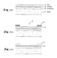
- Figs. 1(a) through 1(k) show the sequence of steps of fabricating a compound semiconductor device according to an embodiment of the present invention; and
- Figs. 2(a) through 2(f) show the sequence of steps of fabricating a compound semiconductor device by a prior art process.
- An embodiment of the present invention is described below in detail with reference to Fig. 1.
- Figs. 1(a) - 1(k) show the sequence of steps of fabricating a compound semiconductor device according to the embodiment of the present invention. The figures depict in cross section the structures that are produced in the individual steps of the process. The following description assumes that the semiconductor device to be fabricated is a HEMT, but it should be understood that the process of the present invention is also applicable to other compound semiconductor devices such as low-noise GaAs FETs.
- The process starts with step (a) in which a
GaAs buffer 11 used as a semiconductor substrate is overlaid in superposition with an n⁺-AlGaAs layer 12, an n⁺-GaAs layer 13 for forming a source and a drain, and an insulating SiN layer 14 (see Fig. 1(a)). - In the next step (b) a
resist pattern 15 having apredetermined opening 16 is formed over the SiN layer 14 (see Fig. 1(b)). In the embodiment under discussion, theresist pattern 15 is formed by conventional photolithography. - In step (c), the area of
SiN layer 14 that is exposed through theopening 16 is etched, with theresist pattern 15 being used as a mask, whereby the corresponding area of the n⁺-GaAs layer 13 is made exposed. Thereafter, theresist pattern 15 is removed (see Fig. 1(c)). The etching may be performed by common wet etching or dry etching technique. - In step (d), a
SiON layer 17 and aSiN layer 18 are successively formed over the exposed area of the n⁺-GaAs layer 13 and the entire SiN layer 14 (see Fig. 1(d)). - In step (e), a
resist pattern 19 having theopening 20 that is located over the etched area (see Fig. 1(c)) of theSiN layer 14 and that is distant from the area where a drain is to be formed and close to the area where a source is to be formed, is formed over the SiN layer 18 (see Fig. 1(e)). The left side of Fig. 1(e) is the area where a drain is to be formed and the right side is where a source is to be formed. The size of the opening 20 corresponds to the "gate length" which is to be discussed later. In other words, the gate length is determined by the opening 20. - In step (f ), the
SiON layer 17 andSiN layer 18 are etched, with theresist pattern 19 being used as a mask, whereby the corresponding area of the n⁺-GaAs layer 13 is made exposed. Thereafter, theresist pattern 19 is removed (see Fig. 1(f)). In the embodiment under discussion, the etching in step (f) is performed by a dry etching technique such as reactive ion etching (RIE) and, therefore, ahole 21 substantially equal in size to theopening 20 can be formed in theSiON layer 17 and theSiN layer 18 by anisotropic etching. - In step (g), a
resist pattern 19 having theopening 22 larger than thehole 21 formed in theSiN layer 18 by the etching in step (f) is formed in such a way that thehole 21 is located within the opening 22 (see Fig. 1(g)). The size of the opening 22 corresponds to the top size of agate electrode 27 which is to be discussed later (see Fig. 1(k)). The opening 22 is reverse by tapered in order to insure that theresist pattern 19 can be readily lifted off in step (k) to be discussed later. - In step (h), the
SiON layer 17 is side-etched with a particular etchant through thehole 21 formed in the SiN layer 18 (see Fig. 1(h)). Hydrofluoric acid may be used as this etchant for the side etching. Hydrofluoric acid etches faster a compound that contains many oxygen atoms. Hence, theSiON layer 17 is dissolved by hydrofluoric acid, but theSiN layer 18 is less dissoluble than theSiON layer 17. In the embodiment, both theSiON layer 17 andSiN layer 18 are made of an insulating material, but this is not necessarily the case of the present invention. The structural layers to be combined with the particular etchant may be composed of suitable materials having different solubilities in that etchant. For example, a SiOn layer may be used instead of theSiON layer 17. In the embodiment, theSiN layer 14 is side-etched until the source-side SiN layer 14 becomes exposed, so that the position of the area of the n⁺-GaAs layer 13 where a source region is to be created is determined with respect to the gate electrode 27 (see Fig. 1(k)). - In step (i), the area of the n⁺-
GaAs layer 13 that is exposed through ahole 21a formed in theSiON layer 17 by the side etching in step (h) is etched to make the n⁺-AlGaAs layer 12 exposed (see Fig. 1(i)). The etching performed in step (i) is recess etching of the same type as performed in the third step of the prior art process shown in Fig. 2(c), and can be accomplished by a known wet etching process. - In step (j), a
gate metal 26 such as Al and W is vapor-deposited vertically on the n⁺-AlGaAs layer 12 that is exposed through the hole 21 (see Fig. 1(j)). The metal deposition is continued until the layer of thegate metal 26 is deposited on the n⁺-AlGaAs layer 12 to a height exceeding theSiN layer 18. - In step (k), the resist pattern 19 (see Fig. 1(j)) is removed to lift off the unwanted layer of the
gate metal 26 deposited over the resist pattern 19 (see Fig. 1(k)). As shown, the resultinggate electrode 27 is larger in the top than in the lower part, and its cross section will be shaped like either T or a mushroom depending upon the size of thehole 21 in theSiN layer 18 and the amount of thegate metal 26 deposited in step (j). Hence, the gate resistance of the device is small despite the short gate length. Thegate electrode 27 is formed in such a way that it is supported by the insulatingSiN layer 18. Therefore, in order to enhance the mechanical stability of thegate electrode 27, part of theSiN layer 14,SiON layer 17 andSiN layer 18 may be left intact. The steps of forming a drain and a source electrode are omitted from the above description, but it should be understood that those electrodes can be formed in the same manner as in the prior art process (see Fig. 2). As described above, thegate electrode 27 can be positioned distant from a drain region 33a and closer to a source region 33b. - As described on the foregoing pages, according to the invention, the position which the gate electrode is to be formed is determined by the hole formed in the third structural layer (i.e., SiN layer 18). Further, the hole in the third structural layer is formed by etching. Hence, the distance between the gate electrode and the source region as well as the distance between the gate electrode and the drain region can be controlled with high precision. Since the gate electrode can be formed at a position that is close to the source region and distant from the drain region, the present invention is capable of fabricating a HEMT of good low-noise characteristic that has a high gate-drain breakdown voltage and a small source resistance.
- If the gate metal to be formed on the first semiconductor layer (i.e., n⁺-AlGaAs layer 12) is evaporated until it is deposited to a height exceeding the third structural layer, the present invention is capable of fabricating a compound semiconductor device that has a small gate resistance and a short gate length and which hence is suitable for use as a HEMT having good low-noise characteristic.
- A first semiconductor layer, a second semiconductor layer for source and drain regions, and a bottom SiN layer are successively formed. After the bottom SiN layer is selectively etched to make an opening, a SiON layer and a top SiN layer are formed thereon. A resist pattern having an opening that is closer to the source region than to the drain region is formed on the top SiN layer. The top SiN layer and SiON layer are etched with the resist pattern used as a mask, to expose the second semiconductor layer. The SiON layer is side-etched with hydrofluoric acid until exposing the gate-side portion of the source-side bottom SiN layer. Then, the second semiconductor layer is etched to expose the first semiconductor layer and to form the source and drain regions, where the gate-side edge of the source region is determined by that of the source-side bottom SiN layer and the gate-side edge of the drain region is determined by that of the drain-side SiON layer. Finally, a gate metal is vapor-deposited vertically on the first semiconductor layer with the opening of the top SiN layer used as a mask.
Claims (12)
- A manufacturing process of a compound semiconductor device, comprising:
the first step of forming successively a first compound semiconductor layer, a second compound semiconductor layer for a source and a drain region, and a first structural layer on a semiconductor substrate;
the second step of forming a first resist pattern having a first opening on the first structural layer;
the third step of etching an area of the first structural layer that is exposed through the first opening with the first resist pattern being used as a mask to thereby expose the second semiconductor layer, and thereafter removing the first resist pattern;
the fourth step of forming successively a second structural layer and a third structural layer on the exposed area of the second semiconductor layer and the entire first structural layer, the second structural layer being dissoluble by a particular etchant and the third structural layer being less dissoluble by the particular etchant than the second structural layer;
the fifth step of forming on the third structural layer a second resist pattern having a second opening that is located over the etched area of the first structural layer and closer to the source region than to the drain region;
the sixth step of etching the second and third structural layers with the second resist pattern being used as a mask to thereby expose the second semiconductor layer through a third opening of the third structural layer, and thereafter removing the second resist pattern;
the seventh step of side-etching the second structural layer with the particular etchant through the third opening of the third structural layer to produce a fourth opening in the second structural layer;
the eighth step of etching the exposed area of the second semiconductor layer through the fourth opening of the second structural layer to thereby expose the first semiconductor layer and to form the source and drain regions in the second semiconductor layer; and
the ninth step of vapor-depositing a gate metal vertically on the exposed area of the first semiconductor layer. - The process according to claim 1, further comprising, between the sixth and seventh steps, the step of forming on the third structural layer a third resist pattern having a fifth opening so that the third opening of the third structural layer is located within the fifth opening, wherein in the ninth step the gate metal is deposited on the first semiconductor layer to a height exceeding the third structural layer.
- The process according to claim 1, wherein in the sixth step the second and third structural layers are etched by dry etching.
- The process according to claim 1, wherein in the seventh step the second structural layer is further side-etched until the first structural layer of a source side is exposed to thereby provide an asymmetrical structure.
- The process according to claim 4, wherein the first structure layer is less dissoluble by the particular etchant than the second structural layer.
- The process according to claim 5, wherein the particular etchant is hydrofluoric acid, and the first, second and third structural layers are a SiN layer, a SiON layer and a SiN layer, respectively.
- The process according to claim 1, wherein the particular etchant is hydrofluoric acid, and the second and third structural layers are a SiON layer and a SiN layer, respectively.
- A compound semiconductor device comprising:
a compound semiconductor layer;
a source region and a drain region formed on the compound semiconductor layer;
a gate electrode having a vertical lower portion and a top portion which is larger in volume than the lower portion, and formed on the compound semiconductor layer and located closer to the source region than to the drain region;
a structural layer formed on the source and drain regions, penetrated by the gate electrode, and supporting the top portion of the gate electrode from below. - The device according to claim 8, wherein the structural layer includes a first layer supporting the top portion of the gate electrode and a second layer placed under the first layer, and the second layer is dissoluble by a particular etchant and the first layer is less dissoluble by the particular etchant than the second layer.
- The device according to claim 9, wherein the structural layer further includes a third layer under the second layer, which is less dissoluble by the particular etchant than the second layer.
- The device according to claim 10, wherein the particular etchant is hydrofluoric acid, and the first, second and third layers are a SiN layer, a SiON layer and a SiN layer, respectively.
- The device according to claim 10, wherein a gate-side edge of the source region is determined by that of the third structural layer and a gate-side edge of the drain region is determined by that of the second layer.
Applications Claiming Priority (3)
| Application Number | Priority Date | Filing Date | Title |
|---|---|---|---|
| JP4522590 | 1990-02-26 | ||
| JP45225/90 | 1990-02-26 | ||
| JP2045225A JPH03248439A (en) | 1990-02-26 | 1990-02-26 | Manufacture of compound semiconductor device |
Publications (3)
| Publication Number | Publication Date |
|---|---|
| EP0447840A2 true EP0447840A2 (en) | 1991-09-25 |
| EP0447840A3 EP0447840A3 (en) | 1995-08-16 |
| EP0447840B1 EP0447840B1 (en) | 2000-07-12 |
Family
ID=12713327
Family Applications (1)
| Application Number | Title | Priority Date | Filing Date |
|---|---|---|---|
| EP91102769A Expired - Lifetime EP0447840B1 (en) | 1990-02-26 | 1991-02-25 | Compound semiconducteur device manufacturing process and a compound semiconducteur device manufactured by the same |
Country Status (4)
| Country | Link |
|---|---|
| US (2) | US5110751A (en) |
| EP (1) | EP0447840B1 (en) |
| JP (1) | JPH03248439A (en) |
| DE (1) | DE69132301T2 (en) |
Cited By (2)
| Publication number | Priority date | Publication date | Assignee | Title |
|---|---|---|---|---|
| FR2691013A1 (en) * | 1992-05-07 | 1993-11-12 | Thomson Composants Microondes | Microwave power FET mfr. - by etching asymmetric gate recess in breakdown voltage controlling recess, to give transistors of high power and gain |
| EP0601541A3 (en) * | 1992-12-08 | 1995-02-08 | Sumitomo Electric Industries | Compound semiconductor device and method for its manufacture. |
Families Citing this family (8)
| Publication number | Priority date | Publication date | Assignee | Title |
|---|---|---|---|---|
| JPH03248439A (en) * | 1990-02-26 | 1991-11-06 | Rohm Co Ltd | Manufacture of compound semiconductor device |
| US5272095A (en) * | 1992-03-18 | 1993-12-21 | Research Triangle Institute | Method of manufacturing heterojunction transistors with self-aligned metal contacts |
| EP0592064B1 (en) * | 1992-08-19 | 1998-09-23 | Mitsubishi Denki Kabushiki Kaisha | Method of producing a field effect transistor |
| JP2725592B2 (en) * | 1994-03-30 | 1998-03-11 | 日本電気株式会社 | Method for manufacturing field effect transistor |
| US5384273A (en) * | 1994-04-26 | 1995-01-24 | Motorola Inc. | Method of making a semiconductor device having a short gate length |
| US6232159B1 (en) * | 1998-07-22 | 2001-05-15 | Matsushita Electric Industrial Co., Ltd. | Method for fabricating compound semiconductor device |
| FR3011119B1 (en) * | 2013-09-23 | 2017-09-29 | Commissariat Energie Atomique | METHOD FOR PRODUCING A TRANSISTOR |
| CN116313790B (en) * | 2023-02-27 | 2025-11-21 | 电子科技大学 | Preparation method of wafer-level nano air channel transistor based on dip angle deposition |
Family Cites Families (31)
| Publication number | Priority date | Publication date | Assignee | Title |
|---|---|---|---|---|
| JPS5921193B2 (en) * | 1977-06-03 | 1984-05-18 | 富士通株式会社 | Method for manufacturing field effect transistors |
| JPH0237755B2 (en) * | 1982-07-27 | 1990-08-27 | Daizen Sogyo Kk | FUKAKANSHISEIGYOSOCHI |
| JPS59193069A (en) * | 1983-04-15 | 1984-11-01 | Nec Corp | Manufacturing method of semiconductor device |
| JPS604268A (en) * | 1983-06-22 | 1985-01-10 | Nec Corp | semiconductor equipment |
| JPS60145669A (en) * | 1984-01-09 | 1985-08-01 | Nec Corp | Gaas fet |
| JPS6155969A (en) * | 1984-08-27 | 1986-03-20 | Nec Corp | Semiconductor device and its manufacturing method |
| US4616400A (en) * | 1984-12-21 | 1986-10-14 | Texas Instruments Incorporated | Process for fabricating a double recess channel field effect transistor |
| JPS61156887A (en) * | 1984-12-28 | 1986-07-16 | Fujitsu Ltd | Manufacture of fet |
| US4656076A (en) * | 1985-04-26 | 1987-04-07 | Triquint Semiconductors, Inc. | Self-aligned recessed gate process |
| JPS625667A (en) * | 1985-07-01 | 1987-01-12 | Nec Corp | Manufacture of semiconductor device |
| JPS6215861A (en) * | 1985-07-12 | 1987-01-24 | Matsushita Electric Ind Co Ltd | Manufacture of semiconductor device |
| JPS62186568A (en) * | 1986-02-12 | 1987-08-14 | Fujitsu Ltd | Manufacture of semiconductor device |
| JPS62232971A (en) * | 1986-04-03 | 1987-10-13 | Nec Corp | Manufacture of semiconductor transistor |
| JPS62250674A (en) * | 1986-04-23 | 1987-10-31 | Nec Corp | Manufactire of semiconductor device |
| JPS6321877A (en) * | 1986-07-16 | 1988-01-29 | Oki Electric Ind Co Ltd | Manufacture of semiconductor element |
| JPS63155671A (en) * | 1986-12-18 | 1988-06-28 | Nec Corp | Manufacture of semiconductor device |
| JPS63208278A (en) * | 1987-02-25 | 1988-08-29 | Oki Electric Ind Co Ltd | Manufacture of field effect transistor |
| JPS63208275A (en) * | 1987-02-25 | 1988-08-29 | Hitachi Ltd | field effect transistor |
| JPS63228761A (en) * | 1987-03-18 | 1988-09-22 | Fujitsu Ltd | Manufacture of semiconductor device |
| JPS63305566A (en) * | 1987-06-05 | 1988-12-13 | Nippon Telegr & Teleph Corp <Ntt> | Semiconductor device and manufacture thereof |
| JP2610435B2 (en) * | 1987-06-29 | 1997-05-14 | ヤンマー農機株式会社 | Combine |
| JPS647664A (en) * | 1987-06-30 | 1989-01-11 | Toshiba Corp | Manufacture of field-effect transistor |
| KR920009718B1 (en) * | 1987-08-10 | 1992-10-22 | 스미도모덴기고오교오 가부시기가이샤 | Compound Semiconductor Device and Manufacturing Method Thereof |
| JPS6446985A (en) * | 1987-08-17 | 1989-02-21 | Mitsubishi Electric Corp | Manufacture of semiconductor device |
| JPH0218942A (en) * | 1988-07-07 | 1990-01-23 | Sumitomo Electric Ind Ltd | Electric field effect transistor and its manufacture |
| KR910005400B1 (en) * | 1988-09-05 | 1991-07-29 | 재단법인 한국전자통신연구소 | Method of manufacturing self-aligned gallium arsenide field effect transistor using multilayer resist |
| JPH0279437A (en) * | 1988-09-14 | 1990-03-20 | Mitsubishi Electric Corp | Manufacture of semiconductor device |
| JPH02140942A (en) * | 1988-11-22 | 1990-05-30 | Matsushita Electric Ind Co Ltd | Manufacture of semiconductor device |
| JPH0355852A (en) * | 1989-07-25 | 1991-03-11 | Sony Corp | Manufacture of semiconductor device |
| US4963501A (en) * | 1989-09-25 | 1990-10-16 | Rockwell International Corporation | Method of fabricating semiconductor devices with sub-micron linewidths |
| JPH03248439A (en) * | 1990-02-26 | 1991-11-06 | Rohm Co Ltd | Manufacture of compound semiconductor device |
-
1990
- 1990-02-26 JP JP2045225A patent/JPH03248439A/en active Pending
-
1991
- 1991-02-20 US US07/658,218 patent/US5110751A/en not_active Expired - Lifetime
- 1991-02-25 EP EP91102769A patent/EP0447840B1/en not_active Expired - Lifetime
- 1991-02-25 DE DE69132301T patent/DE69132301T2/en not_active Expired - Fee Related
-
1993
- 1993-02-24 US US08/023,151 patent/US5296728A/en not_active Expired - Fee Related
Cited By (2)
| Publication number | Priority date | Publication date | Assignee | Title |
|---|---|---|---|---|
| FR2691013A1 (en) * | 1992-05-07 | 1993-11-12 | Thomson Composants Microondes | Microwave power FET mfr. - by etching asymmetric gate recess in breakdown voltage controlling recess, to give transistors of high power and gain |
| EP0601541A3 (en) * | 1992-12-08 | 1995-02-08 | Sumitomo Electric Industries | Compound semiconductor device and method for its manufacture. |
Also Published As
| Publication number | Publication date |
|---|---|
| EP0447840A3 (en) | 1995-08-16 |
| DE69132301T2 (en) | 2001-01-18 |
| US5110751A (en) | 1992-05-05 |
| DE69132301D1 (en) | 2000-08-17 |
| JPH03248439A (en) | 1991-11-06 |
| EP0447840B1 (en) | 2000-07-12 |
| US5296728A (en) | 1994-03-22 |
Similar Documents
| Publication | Publication Date | Title |
|---|---|---|
| US5288654A (en) | Method of making a mushroom-shaped gate electrode of semiconductor device | |
| US5399896A (en) | FET with a T-shaped gate of a particular structure | |
| US5110751A (en) | Method of manufacturing a compound semiconductor device | |
| US5550065A (en) | Method of fabricating self-aligned FET structure having a high temperature stable T-shaped Schottky gate contact | |
| KR100647459B1 (en) | Method for manufacturing tee or gamma gate electrode | |
| US5231040A (en) | Method of making a field effect transistor | |
| JPH05326563A (en) | Semiconductor device | |
| US5719088A (en) | Method of fabricating semiconductor devices with a passivated surface | |
| GB2286720A (en) | Field effect transistors | |
| JP3144089B2 (en) | Method for manufacturing field effect transistor | |
| EP0394590A2 (en) | Field effect transistors and method of making a field effect transistor | |
| JPS61156887A (en) | Manufacture of fet | |
| US20080064155A1 (en) | Method for Producing a Multi-Stage Recess in a Layer Structure and a Field Effect Transistor with a Multi-Recessed Gate | |
| EP0552763A2 (en) | Compound semiconductor device with self-aligned gate and method of producing this compound semiconductor device | |
| JPH05218090A (en) | Manufacture of field effect transistor | |
| JP2893776B2 (en) | Method for manufacturing semiconductor device | |
| JPH02142143A (en) | Manufacture of filed effect transistor | |
| JPH01133374A (en) | Manufacture of compound semiconductor field effect transistor | |
| JP3272529B2 (en) | Method of forming recess gate | |
| KR950008264B1 (en) | Making method of gaas fet | |
| JPH04336432A (en) | Field effect transistor | |
| JPH05206169A (en) | Method for manufacturing semiconductor device | |
| JPH02285643A (en) | Manufacture of semiconductor device | |
| JPS616870A (en) | Manufacture of field-effect transistor | |
| JPS62260370A (en) | Field-effect transistor |
Legal Events
| Date | Code | Title | Description |
|---|---|---|---|
| PUAI | Public reference made under article 153(3) epc to a published international application that has entered the european phase |
Free format text: ORIGINAL CODE: 0009012 |
|
| 17P | Request for examination filed |
Effective date: 19910325 |
|
| AK | Designated contracting states |
Kind code of ref document: A2 Designated state(s): DE FR GB |
|
| PUAL | Search report despatched |
Free format text: ORIGINAL CODE: 0009013 |
|
| AK | Designated contracting states |
Kind code of ref document: A3 Designated state(s): DE FR GB |
|
| 17Q | First examination report despatched |
Effective date: 19961105 |
|
| GRAG | Despatch of communication of intention to grant |
Free format text: ORIGINAL CODE: EPIDOS AGRA |
|
| GRAG | Despatch of communication of intention to grant |
Free format text: ORIGINAL CODE: EPIDOS AGRA |
|
| GRAH | Despatch of communication of intention to grant a patent |
Free format text: ORIGINAL CODE: EPIDOS IGRA |
|
| GRAH | Despatch of communication of intention to grant a patent |
Free format text: ORIGINAL CODE: EPIDOS IGRA |
|
| GRAA | (expected) grant |
Free format text: ORIGINAL CODE: 0009210 |
|
| AK | Designated contracting states |
Kind code of ref document: B1 Designated state(s): DE FR GB |
|
| REF | Corresponds to: |
Ref document number: 69132301 Country of ref document: DE Date of ref document: 20000817 |
|
| ET | Fr: translation filed | ||
| PLBE | No opposition filed within time limit |
Free format text: ORIGINAL CODE: 0009261 |
|
| STAA | Information on the status of an ep patent application or granted ep patent |
Free format text: STATUS: NO OPPOSITION FILED WITHIN TIME LIMIT |
|
| 26N | No opposition filed | ||
| REG | Reference to a national code |
Ref country code: GB Ref legal event code: IF02 |
|
| PGFP | Annual fee paid to national office [announced via postgrant information from national office to epo] |
Ref country code: FR Payment date: 20030210 Year of fee payment: 13 |
|
| PGFP | Annual fee paid to national office [announced via postgrant information from national office to epo] |
Ref country code: GB Payment date: 20030219 Year of fee payment: 13 |
|
| PGFP | Annual fee paid to national office [announced via postgrant information from national office to epo] |
Ref country code: DE Payment date: 20030306 Year of fee payment: 13 |
|
| PG25 | Lapsed in a contracting state [announced via postgrant information from national office to epo] |
Ref country code: GB Free format text: LAPSE BECAUSE OF NON-PAYMENT OF DUE FEES Effective date: 20040225 |
|
| PG25 | Lapsed in a contracting state [announced via postgrant information from national office to epo] |
Ref country code: DE Free format text: LAPSE BECAUSE OF NON-PAYMENT OF DUE FEES Effective date: 20040901 |
|
| GBPC | Gb: european patent ceased through non-payment of renewal fee |
Effective date: 20040225 |
|
| PG25 | Lapsed in a contracting state [announced via postgrant information from national office to epo] |
Ref country code: FR Free format text: LAPSE BECAUSE OF NON-PAYMENT OF DUE FEES Effective date: 20041029 |
|
| REG | Reference to a national code |
Ref country code: FR Ref legal event code: ST |