EP0444404B1 - Hochspannungsbrückenschnittstelle für Wechselstrom- und bürstenlose Gleichstrommotor-Steuerung - Google Patents
Hochspannungsbrückenschnittstelle für Wechselstrom- und bürstenlose Gleichstrommotor-Steuerung Download PDFInfo
- Publication number
- EP0444404B1 EP0444404B1 EP91100366A EP91100366A EP0444404B1 EP 0444404 B1 EP0444404 B1 EP 0444404B1 EP 91100366 A EP91100366 A EP 91100366A EP 91100366 A EP91100366 A EP 91100366A EP 0444404 B1 EP0444404 B1 EP 0444404B1
- Authority
- EP
- European Patent Office
- Prior art keywords
- coupled
- transistors
- output
- transistor
- source
- Prior art date
- Legal status (The legal status is an assumption and is not a legal conclusion. Google has not performed a legal analysis and makes no representation as to the accuracy of the status listed.)
- Expired - Lifetime
Links
- 238000002955 isolation Methods 0.000 claims description 13
- 238000000034 method Methods 0.000 claims description 3
- 238000012358 sourcing Methods 0.000 claims description 2
- 239000004020 conductor Substances 0.000 description 13
- 230000010354 integration Effects 0.000 description 8
- 238000004804 winding Methods 0.000 description 8
- 230000036039 immunity Effects 0.000 description 5
- 238000010586 diagram Methods 0.000 description 2
- 238000009877 rendering Methods 0.000 description 2
- 238000000638 solvent extraction Methods 0.000 description 2
- XUIMIQQOPSSXEZ-UHFFFAOYSA-N Silicon Chemical compound [Si] XUIMIQQOPSSXEZ-UHFFFAOYSA-N 0.000 description 1
- 230000005669 field effect Effects 0.000 description 1
- 230000004907 flux Effects 0.000 description 1
- 230000001939 inductive effect Effects 0.000 description 1
- 238000004519 manufacturing process Methods 0.000 description 1
- 239000002184 metal Substances 0.000 description 1
- 229910044991 metal oxide Inorganic materials 0.000 description 1
- 150000004706 metal oxides Chemical class 0.000 description 1
- 210000003205 muscle Anatomy 0.000 description 1
- 230000010363 phase shift Effects 0.000 description 1
- 239000004065 semiconductor Substances 0.000 description 1
- 229910052710 silicon Inorganic materials 0.000 description 1
- 239000010703 silicon Substances 0.000 description 1
- 230000007704 transition Effects 0.000 description 1
Images

Classifications
-
- H—ELECTRICITY
- H02—GENERATION; CONVERSION OR DISTRIBUTION OF ELECTRIC POWER
- H02P—CONTROL OR REGULATION OF ELECTRIC MOTORS, ELECTRIC GENERATORS OR DYNAMO-ELECTRIC CONVERTERS; CONTROLLING TRANSFORMERS, REACTORS OR CHOKE COILS
- H02P1/00—Arrangements for starting electric motors or dynamo-electric converters
-
- H—ELECTRICITY
- H02—GENERATION; CONVERSION OR DISTRIBUTION OF ELECTRIC POWER
- H02M—APPARATUS FOR CONVERSION BETWEEN AC AND AC, BETWEEN AC AND DC, OR BETWEEN DC AND DC, AND FOR USE WITH MAINS OR SIMILAR POWER SUPPLY SYSTEMS; CONVERSION OF DC OR AC INPUT POWER INTO SURGE OUTPUT POWER; CONTROL OR REGULATION THEREOF
- H02M7/00—Conversion of AC power input into DC power output; Conversion of DC power input into AC power output
- H02M7/42—Conversion of DC power input into AC power output without possibility of reversal
- H02M7/44—Conversion of DC power input into AC power output without possibility of reversal by static converters
- H02M7/48—Conversion of DC power input into AC power output without possibility of reversal by static converters using discharge tubes with control electrode or semiconductor devices with control electrode
- H02M7/53—Conversion of DC power input into AC power output without possibility of reversal by static converters using discharge tubes with control electrode or semiconductor devices with control electrode using devices of a triode or transistor type requiring continuous application of a control signal
- H02M7/537—Conversion of DC power input into AC power output without possibility of reversal by static converters using discharge tubes with control electrode or semiconductor devices with control electrode using devices of a triode or transistor type requiring continuous application of a control signal using semiconductor devices only, e.g. single switched pulse inverters
- H02M7/5387—Conversion of DC power input into AC power output without possibility of reversal by static converters using discharge tubes with control electrode or semiconductor devices with control electrode using devices of a triode or transistor type requiring continuous application of a control signal using semiconductor devices only, e.g. single switched pulse inverters in a bridge configuration
-
- H—ELECTRICITY
- H03—ELECTRONIC CIRCUITRY
- H03K—PULSE TECHNIQUE
- H03K17/00—Electronic switching or gating, i.e. not by contact-making and –breaking
- H03K17/04—Modifications for accelerating switching
- H03K17/041—Modifications for accelerating switching without feedback from the output circuit to the control circuit
- H03K17/0412—Modifications for accelerating switching without feedback from the output circuit to the control circuit by measures taken in the control circuit
- H03K17/04123—Modifications for accelerating switching without feedback from the output circuit to the control circuit by measures taken in the control circuit in field-effect transistor switches
Definitions
- This invention relates in general to motor controllers, and more particularly, to a high voltage bridge interface for AC (alternating current) and brushless DC (direct current) motor control partitioned for providing unilateral isolation between the control circuits and the high voltage power supply lines while improving the noise immunity and simplifying the total system integration.
- Electric motors are common place in virtually all facets of the commercial and private sectors of modern society.
- the typical electric motor includes stationary stator windings magnetically coupled to the rotor windings which are an integral part of the rotating internal assembly.
- a motor control circuit regulates the current flow into the stator windings thereby controlling the energy transfer through the magnetic flux linkages to the rotor windings inducing current to flow through the latter and creating torque against the mechanical load.
- the stator windings are typically energized in a conventional three-phase manner to maintain a more uniform magnetic field about the rotor.
- the motor control circuit may include a power MOSFET (metal oxide semiconductor field effect transistor) bridge having three pairs of transistors serially coupled between first and second power supply conductors operating at a predetermined DC value, i.e., 300 VDC, and ground potential, respectively, and a control circuit, such as Motorola, Inc. part number MC33034, for providing six output signals to turn the power MOSFETs on and off in an alternating manner and conduct the three-phase stator currents, as is understood.
- a power MOSFET metal oxide semiconductor field effect transistor
- the top-side power MOSFETs require three turn-on/turn-off drive circuits coupled between the control circuit and the respective gate terminals thereof because of the full scale voltage swing between the first and second power supply conductors developed at the source terminals of the top-side power MOSFETs.
- the bottom-side MOSFETs are pulse width modulated (PWM) via the control circuit for controlling the rotational speed within the on-period while the top-side MOSFETs are commutated to steer the stator currents.
- PWM pulse width modulated
- the drive circuit uses a charge pump referenced to the first power supply conductor to raise the gate potentials of the top-side power MOSFETs above the source potentials of the same in order to achieve conduction therethrough.
- the components of the conventional motor control circuit i.e., charge pump and three drive circuits are complex and traditionally realized in discrete form principally for maintaining isolation between the control circuit and the high voltage power supply conductors.
- this topology is susceptible to noise because of the extreme voltage swing at the source terminals of the bottom-side power MOSFETs which operate at a higher PWM frequency whereby the top-side transistors may be rendered conductive or non-conductive at the inappropriate time.
- a motor control circuit for sinking and sourcing current through an output, including a first means having a plurality of outputs for providing a plurality of control signals having a predetermined relationship therebetween, and having first and second power transistors each having a gate terminal, a source terminal and a drain terminal, the drain terminal of the first power transistor being coupled to a first source of operating potential, the source terminal of the second power transistor being coupled to a second source of operating potential, the source terminal of the first power transistor and the drain terminal of the second power transistor being coupled together and to the output, the circuit characterized by:
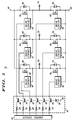
- high voltage bridge interface circuit 10 including control circuit 12 having six output terminals coupled through resistors 14, 16, 18, 20, 22, and 24, respectively, to the emitters of PNP transistors 26, 28, 30, 32, 34 and 36.
- the bases of PNP transistors 26-36 are commonly coupled to the cathode of zener diode 38, while the anode is coupled to power supply conductor 40 typically operating at ground potential.
- Resistors 14-24, PNP transistors 26-36 and zener diode 38 comprise high voltage isolation circuit 42.
- the collectors of PNP transistors 26-36 are coupled to the inputs of turn-on/turn-off drive circuits 44, 46, 48, 50, 52, and 54, while the first outputs of drive circuits 44-54 are coupled to the gate terminals of transistors 56, 58, 60, 62, 64, and 66, respectively.
- Transistors 56-66 are typically discrete power MOSFET devices.
- the source terminals of transistors 56, 58, and 60 are coupled to the second outputs of drive circuits 44, 46, and 48, respectively, and to power supply conductor 68 typically operating at -300 volts DC.
- the drain terminals of transistors 62, 64, and 66 are coupled to power supply conductor 69, while the source terminals of the same are coupled to the second outputs of drive circuits 50, 52, and 54 and to the drain terminals of transistors 56, 58, and 60, respectively.
- Outputs 70, 72, and 74 are coupled to the stator windings of an AC or brushless DC motor at the drain terminals of transistors 56, 58, and 60, respectively.
- diodes 76, 78, 80, 82, 84, and 86 are coupled between the drain and source terminals of transistors 56-66 for providing conventional reverse bias protection.
- drive circuit 44 including diode 90 having anode and cathode terminals coupled to the input and first output of drive circuit 44, respectively.
- the collector of transistor 92 is coupled to the anode of diode 90, while the emitter is coupled to the second output of drive circuit 44.
- the collector and base of transistor 92 are coupled to the base and collector of transistor 94, respectively, and the emitter of the latter is coupled to the cathode of diode 90.
- Resistor 96 is coupled between the base and emitter of transistor 92, and resistor 98 is coupled between the collector and emitter of transistor 92.
- zener diode 100 is coupled between the first and second outputs of drive circuit 44 for supplying a positive clamp at the first output with respect to the second output thereof.
- control circuit 12 develops output voltage pulses each having a predetermined phase relationship, such as disclosed in the literature for Motorola part number MC33034.
- the output terminals of control circuit 12 are commonly known as phase-A, phase-B and phase-C; bottom-side and top-side output terminals.
- the phase-A bottom-side and phase-A top-side output terminals may for example be coupled to resistors 14 and 20, while the phase-B bottom-side and phase-B top-side output terminals are coupled to resistors 16 and 22, respectively.
- the bottom-side and top-side output pulses of a particular phase have approximate 30 degrees of phase shift therebetween, e.g., there is 30 degree phase differential between phase-A bottom-side and phase-A top-side output pulses. Furthermore, there is 120 degree phase relationship between the phase-A, phase-B and phase-C common output pulses.
- a metal mask option wherein the top-side output pulses are inverted and the bottom-side and top-side output terminals are swapped relative to the standard part usage.
- the standard part phase-A top-side output is inverted and coupled to the conduction path leading to the phase-A bottom-side transistor, while the standard part phase-A bottom-side output terminal is coupled to the conduction path leading to phase-A top-side transistor.
- the top-side transistors are pulse width modulated via control circuit 12 to control the rotational speed within the on-period, while the bottom-side transistors are commutated to steer the stator currents.
- a common base operating frequency for control circuit 12 is 25 KHz.
- the potential developed at the gate of transistor 56 increases and clamps to zener voltage, approximately 10.4 volts, rendering it conductive and pulling the voltage at output 70 to one saturation potential above power supply conductor 68 thereby sinking current from the phase-A stator winding.
- the excess current not required by transistor 56 flows through zener diode 100 into the source terminal of transistor 56.
- the forward biased state of diode 90 reverse biases the base-emitter junction of transistor 94 turn it off as well as transistor 92.
- the output pulse of the phase-A bottom-side output terminal drops low, the output pulse of the phase-C bottom-side output terminal transitions high turning on transistor 60 via drive circuit 48 in the same manner described for drive circuit 44 thereby commencing the phase-C sub-cycle.
- the output pulse of the phase-A top-side output terminal goes high turning on transistor 62 through drive circuit 50.
- the drain-source conduction path through transistor 62 supplies current from power supply conductor 69 through output 70 into the phase-A stator windings.
- the phase-B and phase-C sub-cycles source and sink stator current through outputs 72 and 74.
- resistors 14-24 should be selected such that at least two milliamps (mA) of current flows into the associated drive circuits; one mA of current to maintain the conduction through zener diode 100 and one mA of current flowing through resistor 98.
- Drive circuits 46, 48, 50, 52 and 54 comprise the same components and operate as described for drive circuit 44.
- High voltage isolation circuit 42 provides unilateral isolation between control circuit 12 and high voltage power supply conductors 68 and 69.
- PNP transistors 26-36 are conducting the potentials developed at the collectors thereof can reach -300 VDC; however, the potentials at the emitters never exceed the operating potential of control circuit 12, thus, the high voltage between power supply conductors 68 and 69 is maintained across the collector-emitter junctions of PNP transistors 26-36 and never reaches control circuit 12.
- the gate-source potentials of transistors 56-66 are established via zener diode 100 referenced to the source terminal thereof and enabled through the current flowing through PNP transistors 26-36 into drive circuits 44-54, respectively, thereby eliminating the need for an extraneous charge pump circuit. Furthermore, since the top-side transistors are the ones pulse width modulated, the source terminals of the bottom-side transistors are essentially at AC ground thereby providing a greatly reduced voltage swing at the gate terminals of the latter which improves the noise immunity for the power MOSFETs.
- control circuit 12 is enclosed in one IC while high voltage isolation circuit 42 including resistors 14-24, PNP transistors 26-36 and zener diode 38 comprise another IC, hence, the control IC (12) is physically separated from the high voltage interface IC (42).
- Drive circuits 44-54 may also be integrated into one IC, or separated into six individual ICs.
- power MOSFETs 56-66 are discrete devices.
- the present invention has partitioned the motor control components by providing the high voltage interface within one IC thereby permitting integration of the discrete components of the power MOSFET drive circuits and simplifying the overall system integration.
Landscapes
- Engineering & Computer Science (AREA)
- Power Engineering (AREA)
- Control Of Motors That Do Not Use Commutators (AREA)
- Control Of Direct Current Motors (AREA)
- Control Of Ac Motors In General (AREA)
Claims (5)
- Eine Motorsteuerungsschaltung (10) zum Aufnehmen und Speisen von Strom über einen Ausgang (70), die ein erstes Mittel (12) enthält, welches eine Vielzahl von Ausgängen zum Bereitstellen einer Vielzahl von eine vorherbestimmte Beziehung zueinander aufweisenden Steuersignalen besitzt, und die einen ersten (62) und einen zweiten (56) Leistungstransistor besitzt, von denen jeder einen Gateanschluß, einen Sourceanschluß und eine Drainanschluß aufweist, wobei der Drainanschluß des ersten Leistungstransistors zu einer ersten Quelle eines Arbeitspotentials (69) verbunden ist, der Sourceanschluß des zweiten Leistungstransistors zu einer zweiten Quelle des Arbeitspotentials (68) verbunden ist, der Sourceanschluß des ersten Leistungstransistors und der Drainanschluß des zweiten Leistungstransistors miteinander und zu dem Ausgang verbunden sind, wobei die Schaltung gekennzeichnet ist durch:• zweite Mittel (42), die auf die Vielzahl der Steuersignale reagieren, zum Ermöglichen und Nicht-Ermöglichen einer Vielzahl von Ausgangssignalen, während dem Bereitstellen einer einseitigen Isolation des ersten Mittels vom sich über dieser ersten und zweiten Quelle des Arbeitspotentials aufbauenden Arbeitspotential, wobei diese zweiten Mittel eine Vielzahl von Transistoren (26-36) enthalten, von denen jeder eine Basis, einen Emitter und einen Kollektor besitzt, wobei diese Basen miteinander zu einer dritten Quelle des Arbeitspotentials (40) verbunden sind, diese Emitter zum Empfangen eines der Vielzahl der Steuersignale verbunden sind, diese Kollektoren des ersten und zweiten Transistor dieser Vielzahl von Transistoren erste und zweite Ausgangssignale dieser Vielzahl von Ausgangssignalen bereitstellen; und• eine erste (50) und eine zweite (44) Treiberschaltung, von denen jede einen Eingang und einen ersten und einen zweiten Ausgang besitzt, wobei diese Eingänge zum Empfangen des ersten bzw. des zweiten Ausgangssignals dieser Vielzahl von Ausgangssignalen dieser zweiten Mittel verbunden sind, diese ersten Ausgänge zu den Gateanschlüssen des ersten bzw. des zweiten Leistungstransistors verbunden sind, diese zweiten Ausgänge zu den Sourceanschlüssen des ersten bzw. zweiten Leistungstransistors verbunden sind.
- Die Schaltung nach Anspruch 1, wobei diese zweiten Mittel weiter enthalten:• eine Vielzahl von Widerständen (14-24), die jeweils zwischen der Vielzahl der Ausgänge des ersten Mittels (12) und diesen Emittern dieser Vielzahl von Transistoren (26-36) geschaltet sind; und• eine Zenerdiode (38), die zwischen diesen Basen dieser Vielzahl von Transistoren (26-36) und dieser dritter Quelle des Arbeitspotentials geschaltet ist, ausgelegt zum Bereitstellen eines positiven Potentials an diesen Basen dieser Vielzahl von Transistoren in Bezug auf diese dritte Quelle des Arbeitspotentials.
- Die Schaltung nach Anspruch 1 oder 2, wobei diese Vielzahl von Transistoren (26-36) PNP-Transistoren sind.
- Die Schaltung nach Anspruch 3, wobei diese erste Treiberschaltung enthält:• erste Diodenmittel (90), die eine zu diesem Eingang dieser ersten Treiberschaltung (44) verbundene Anode besitzen und eine zu diesem ersten Ausgang dieser ersten Treiberschaltung verbundene Kathode besitzen;• einen ersten Transistor (92), der eine Basis, einen Emitter und einen Kollektor besitzt, wobei dieser Kollektor zu dieser Anode dieser ersten Diodenmittel (90) verbunden ist, dieser Emitter zu diesem zweiten Ausgang dieser ersten Treiberschaltung verbunden ist;• einen zweiten Transistor (94), der eine Basis, einen Emitter und einen Kollektor besitzt, wobei diese Basis zu diesem Kollektor dieses ersten Transistors verbunden ist, dieser Emitter zu dieser Kathode dieser ersten Diodenmittel verbunden ist, dieser Kollektor zu dieser Basis dieses ersten Transistors verbunden ist;• einen ersten Widerstand (96), der zwischen dieser Basis und dem Emitter dieses ersten Transistors geschaltet ist;• einen zweiten Widerstand (98), der zwischen diesem Kollektor und dem Emitter dieses ersten Transistors geschaltet ist; und• zweite Diodenmittel (100), die eine zu diesem ersten Ausgang dieser ersten Treiberschaltung verbundene Kathode besitzen und eine zu diesem zweiten Ausgang dieser ersten Treiberschaltung verbundene Anode besitzen.
- Ein Verfahren zur Steuerung einer Motorsteuerungsschaltung (10) in Übereinstimmung mit Anspruch 1, wobei das Verfahren die Schritte umfaßt:• Bereitstellen der Vielzahl von Steuersignalen, die ein vorherbestimmtes Phasenverhältnis zueinander besitzen;• Ermöglichung der Vielzahl von Ausgangssignalen in Antwort auf die Vielzahl von Steuersignalen, während die Isolation für die Vielzahl der Steuersignale von der ersten und der zweiten Quelle des Arbeitspotentials (68, 69) aufrecht erhalten wird; und• liefern eines Ausgangsstromes über den ersten und den zweiten Leistungstransistor (62, 56), die zwischen der ersten und der zweiten Quelle des Arbeitspotentials (68, 69) geschaltet sind, in Antwort auf die Vielzahl der Ausgangssignale.
Applications Claiming Priority (2)
| Application Number | Priority Date | Filing Date | Title |
|---|---|---|---|
| US07/484,946 US4967336A (en) | 1990-02-26 | 1990-02-26 | High voltage bridge interface |
| US484946 | 1990-02-26 |
Publications (3)
| Publication Number | Publication Date |
|---|---|
| EP0444404A2 EP0444404A2 (de) | 1991-09-04 |
| EP0444404A3 EP0444404A3 (en) | 1991-10-23 |
| EP0444404B1 true EP0444404B1 (de) | 1997-10-08 |
Family
ID=23926293
Family Applications (1)
| Application Number | Title | Priority Date | Filing Date |
|---|---|---|---|
| EP91100366A Expired - Lifetime EP0444404B1 (de) | 1990-02-26 | 1991-01-14 | Hochspannungsbrückenschnittstelle für Wechselstrom- und bürstenlose Gleichstrommotor-Steuerung |
Country Status (5)
| Country | Link |
|---|---|
| US (1) | US4967336A (de) |
| EP (1) | EP0444404B1 (de) |
| JP (1) | JPH04229097A (de) |
| KR (1) | KR920000168A (de) |
| DE (1) | DE69127838T2 (de) |
Families Citing this family (9)
| Publication number | Priority date | Publication date | Assignee | Title |
|---|---|---|---|---|
| DE4007566C2 (de) * | 1990-03-09 | 1998-07-16 | Siemens Ag | Leistungsverstärker für die Speisung einer Induktivität mit geschalteten Transistoren |
| US5103148A (en) * | 1990-11-06 | 1992-04-07 | Motorola, Inc. | Low voltage circuit to control high voltage transistor |
| US5517402A (en) * | 1992-06-04 | 1996-05-14 | Sanden Corporation | Inverter circuit with an improved inverter driving circuit |
| IT1266377B1 (it) * | 1993-05-31 | 1996-12-27 | Merloni Antonio Spa | Metodo di alimentazione di motori elettrici a induzione mediante inverter elettronici |
| JP3411437B2 (ja) * | 1996-02-23 | 2003-06-03 | 富士電機株式会社 | 電力用半導体モジュール |
| EP1258980B1 (de) * | 2001-05-17 | 2005-12-07 | STMicroelectronics S.r.l. | Treiberschaltung und Verfahren zur Verhinderung von Überspannungen auf Versorgungsleitungen während des Betriebes eines Gleichstrommotors |
| DE10156939B4 (de) | 2001-11-20 | 2004-06-03 | Robert Bosch Gmbh | Schaltungsanordnung zum Betreiben einer elektrischenMaschine |
| CA3025336A1 (en) * | 2010-09-30 | 2012-03-30 | Philips Lighting Holding B.V. | Apparatus and methods for supplying power |
| KR102167778B1 (ko) * | 2013-12-04 | 2020-10-20 | 엘지이노텍 주식회사 | 손떨림 보정 액추에이터 고전류 제어 시스템 |
Family Cites Families (8)
| Publication number | Priority date | Publication date | Assignee | Title |
|---|---|---|---|---|
| JPH0634587B2 (ja) * | 1982-05-06 | 1994-05-02 | 株式会社東芝 | 電圧形インバータ装置 |
| US4481434A (en) * | 1982-06-21 | 1984-11-06 | Eaton Corporation | Self regenerative fast gate turn-off FET |
| JPS59123478A (ja) * | 1982-12-28 | 1984-07-17 | Toshiba Corp | 電圧形インバ−タの制御装置 |
| JPH0634594B2 (ja) * | 1983-10-07 | 1994-05-02 | 株式会社東芝 | 電圧形インバ−タ |
| JPS6373898A (ja) * | 1986-09-12 | 1988-04-04 | Matsushita Electric Ind Co Ltd | インバ−タ装置 |
| KR900008393B1 (ko) * | 1986-10-02 | 1990-11-17 | 미츠비시 덴키 가부시키가이샤 | 인버터장치의 과전류보호회로 |
| JP2578159B2 (ja) * | 1988-04-18 | 1997-02-05 | 日本オーチス・エレベータ株式会社 | Pwmインバータ |
| US4875148A (en) * | 1988-12-16 | 1989-10-17 | Sundstrand Corporation | Control for producing a low magnitude voltage at the output of a PWM inverter |
-
1990
- 1990-02-26 US US07/484,946 patent/US4967336A/en not_active Expired - Lifetime
-
1991
- 1991-01-14 EP EP91100366A patent/EP0444404B1/de not_active Expired - Lifetime
- 1991-01-14 DE DE69127838T patent/DE69127838T2/de not_active Expired - Fee Related
- 1991-02-20 KR KR1019910002698A patent/KR920000168A/ko not_active Withdrawn
- 1991-02-26 JP JP3114207A patent/JPH04229097A/ja active Pending
Also Published As
| Publication number | Publication date |
|---|---|
| DE69127838T2 (de) | 1998-03-26 |
| KR920000168A (ko) | 1992-01-10 |
| DE69127838D1 (de) | 1997-11-13 |
| US4967336A (en) | 1990-10-30 |
| JPH04229097A (ja) | 1992-08-18 |
| EP0444404A2 (de) | 1991-09-04 |
| EP0444404A3 (en) | 1991-10-23 |
Similar Documents
| Publication | Publication Date | Title |
|---|---|---|
| EP0365618B1 (de) | Elektronische steuerschaltungen, elektronisch geschaltete motorsysteme und verfahren | |
| US4472666A (en) | Brushless DC motor | |
| EP0814564A1 (de) | Elektronischer Schaltkreis mit reduzierten Schalttransienten | |
| EP0148855B1 (de) | Paralleler "mosfet"-kraftstromschaltungskreis | |
| US4740734A (en) | Control apparatus for brushless dc motors | |
| EP0444404B1 (de) | Hochspannungsbrückenschnittstelle für Wechselstrom- und bürstenlose Gleichstrommotor-Steuerung | |
| US5764019A (en) | Control circuit and system for a switched reluctance machine and method of operating | |
| US5668450A (en) | Half-wave, brushless, four-phase DC motor with bifilar windings | |
| GB1560413A (en) | Dynamoelectric machines | |
| JPS6131424B2 (de) | ||
| US5764007A (en) | Micro-processor based motor control integrated circuit including a boost regulated DC-to-DC converter | |
| US5514939A (en) | Circuitry for switching the body nodes of driver transistors in drive circuitry for brushless DC motors | |
| CA2009581A1 (en) | Current controlled full wave transistor bridge inverter for a multiple phase ac machine | |
| US3688172A (en) | Commutating device for brushless motor including magnetic diodes | |
| US4242624A (en) | Direct current stepper motor with a permanent magnet rotor and electronic commutation device | |
| JPS644439B2 (de) | ||
| US5541487A (en) | Driving circuit for stepping motor | |
| US3541408A (en) | Speed control circuit for brushless dc motor | |
| US5572096A (en) | Method and circuit for clamping the recirculation current in stator windings | |
| US3873898A (en) | Physical condition responsive transducer system, particularly magnetic field transducer system especially for use in or combination with brushless D-C motors | |
| US6548983B2 (en) | PWM-pulse control system | |
| US4520279A (en) | Series transistor chopper | |
| Jahns | Designing intelligent muscle into industrial motion control | |
| US4458191A (en) | Step motor drive circuit | |
| US5886487A (en) | DC motor driver having output FETS that conduct to rectify output overvoltage and undervoltage transients |
Legal Events
| Date | Code | Title | Description |
|---|---|---|---|
| PUAI | Public reference made under article 153(3) epc to a published international application that has entered the european phase |
Free format text: ORIGINAL CODE: 0009012 |
|
| PUAL | Search report despatched |
Free format text: ORIGINAL CODE: 0009013 |
|
| AK | Designated contracting states |
Kind code of ref document: A2 Designated state(s): DE FR GB IT |
|
| AK | Designated contracting states |
Kind code of ref document: A3 Designated state(s): DE FR GB IT |
|
| 17P | Request for examination filed |
Effective date: 19920201 |
|
| 17Q | First examination report despatched |
Effective date: 19931202 |
|
| GRAG | Despatch of communication of intention to grant |
Free format text: ORIGINAL CODE: EPIDOS AGRA |
|
| GRAH | Despatch of communication of intention to grant a patent |
Free format text: ORIGINAL CODE: EPIDOS IGRA |
|
| GRAH | Despatch of communication of intention to grant a patent |
Free format text: ORIGINAL CODE: EPIDOS IGRA |
|
| GRAA | (expected) grant |
Free format text: ORIGINAL CODE: 0009210 |
|
| AK | Designated contracting states |
Kind code of ref document: B1 Designated state(s): DE FR GB IT |
|
| REF | Corresponds to: |
Ref document number: 69127838 Country of ref document: DE Date of ref document: 19971113 |
|
| ITF | It: translation for a ep patent filed | ||
| PGFP | Annual fee paid to national office [announced via postgrant information from national office to epo] |
Ref country code: GB Payment date: 19971229 Year of fee payment: 8 |
|
| PGFP | Annual fee paid to national office [announced via postgrant information from national office to epo] |
Ref country code: FR Payment date: 19980116 Year of fee payment: 8 |
|
| PGFP | Annual fee paid to national office [announced via postgrant information from national office to epo] |
Ref country code: DE Payment date: 19980120 Year of fee payment: 8 |
|
| ET | Fr: translation filed | ||
| PLBE | No opposition filed within time limit |
Free format text: ORIGINAL CODE: 0009261 |
|
| STAA | Information on the status of an ep patent application or granted ep patent |
Free format text: STATUS: NO OPPOSITION FILED WITHIN TIME LIMIT |
|
| 26N | No opposition filed | ||
| PG25 | Lapsed in a contracting state [announced via postgrant information from national office to epo] |
Ref country code: GB Free format text: LAPSE BECAUSE OF NON-PAYMENT OF DUE FEES Effective date: 19990114 |
|
| GBPC | Gb: european patent ceased through non-payment of renewal fee |
Effective date: 19990114 |
|
| PG25 | Lapsed in a contracting state [announced via postgrant information from national office to epo] |
Ref country code: FR Free format text: LAPSE BECAUSE OF NON-PAYMENT OF DUE FEES Effective date: 19990930 |
|
| PG25 | Lapsed in a contracting state [announced via postgrant information from national office to epo] |
Ref country code: DE Free format text: LAPSE BECAUSE OF NON-PAYMENT OF DUE FEES Effective date: 19991103 |
|
| REG | Reference to a national code |
Ref country code: FR Ref legal event code: ST |
|
| PG25 | Lapsed in a contracting state [announced via postgrant information from national office to epo] |
Ref country code: IT Free format text: LAPSE BECAUSE OF NON-PAYMENT OF DUE FEES Effective date: 20050114 |