EP0443852A1 - Lateraler Heterogrenzflächen-Bipolartransistor - Google Patents
Lateraler Heterogrenzflächen-Bipolartransistor Download PDFInfo
- Publication number
- EP0443852A1 EP0443852A1 EP91301383A EP91301383A EP0443852A1 EP 0443852 A1 EP0443852 A1 EP 0443852A1 EP 91301383 A EP91301383 A EP 91301383A EP 91301383 A EP91301383 A EP 91301383A EP 0443852 A1 EP0443852 A1 EP 0443852A1
- Authority
- EP
- European Patent Office
- Prior art keywords
- area
- emitter
- base
- semiconductor device
- barrier
- Prior art date
- Legal status (The legal status is an assumption and is not a legal conclusion. Google has not performed a legal analysis and makes no representation as to the accuracy of the status listed.)
- Granted
Links
- 239000004065 semiconductor Substances 0.000 claims abstract description 56
- 238000009792 diffusion process Methods 0.000 claims description 75
- 239000012535 impurity Substances 0.000 claims description 66
- 239000000969 carrier Substances 0.000 claims description 41
- 230000004888 barrier function Effects 0.000 claims description 40
- 239000010408 film Substances 0.000 claims description 19
- 239000000463 material Substances 0.000 claims description 9
- ZOXJGFHDIHLPTG-UHFFFAOYSA-N Boron Chemical group [B] ZOXJGFHDIHLPTG-UHFFFAOYSA-N 0.000 claims description 8
- 229910052796 boron Inorganic materials 0.000 claims description 8
- 239000010409 thin film Substances 0.000 claims description 5
- 239000000758 substrate Substances 0.000 description 37
- 230000006798 recombination Effects 0.000 description 30
- 238000005215 recombination Methods 0.000 description 30
- 239000013078 crystal Substances 0.000 description 27
- 230000003321 amplification Effects 0.000 description 20
- 238000003199 nucleic acid amplification method Methods 0.000 description 20
- 229910006990 Si1-xGex Inorganic materials 0.000 description 17
- 229910007020 Si1−xGex Inorganic materials 0.000 description 17
- 229910008310 Si—Ge Inorganic materials 0.000 description 15
- 238000009826 distribution Methods 0.000 description 14
- 239000002184 metal Substances 0.000 description 12
- 229910052751 metal Inorganic materials 0.000 description 12
- 238000013459 approach Methods 0.000 description 9
- 238000010438 heat treatment Methods 0.000 description 8
- 238000005036 potential barrier Methods 0.000 description 8
- 230000000694 effects Effects 0.000 description 7
- 150000002500 ions Chemical class 0.000 description 7
- 229910052710 silicon Inorganic materials 0.000 description 7
- 229910045601 alloy Inorganic materials 0.000 description 6
- 239000000956 alloy Substances 0.000 description 6
- 229910021421 monocrystalline silicon Inorganic materials 0.000 description 6
- 229910021420 polycrystalline silicon Inorganic materials 0.000 description 6
- 229910018125 Al-Si Inorganic materials 0.000 description 5
- 229910018520 Al—Si Inorganic materials 0.000 description 5
- 238000005468 ion implantation Methods 0.000 description 5
- 239000010703 silicon Substances 0.000 description 5
- XUIMIQQOPSSXEZ-UHFFFAOYSA-N Silicon Chemical compound [Si] XUIMIQQOPSSXEZ-UHFFFAOYSA-N 0.000 description 4
- 238000004519 manufacturing process Methods 0.000 description 4
- 230000003647 oxidation Effects 0.000 description 4
- 238000007254 oxidation reaction Methods 0.000 description 4
- 229910001218 Gallium arsenide Inorganic materials 0.000 description 3
- OAICVXFJPJFONN-UHFFFAOYSA-N Phosphorus Chemical compound [P] OAICVXFJPJFONN-UHFFFAOYSA-N 0.000 description 3
- 229910052787 antimony Inorganic materials 0.000 description 3
- 229910052785 arsenic Inorganic materials 0.000 description 3
- 230000015572 biosynthetic process Effects 0.000 description 3
- 230000008859 change Effects 0.000 description 3
- 238000002513 implantation Methods 0.000 description 3
- 238000009413 insulation Methods 0.000 description 3
- 238000000034 method Methods 0.000 description 3
- 238000002161 passivation Methods 0.000 description 3
- 229910052698 phosphorus Inorganic materials 0.000 description 3
- 238000000926 separation method Methods 0.000 description 3
- 238000004544 sputter deposition Methods 0.000 description 3
- IJGRMHOSHXDMSA-UHFFFAOYSA-N Atomic nitrogen Chemical compound N#N IJGRMHOSHXDMSA-UHFFFAOYSA-N 0.000 description 2
- 230000015556 catabolic process Effects 0.000 description 2
- 230000003503 early effect Effects 0.000 description 2
- 230000007480 spreading Effects 0.000 description 2
- 238000003892 spreading Methods 0.000 description 2
- 230000008901 benefit Effects 0.000 description 1
- 150000001875 compounds Chemical class 0.000 description 1
- 239000012141 concentrate Substances 0.000 description 1
- 230000003247 decreasing effect Effects 0.000 description 1
- 238000005516 engineering process Methods 0.000 description 1
- 238000000407 epitaxy Methods 0.000 description 1
- 238000002347 injection Methods 0.000 description 1
- 239000007924 injection Substances 0.000 description 1
- 230000010354 integration Effects 0.000 description 1
- 239000007788 liquid Substances 0.000 description 1
- 229910021424 microcrystalline silicon Inorganic materials 0.000 description 1
- 229910052757 nitrogen Inorganic materials 0.000 description 1
- 238000009751 slip forming Methods 0.000 description 1
Images


Classifications
-
- H—ELECTRICITY
- H01—ELECTRIC ELEMENTS
- H01L—SEMICONDUCTOR DEVICES NOT COVERED BY CLASS H10
- H01L29/00—Semiconductor devices adapted for rectifying, amplifying, oscillating or switching, or capacitors or resistors with at least one potential-jump barrier or surface barrier, e.g. PN junction depletion layer or carrier concentration layer; Details of semiconductor bodies or of electrodes thereof ; Multistep manufacturing processes therefor
- H01L29/02—Semiconductor bodies ; Multistep manufacturing processes therefor
- H01L29/06—Semiconductor bodies ; Multistep manufacturing processes therefor characterised by their shape; characterised by the shapes, relative sizes, or dispositions of the semiconductor regions ; characterised by the concentration or distribution of impurities within semiconductor regions
- H01L29/10—Semiconductor bodies ; Multistep manufacturing processes therefor characterised by their shape; characterised by the shapes, relative sizes, or dispositions of the semiconductor regions ; characterised by the concentration or distribution of impurities within semiconductor regions with semiconductor regions connected to an electrode not carrying current to be rectified, amplified or switched and such electrode being part of a semiconductor device which comprises three or more electrodes
- H01L29/1004—Base region of bipolar transistors
- H01L29/1008—Base region of bipolar transistors of lateral transistors
-
- H—ELECTRICITY
- H01—ELECTRIC ELEMENTS
- H01L—SEMICONDUCTOR DEVICES NOT COVERED BY CLASS H10
- H01L29/00—Semiconductor devices adapted for rectifying, amplifying, oscillating or switching, or capacitors or resistors with at least one potential-jump barrier or surface barrier, e.g. PN junction depletion layer or carrier concentration layer; Details of semiconductor bodies or of electrodes thereof ; Multistep manufacturing processes therefor
- H01L29/02—Semiconductor bodies ; Multistep manufacturing processes therefor
- H01L29/06—Semiconductor bodies ; Multistep manufacturing processes therefor characterised by their shape; characterised by the shapes, relative sizes, or dispositions of the semiconductor regions ; characterised by the concentration or distribution of impurities within semiconductor regions
- H01L29/08—Semiconductor bodies ; Multistep manufacturing processes therefor characterised by their shape; characterised by the shapes, relative sizes, or dispositions of the semiconductor regions ; characterised by the concentration or distribution of impurities within semiconductor regions with semiconductor regions connected to an electrode carrying current to be rectified, amplified or switched and such electrode being part of a semiconductor device which comprises three or more electrodes
- H01L29/0895—Tunnel injectors
-
- H—ELECTRICITY
- H01—ELECTRIC ELEMENTS
- H01L—SEMICONDUCTOR DEVICES NOT COVERED BY CLASS H10
- H01L29/00—Semiconductor devices adapted for rectifying, amplifying, oscillating or switching, or capacitors or resistors with at least one potential-jump barrier or surface barrier, e.g. PN junction depletion layer or carrier concentration layer; Details of semiconductor bodies or of electrodes thereof ; Multistep manufacturing processes therefor
- H01L29/02—Semiconductor bodies ; Multistep manufacturing processes therefor
- H01L29/12—Semiconductor bodies ; Multistep manufacturing processes therefor characterised by the materials of which they are formed
- H01L29/16—Semiconductor bodies ; Multistep manufacturing processes therefor characterised by the materials of which they are formed including, apart from doping materials or other impurities, only elements of Group IV of the Periodic System
- H01L29/161—Semiconductor bodies ; Multistep manufacturing processes therefor characterised by the materials of which they are formed including, apart from doping materials or other impurities, only elements of Group IV of the Periodic System including two or more of the elements provided for in group H01L29/16, e.g. alloys
- H01L29/165—Semiconductor bodies ; Multistep manufacturing processes therefor characterised by the materials of which they are formed including, apart from doping materials or other impurities, only elements of Group IV of the Periodic System including two or more of the elements provided for in group H01L29/16, e.g. alloys in different semiconductor regions, e.g. heterojunctions
-
- H—ELECTRICITY
- H01—ELECTRIC ELEMENTS
- H01L—SEMICONDUCTOR DEVICES NOT COVERED BY CLASS H10
- H01L29/00—Semiconductor devices adapted for rectifying, amplifying, oscillating or switching, or capacitors or resistors with at least one potential-jump barrier or surface barrier, e.g. PN junction depletion layer or carrier concentration layer; Details of semiconductor bodies or of electrodes thereof ; Multistep manufacturing processes therefor
- H01L29/66—Types of semiconductor device ; Multistep manufacturing processes therefor
- H01L29/68—Types of semiconductor device ; Multistep manufacturing processes therefor controllable by only the electric current supplied, or only the electric potential applied, to an electrode which does not carry the current to be rectified, amplified or switched
- H01L29/70—Bipolar devices
- H01L29/72—Transistor-type devices, i.e. able to continuously respond to applied control signals
- H01L29/73—Bipolar junction transistors
- H01L29/735—Lateral transistors
-
- H—ELECTRICITY
- H01—ELECTRIC ELEMENTS
- H01L—SEMICONDUCTOR DEVICES NOT COVERED BY CLASS H10
- H01L29/00—Semiconductor devices adapted for rectifying, amplifying, oscillating or switching, or capacitors or resistors with at least one potential-jump barrier or surface barrier, e.g. PN junction depletion layer or carrier concentration layer; Details of semiconductor bodies or of electrodes thereof ; Multistep manufacturing processes therefor
- H01L29/66—Types of semiconductor device ; Multistep manufacturing processes therefor
- H01L29/68—Types of semiconductor device ; Multistep manufacturing processes therefor controllable by only the electric current supplied, or only the electric potential applied, to an electrode which does not carry the current to be rectified, amplified or switched
- H01L29/70—Bipolar devices
- H01L29/72—Transistor-type devices, i.e. able to continuously respond to applied control signals
- H01L29/73—Bipolar junction transistors
- H01L29/737—Hetero-junction transistors
Definitions
- the depth of the interface constituting said barrier is made shallower than the depth of said emitter and collector areas to concentrate the emitter current in the vicinity of the surface of the substrate.
- Such current concentration close to the surface of the substrate allows to make the active area of the device thinner, thereby responding to the requirements of higher level of integration and finer geometry.
- a silicon substrate 1 is composed, in the present embodiment, of a p-substrate doped with a p-type impurity capable of controlling the conductive type in the p-type, such as boron (B).
- a p-type impurity capable of controlling the conductive type in the p-type such as boron (B).
- the potential distribution along the line B-B' in Fig. 1 is similar to that in the usual bipolar transistor, and the collector current I c can be easily calculated as it is determined by the concentration N B of the base area B R and the base width W s .
- the emitter area and the collector area mutually face only in a very small area, while they are extended quite widely along the surface of the substrate.
- the collector current flows only through the mutually facing area of the emitter and the collector.
- the base current is principally governed by a current generated by the recombination of the positive holes, injected from the emitter area E R into the base area B R in the direction of depth of the substrate, with the electrons constituting the majority carriers, and a diffusion current contributed by the electrons injected from the base area into the emitter area, and becomes large because of a wide area involved.
- the collector current I e between the mutually opposed emitter and collector can be substantially determined by the following equation.
- the life ⁇ p of the minority carriers is represented by the following equation when the impurity concentration exceeds 1017 [cm-3 ]:
- the diffusion length Lp of positive holes is generally represented by:
- the semiconductor device of the first embodiment was prepared through the above-explained procedure.
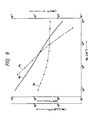
- Fig. 4 shows the change in the band gap of the mixed crystal Si 1-x Ge x , wherein the abscissa indicates the mixed crystal ratio of Ge (X ⁇ 100%) whereas the ordinate indicates decrease -AE in the band gap in comparison with the Si single crystal.
- a curve H o indicates a distortion-free state whereas a curve H u indicates a distorted state, which is selected in a semiconductor device.
- the present invention utilizes a phenomenon that the p-n injection efficiency varies in the p-n junction between the n-area 4 and the p -area 5 because of a smaller band gap in comparison with the p-n junction between the p -area 5 and the n-area 3.
- the present 2nd embodiment is different from the 1st embodiment in that the hole recombination current 1 82 is given by multiplying the equation (3) with a factor exp(- ⁇ E/kT), and that the diffusion current I B3 is also given by multiplying the equation (4) with a factor exp(-AE/kT).
- An increase in the current amplification factor h FE is attained by these features.
- the area 4 may be made shallower than the areas 5, 5'.
- the n-area 4 consisting of mixed crystal Si 1-x Ge x is not formed by ion implantation but by epitaxial growth, and p -areas 5, 5' constituting the emitter and collector areas are subsequently formed therein.
- the contact of the base area is also formed by mixed crystal, but this is not critical.
- the area 4 may be formed shallower than the areas 5, 5' as long as the collector current can be confined in the area 4 by the difference in the band gap.
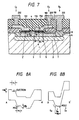
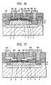
- Fig. 7 illustrates a 4th embodiment of the present invention.
- a silicon substrate 1 is composed, in the present embodiment, of a p-substrate doped with a p-type impurity capable of controlling the conductive type in the p-type, such as boron (B).
- a p-type impurity capable of controlling the conductive type in the p-type such as boron (B).
- An n-area 4 constituting a feature of the present invention is composed of a mixed crystal Si 1-x Ge x with a narrow forbidden band, and constitutes the base area B R .
- the base current is principally governed by a current generated by the recombination of the positive holes, injected from the emitter area E R into the base area B R in the direction of depth of the substrate, with the electrons constituting the majority carriers, and a diffusion current contributed by the electrons injected from the base area into the emitter area, and becomes large because of a wide area involved.
- the magnitude of the emitter area opposed to the collector area in a horizontal bipolar transistor can be approximately represented by ⁇ E ⁇ L wherein Y E and L are respectively the depth and length of the emitter.
- q is elementary change [C]
- Dp is diffusion coefficient [cm 2 /s] of positive holes
- Lp diffusion length [cm] of positive holes
- n i true carrier density [cm- 3 ]
- V BE is emitter-base voltage
- W B is base width [cm]
- N B is base impurity concentration [cm- 3 ]
- X E is emitter depth
- L is emitter length
- k Boltzman constant [J/K]
- T absolute temperature [° K].
- the probability of passing through said barrier is represented by exp(- ⁇ B /kT), as already explained before.
- the life T p of the minority carriers is represented by the following equation when the impurity concentration exceeds 1017 [cm-3 ]:
- said diffusion current I B3 is considerably large, because a metal electrode is formed directly above the emitter area 5.
- the diffusion length L n is generally represented by:
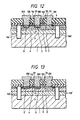
- Fig. 11 illustrates a 6th embodiment.
- the element separating area 100 has a groove structure and mutually separates the n-areas 2, 3, 4 and 50. 120 indicates an oxide film.
- An n -area 6 connects said embedded area 2 with a metal base electrode 201, in order to reduce the base resistance of the horizontal bipolar transistor.
- n-area 7 and a p-area 8 constitute channel stops.
- Polycrystalline semiconductive layers 930, 931 are composed of polycrystalline silicon doped with boron ( B ) at a high concentration (for example 1018 - 1020 [cm -3 ]).
- a barrier ⁇ B consisting of a heterogeneous interface between the emitter area and a semiconductor layer is formed at a depth ⁇ B from said emitter area, and, above the emitter area, there are formed a thin tunnel film and a polycrystalline silicon layer 930 of a wider forbidden band than in said emitter area, in order to prevent the diffusion of the electrons injected into said emitter area.
- the collector current I C between the mutually opposed emitter and collector can be substantially determined by the following equation.
- the magnitude of the emitter area opposed to the collector area in a horizontal bipolar transistor can be approximately represented by ⁇ E ⁇ L wherein X E and L are respectively the depth and length of the emitter.
- q is elementary charge [C]
- Dp is diffusion coefficient [cm 2 /s] of positive holes
- Lp diffusion length [cm] of positive holes
- n is true carrier density [cm- 3 ]
- V BE is emitterbase voltage
- W B is base width [cm]
- N B is base impurity concentration [cm -3 ]
- T E is emitter depth
- L is emitter length
- K is Boltzman constant [J/K]
- T absolute temperature [°K].
- the base current I B is principally composed of three components shown in the following equations (2) - (4).
- the life ⁇ p of the minority carriers is represented by the following equation when the impurity concentration exceeds 1017 [cm-3 ]:
- the diffusion length Lp of positive holes is generally represented by:
- the impurity concentration of the base area becomes same as that of the collector area of said vertical bipolar transistor npn type and is as low as 10 14 - 5 x 10 17 [cm- 3 ], so that the relation can be easily obtained.
- a condition of about is desirable.
- the base current I B is predominantly governed by the recombination current I B1 and the diffusion current I B3 , whereas in the conventional horizontal bipolar transistor, it is predominantly governed by the diffusion current I B3 .
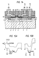
- a polycrystalline layer 930 of a wider forbidden band than in said emitter area as shown in Fig. 15A, thereby preventing the diffusion of electrons.
- said diffusion current I S3 is considerably large, because a metal electrode is formed directly above the emitter area 5.
- the diffusion current I B3 is proportional to W E /L n 2 as will be understood from the equation (4), but, in the conventional horizontal bipolar transistor, it is proportional to 1/WE.
- I S3 in the horizontal bipolar transistor of the present invention is smaller, by a ratio of W E 2 /L n 2 , than that in the conventional horizontal bipolar transistor.
- the life ⁇ n of the minority carriers is represented by the following equation for an impurity concentration equal to or larger than 10 17 [cm -3 ]:
- the diffusion length L n is generally represented by:
- Si 1-x Ge x constituting said n-area 4 shows a small carrier mobility due to the alloy effect, but, under a high impurity concentration for example equal to higher than 10 18 [cm- 3 ], it behaves like Si because the carrier effect by the impurities becomes predominant.
- the base current approaches to the value of the recombination current I B1
- the current amplification factor h FE approaches to that of the vertical heterogeneous bipolar transistor.
- the theoretical current amplification factor in such state if a condition W B ⁇ Lp is satisfied, can be represented by:
- the semiconductor device shown in Fig. 14 was prepared through the above-explained procedure.
- the contact area of the base area may naturally be composed of Si-Ge mixed crystal in order to reduce the contact resistance.
- the present invention is naturally applicable to a horizontal bipolar transistor of npn type.
- a heterogeneous junction of mixed crystals of other materials For example, Si and Si-Ge may be respectively replaced for example by GaAs and GaAIAs, or Inp and InGaPAs.
- the p-n junction between said n-area 4 and the p -area 5 is formed in Si-Ge, while other p-n junctions are formed in Si.
- the band gap in Si-Ge is smaller than in Si as shown in Fig. 4
- the present invention can provide a semiconductor device including a horizontal bipolar transistor which has a high emitter-collector breakdown voltage, is capable of suppressing so-called early effect, and has a low base current, thereby capable of increasing the current amplification factor h FE .
- the present invention can provide a semiconductor device excellent in resistance to ambient conditions.
- the value x in Si 1-x Ge x is preferably at least equal to 0.03, because AE needs to be at least to kT.
- kT 25 meV, so that AE functions as a barrier if x is 0.03 or larger.
- x is preferably at least equal to 0.008.
- the upper limit of the value x is preferably 1.
Priority Applications (2)
| Application Number | Priority Date | Filing Date | Title |
|---|---|---|---|
| EP94203107A EP0642171B1 (de) | 1990-02-22 | 1991-02-21 | Lateraler Bipolartransistor |
| EP94203106A EP0642170B1 (de) | 1990-02-22 | 1991-02-21 | Lateraler Bipolartransistor |
Applications Claiming Priority (6)
| Application Number | Priority Date | Filing Date | Title |
|---|---|---|---|
| JP2042067A JP3001600B2 (ja) | 1990-02-22 | 1990-02-22 | 半導体装置 |
| JP42068/90 | 1990-02-22 | ||
| JP42066/90 | 1990-02-22 | ||
| JP42067/90 | 1990-02-22 | ||
| JP2042068A JP3001601B2 (ja) | 1990-02-22 | 1990-02-22 | 半導体装置 |
| JP2042066A JP3001599B2 (ja) | 1990-02-22 | 1990-02-22 | 半導体装置 |
Related Child Applications (3)
| Application Number | Title | Priority Date | Filing Date |
|---|---|---|---|
| EP94203107A Division EP0642171B1 (de) | 1990-02-22 | 1991-02-21 | Lateraler Bipolartransistor |
| EP94203106.3 Division-Into | 1994-10-26 | ||
| EP94203107.1 Division-Into | 1994-10-26 |
Publications (2)
| Publication Number | Publication Date |
|---|---|
| EP0443852A1 true EP0443852A1 (de) | 1991-08-28 |
| EP0443852B1 EP0443852B1 (de) | 1995-05-24 |
Family
ID=27291053
Family Applications (3)
| Application Number | Title | Priority Date | Filing Date |
|---|---|---|---|
| EP94203107A Expired - Lifetime EP0642171B1 (de) | 1990-02-22 | 1991-02-21 | Lateraler Bipolartransistor |
| EP94203106A Expired - Lifetime EP0642170B1 (de) | 1990-02-22 | 1991-02-21 | Lateraler Bipolartransistor |
| EP91301383A Expired - Lifetime EP0443852B1 (de) | 1990-02-22 | 1991-02-21 | Lateraler Heterogrenzflächen-Bipolartransistor |
Family Applications Before (2)
| Application Number | Title | Priority Date | Filing Date |
|---|---|---|---|
| EP94203107A Expired - Lifetime EP0642171B1 (de) | 1990-02-22 | 1991-02-21 | Lateraler Bipolartransistor |
| EP94203106A Expired - Lifetime EP0642170B1 (de) | 1990-02-22 | 1991-02-21 | Lateraler Bipolartransistor |
Country Status (4)
| Country | Link |
|---|---|
| US (1) | US5734183A (de) |
| EP (3) | EP0642171B1 (de) |
| AT (1) | ATE123175T1 (de) |
| DE (3) | DE69109890T2 (de) |
Cited By (4)
| Publication number | Priority date | Publication date | Assignee | Title |
|---|---|---|---|---|
| EP0616370A2 (de) * | 1993-03-16 | 1994-09-21 | Canon Kabushiki Kaisha | Bipolare Halbleiteranordnung die SiGe enthält und Verfahren zur Herstellung |
| EP0657942A2 (de) * | 1993-12-09 | 1995-06-14 | Nortel Networks Corporation | Lateraler Bipolartransistor |
| EP2180517A1 (de) * | 2008-10-24 | 2010-04-28 | Epcos Ag | Bipolarer PNP-Transistor mit seitlichem Kollektor und Herstellungsverfahren |
| EP3116028A3 (de) * | 2013-06-24 | 2017-03-29 | Ideal Power Inc. | Systeme, schaltungen, vorrichtungen und verfahren mit bidirektionalen bipolartransistoren |
Families Citing this family (17)
| Publication number | Priority date | Publication date | Assignee | Title |
|---|---|---|---|---|
| US6034413A (en) * | 1997-02-27 | 2000-03-07 | Texas Instruments Incorporated | High speed biCMOS gate power for power MOSFETs incorporating improved injection immunity |
| EP0881688A1 (de) * | 1997-05-30 | 1998-12-02 | STMicroelectronics S.r.l. | Elektronisches Bauelement vom Typ lateral-bipolar-pnp |
| US5912481A (en) | 1997-09-29 | 1999-06-15 | National Scientific Corp. | Heterojunction bipolar transistor having wide bandgap, low interdiffusion base-emitter junction |
| US6423990B1 (en) | 1997-09-29 | 2002-07-23 | National Scientific Corporation | Vertical heterojunction bipolar transistor |
| US6674103B2 (en) * | 2000-07-31 | 2004-01-06 | The Regents Of The University Of California | HBT with nitrogen-containing current blocking base collector interface and method for current blocking |
| US6362065B1 (en) * | 2001-02-26 | 2002-03-26 | Texas Instruments Incorporated | Blocking of boron diffusion through the emitter-emitter poly interface in PNP HBTs through use of a SiC layer at the top of the emitter epi layer |
| US6459104B1 (en) * | 2001-05-10 | 2002-10-01 | Newport Fab | Method for fabricating lateral PNP heterojunction bipolar transistor and related structure |
| US6670654B2 (en) * | 2002-01-09 | 2003-12-30 | International Business Machines Corporation | Silicon germanium heterojunction bipolar transistor with carbon incorporation |
| US6927140B2 (en) | 2002-08-21 | 2005-08-09 | Intel Corporation | Method for fabricating a bipolar transistor base |
| US7517768B2 (en) * | 2003-03-31 | 2009-04-14 | Intel Corporation | Method for fabricating a heterojunction bipolar transistor |
| CN102386219B (zh) * | 2010-08-31 | 2013-07-24 | 上海华虹Nec电子有限公司 | SiGe HBT工艺中的寄生横向型PNP三极管及制造方法 |
| CN102412280B (zh) * | 2010-09-21 | 2013-09-11 | 上海华虹Nec电子有限公司 | 锗硅hbt工艺中的横向型寄生pnp器件 |
| CN103377918B (zh) * | 2012-04-27 | 2015-10-21 | 中芯国际集成电路制造(上海)有限公司 | Npn异质结双极晶体管及其制造方法 |
| US8558282B1 (en) | 2012-09-08 | 2013-10-15 | International Business Machines Corporation | Germanium lateral bipolar junction transistor |
| CN110556420B (zh) * | 2019-08-23 | 2022-11-04 | 北京工业大学 | 一种掺杂浓度可调的横向SiGe异质结双极晶体管 |
| US11462632B2 (en) | 2020-12-22 | 2022-10-04 | Globalfoundries U.S. Inc. | Lateral bipolar junction transistor device and method of making such a device |
| US11424349B1 (en) | 2021-02-17 | 2022-08-23 | Globalfoundries U.S. Inc. | Extended shallow trench isolation for ultra-low leakage in fin-type lateral bipolar junction transistor devices |
Citations (1)
| Publication number | Priority date | Publication date | Assignee | Title |
|---|---|---|---|---|
| US4672413A (en) * | 1984-04-16 | 1987-06-09 | Trw Inc. | Barrier emitter transistor |
Family Cites Families (2)
| Publication number | Priority date | Publication date | Assignee | Title |
|---|---|---|---|---|
| FR2625612B1 (fr) * | 1987-12-30 | 1990-05-04 | Labo Electronique Physique | Procede de realisation d'un dispositif semiconducteur du type transistor bipolaire a heterojonction |
| US4987468A (en) * | 1988-06-17 | 1991-01-22 | Xerox Corporation | Lateral heterojunction bipolar transistor (LHBT) and suitability thereof as a hetero transverse junction (HTJ) laser |
-
1991
- 1991-02-21 EP EP94203107A patent/EP0642171B1/de not_active Expired - Lifetime
- 1991-02-21 DE DE69109890T patent/DE69109890T2/de not_active Expired - Fee Related
- 1991-02-21 AT AT91301383T patent/ATE123175T1/de not_active IP Right Cessation
- 1991-02-21 DE DE69128364T patent/DE69128364T2/de not_active Expired - Fee Related
- 1991-02-21 DE DE69129376T patent/DE69129376T2/de not_active Expired - Fee Related
- 1991-02-21 EP EP94203106A patent/EP0642170B1/de not_active Expired - Lifetime
- 1991-02-21 EP EP91301383A patent/EP0443852B1/de not_active Expired - Lifetime
-
1995
- 1995-03-29 US US08/412,847 patent/US5734183A/en not_active Expired - Fee Related
Patent Citations (1)
| Publication number | Priority date | Publication date | Assignee | Title |
|---|---|---|---|---|
| US4672413A (en) * | 1984-04-16 | 1987-06-09 | Trw Inc. | Barrier emitter transistor |
Non-Patent Citations (4)
| Title |
|---|
| I.E.E.E. ELECTRON DEVICE LETTERS vol. EDL-7, no. 11, November 1986, pages 632-634, New York, NY, US; M.K. MORAVVEJ-FARSHI et al.: "Improvements in Current Gain and Breakdown Voltage of Silicon MIS Heterojunction Emitter Transistors" * |
| IEEE TRANSACTION ON ELECTRON DEVICES vol. 36, no. 10, October 1989, pages 2156-2164, New York, US; R.L. THORNTON et al.: "Demonstration and Properties of a Planar Heterojunction Bipolar Transistor with Lateral Current Flow" * |
| INTERNATIONAL ELECTRON DEVICES MEETING (IEDM) 11-14 December 1988, pages 889-891, San Francisco, CA, US; D.L. HARAME et al.: "High-Performance Si and SiGe-Base PNP Transistors" * |
| PROCEEDINGS OF THE 1989 BIPOLAR CIRCUITS AND TECHNOLOGY MEETING 18/19 September 1989, pages 186-189, Minneapolis, US; J. WARNOCK et al.: "Boron-Doped Emitters for High-Performance Vertical PNP Transistors" * |
Cited By (8)
| Publication number | Priority date | Publication date | Assignee | Title |
|---|---|---|---|---|
| EP0616370A2 (de) * | 1993-03-16 | 1994-09-21 | Canon Kabushiki Kaisha | Bipolare Halbleiteranordnung die SiGe enthält und Verfahren zur Herstellung |
| EP0616370A3 (de) * | 1993-03-16 | 1995-04-19 | Canon Kk | Bipolare Halbleiteranordnung die SiGe enthält und Verfahren zur Herstellung. |
| US6246104B1 (en) | 1993-03-16 | 2001-06-12 | Canon Kabushiki Kaisha | Semiconductor device and method for manufacturing the same |
| EP0657942A2 (de) * | 1993-12-09 | 1995-06-14 | Nortel Networks Corporation | Lateraler Bipolartransistor |
| EP0657942A3 (de) * | 1993-12-09 | 1995-09-13 | Northern Telecom Ltd | Lateraler Bipolartransistor. |
| EP2180517A1 (de) * | 2008-10-24 | 2010-04-28 | Epcos Ag | Bipolarer PNP-Transistor mit seitlichem Kollektor und Herstellungsverfahren |
| US8410572B2 (en) | 2008-10-24 | 2013-04-02 | Epcos Ag | Bipolar transistor with emitter and/or collector contact structure forming a Schottky contact and method of production |
| EP3116028A3 (de) * | 2013-06-24 | 2017-03-29 | Ideal Power Inc. | Systeme, schaltungen, vorrichtungen und verfahren mit bidirektionalen bipolartransistoren |
Also Published As
| Publication number | Publication date |
|---|---|
| EP0642171A3 (de) | 1995-08-09 |
| EP0642170A3 (de) | 1995-08-09 |
| DE69128364D1 (de) | 1998-01-15 |
| EP0443852B1 (de) | 1995-05-24 |
| ATE123175T1 (de) | 1995-06-15 |
| EP0642171B1 (de) | 1998-05-06 |
| EP0642171A2 (de) | 1995-03-08 |
| DE69109890T2 (de) | 1995-11-02 |
| EP0642170B1 (de) | 1997-12-03 |
| DE69129376D1 (de) | 1998-06-10 |
| DE69129376T2 (de) | 1998-09-24 |
| DE69128364T2 (de) | 1998-04-09 |
| EP0642170A2 (de) | 1995-03-08 |
| US5734183A (en) | 1998-03-31 |
| DE69109890D1 (de) | 1995-06-29 |
Similar Documents
| Publication | Publication Date | Title |
|---|---|---|
| EP0443852A1 (de) | Lateraler Heterogrenzflächen-Bipolartransistor | |
| US5656514A (en) | Method for making heterojunction bipolar transistor with self-aligned retrograde emitter profile | |
| US5289019A (en) | Insulated gate bipolar transistor | |
| JP3462506B2 (ja) | 炭化ケイ素金属絶縁体半導体電界効果トランジスタの単位セルおよびそれを備える炭化ケイ素金属絶縁体半導体電界効果トランジスタ | |
| US5637889A (en) | Composite power transistor structures using semiconductor materials with different bandgaps | |
| CN101271926B (zh) | 高效整流器 | |
| US5679587A (en) | Method of fabricating an integrated circuit with vertical bipolar power transistors and isolated lateral bipolar control transistors | |
| US4466173A (en) | Methods for fabricating vertical channel buried grid field controlled devices including field effect transistors and field controlled thyristors utilizing etch and refill techniques | |
| EP0507454B1 (de) | Halbleiteranordnung mit einem Heteroübergang-Bipolartransistor und Verfahren zu seiner Herstellung | |
| US6011279A (en) | Silicon carbide field controlled bipolar switch | |
| US5272357A (en) | Semiconductor device and electronic device by use of the semiconductor | |
| EP0168325B1 (de) | Ionenimplantation zur Verbreiterung der verbotenen Zone des Emitters in bipolaren Transistoren | |
| US4009484A (en) | Integrated circuit isolation using gold-doped polysilicon | |
| US6570241B2 (en) | Semiconductor device having the effect that the drop in the current gain is kept to the minimum, when the substrate density is amplified and that the variation in the collector current is improved | |
| KR20030047274A (ko) | 초자기정렬 이종접합 바이폴라 소자 및 그 제조방법 | |
| US3614560A (en) | Improved surface barrier transistor | |
| EP0249088B1 (de) | Halbleiteranordnung | |
| US6320211B1 (en) | Semiconductor device and electronic device by use of the semiconductor | |
| US5357135A (en) | Dmost junction breakdown enhancement | |
| JP3001601B2 (ja) | 半導体装置 | |
| JP3001600B2 (ja) | 半導体装置 | |
| EP0431835B1 (de) | Bipolares Halbleiterbauelement | |
| JP3001599B2 (ja) | 半導体装置 | |
| JPH09181091A (ja) | ヘテロ接合バイポーラトランジスタの製造方法 | |
| JPH0496373A (ja) | 半導体装置 |
Legal Events
| Date | Code | Title | Description |
|---|---|---|---|
| PUAI | Public reference made under article 153(3) epc to a published international application that has entered the european phase |
Free format text: ORIGINAL CODE: 0009012 |
|
| AK | Designated contracting states |
Kind code of ref document: A1 Designated state(s): AT BE CH DE DK ES FR GB GR IT LI LU NL SE |
|
| 17P | Request for examination filed |
Effective date: 19920113 |
|
| 17Q | First examination report despatched |
Effective date: 19920731 |
|
| GRAA | (expected) grant |
Free format text: ORIGINAL CODE: 0009210 |
|
| AK | Designated contracting states |
Kind code of ref document: B1 Designated state(s): AT BE CH DE DK ES FR GB GR IT LI LU NL SE |
|
| PG25 | Lapsed in a contracting state [announced via postgrant information from national office to epo] |
Ref country code: LI Effective date: 19950524 Ref country code: GR Free format text: LAPSE BECAUSE OF FAILURE TO SUBMIT A TRANSLATION OF THE DESCRIPTION OR TO PAY THE FEE WITHIN THE PRESCRIBED TIME-LIMIT Effective date: 19950524 Ref country code: ES Free format text: THE PATENT HAS BEEN ANNULLED BY A DECISION OF A NATIONAL AUTHORITY Effective date: 19950524 Ref country code: DK Effective date: 19950524 Ref country code: CH Effective date: 19950524 Ref country code: BE Effective date: 19950524 Ref country code: AT Effective date: 19950524 |
|
| REF | Corresponds to: |
Ref document number: 123175 Country of ref document: AT Date of ref document: 19950615 Kind code of ref document: T |
|
| XX | Miscellaneous (additional remarks) |
Free format text: TEILANMELDUNG 94203107.1 EINGEREICHT AM 21/02/91. |
|
| REF | Corresponds to: |
Ref document number: 69109890 Country of ref document: DE Date of ref document: 19950629 |
|
| ET | Fr: translation filed | ||
| ITF | It: translation for a ep patent filed |
Owner name: SOCIETA' ITALIANA BREVETTI S.P.A. |
|
| PG25 | Lapsed in a contracting state [announced via postgrant information from national office to epo] |
Ref country code: SE Effective date: 19950824 |
|
| REG | Reference to a national code |
Ref country code: CH Ref legal event code: PL |
|
| PG25 | Lapsed in a contracting state [announced via postgrant information from national office to epo] |
Ref country code: LU Free format text: LAPSE BECAUSE OF NON-PAYMENT OF DUE FEES Effective date: 19960229 |
|
| PLBE | No opposition filed within time limit |
Free format text: ORIGINAL CODE: 0009261 |
|
| STAA | Information on the status of an ep patent application or granted ep patent |
Free format text: STATUS: NO OPPOSITION FILED WITHIN TIME LIMIT |
|
| 26N | No opposition filed | ||
| K2C3 | Correction of patent specification (complete document) published |
Effective date: 19950524 |
|
| REG | Reference to a national code |
Ref country code: GB Ref legal event code: IF02 |
|
| PGFP | Annual fee paid to national office [announced via postgrant information from national office to epo] |
Ref country code: GB Payment date: 20050207 Year of fee payment: 15 |
|
| PGFP | Annual fee paid to national office [announced via postgrant information from national office to epo] |
Ref country code: NL Payment date: 20050214 Year of fee payment: 15 |
|
| PGFP | Annual fee paid to national office [announced via postgrant information from national office to epo] |
Ref country code: FR Payment date: 20050216 Year of fee payment: 15 |
|
| PGFP | Annual fee paid to national office [announced via postgrant information from national office to epo] |
Ref country code: DE Payment date: 20050420 Year of fee payment: 15 |
|
| PG25 | Lapsed in a contracting state [announced via postgrant information from national office to epo] |
Ref country code: GB Free format text: LAPSE BECAUSE OF NON-PAYMENT OF DUE FEES Effective date: 20060221 |
|
| PGFP | Annual fee paid to national office [announced via postgrant information from national office to epo] |
Ref country code: IT Payment date: 20060228 Year of fee payment: 16 |
|
| PG25 | Lapsed in a contracting state [announced via postgrant information from national office to epo] |
Ref country code: NL Free format text: LAPSE BECAUSE OF NON-PAYMENT OF DUE FEES Effective date: 20060901 Ref country code: DE Free format text: LAPSE BECAUSE OF NON-PAYMENT OF DUE FEES Effective date: 20060901 |
|
| GBPC | Gb: european patent ceased through non-payment of renewal fee |
Effective date: 20060221 |
|
| NLV4 | Nl: lapsed or anulled due to non-payment of the annual fee |
Effective date: 20060901 |
|
| REG | Reference to a national code |
Ref country code: FR Ref legal event code: ST Effective date: 20061031 |
|
| PG25 | Lapsed in a contracting state [announced via postgrant information from national office to epo] |
Ref country code: FR Free format text: LAPSE BECAUSE OF NON-PAYMENT OF DUE FEES Effective date: 20060228 |
|
| PG25 | Lapsed in a contracting state [announced via postgrant information from national office to epo] |
Ref country code: IT Free format text: LAPSE BECAUSE OF NON-PAYMENT OF DUE FEES Effective date: 20070221 |