EP0443702A2 - Procédé de mesure pour déterminer de petites absorptions de lumière - Google Patents
Procédé de mesure pour déterminer de petites absorptions de lumière Download PDFInfo
- Publication number
- EP0443702A2 EP0443702A2 EP91250052A EP91250052A EP0443702A2 EP 0443702 A2 EP0443702 A2 EP 0443702A2 EP 91250052 A EP91250052 A EP 91250052A EP 91250052 A EP91250052 A EP 91250052A EP 0443702 A2 EP0443702 A2 EP 0443702A2
- Authority
- EP
- European Patent Office
- Prior art keywords
- measuring
- light beam
- measuring method
- measurement
- difference
- Prior art date
- Legal status (The legal status is an assumption and is not a legal conclusion. Google has not performed a legal analysis and makes no representation as to the accuracy of the status listed.)
- Withdrawn
Links
- 238000000034 method Methods 0.000 title claims abstract description 87
- 230000031700 light absorption Effects 0.000 title claims abstract description 52
- 238000005259 measurement Methods 0.000 claims abstract description 91
- 239000000463 material Substances 0.000 claims abstract description 85
- 230000005540 biological transmission Effects 0.000 claims abstract description 23
- 238000001514 detection method Methods 0.000 claims description 37
- 239000007787 solid Substances 0.000 claims description 21
- 238000004020 luminiscence type Methods 0.000 claims description 13
- 230000003313 weakening effect Effects 0.000 claims description 5
- 230000003287 optical effect Effects 0.000 abstract description 18
- 239000004065 semiconductor Substances 0.000 abstract description 15
- 230000000694 effects Effects 0.000 abstract description 13
- 238000005516 engineering process Methods 0.000 abstract description 5
- 238000004886 process control Methods 0.000 abstract 1
- 230000009102 absorption Effects 0.000 description 40
- 238000010521 absorption reaction Methods 0.000 description 40
- 230000015572 biosynthetic process Effects 0.000 description 13
- 230000000875 corresponding effect Effects 0.000 description 10
- 238000000691 measurement method Methods 0.000 description 9
- 238000011156 evaluation Methods 0.000 description 8
- 230000003321 amplification Effects 0.000 description 7
- 238000003199 nucleic acid amplification method Methods 0.000 description 7
- 230000002745 absorbent Effects 0.000 description 6
- 239000002250 absorbent Substances 0.000 description 6
- 230000001419 dependent effect Effects 0.000 description 6
- 239000007788 liquid Substances 0.000 description 6
- 230000008569 process Effects 0.000 description 6
- 230000005855 radiation Effects 0.000 description 5
- 230000008878 coupling Effects 0.000 description 4
- 238000010168 coupling process Methods 0.000 description 4
- 238000005859 coupling reaction Methods 0.000 description 4
- 238000011161 development Methods 0.000 description 4
- 239000002184 metal Substances 0.000 description 4
- 230000036961 partial effect Effects 0.000 description 4
- 238000002360 preparation method Methods 0.000 description 4
- 239000000758 substrate Substances 0.000 description 4
- 238000004364 calculation method Methods 0.000 description 3
- 230000008859 change Effects 0.000 description 3
- 238000000295 emission spectrum Methods 0.000 description 3
- 239000007789 gas Substances 0.000 description 3
- 238000005286 illumination Methods 0.000 description 3
- 239000011159 matrix material Substances 0.000 description 3
- 230000003595 spectral effect Effects 0.000 description 3
- 239000000126 substance Substances 0.000 description 3
- 229910001218 Gallium arsenide Inorganic materials 0.000 description 2
- 230000002596 correlated effect Effects 0.000 description 2
- 239000013078 crystal Substances 0.000 description 2
- 230000007423 decrease Effects 0.000 description 2
- 238000001914 filtration Methods 0.000 description 2
- 230000006872 improvement Effects 0.000 description 2
- 238000002796 luminescence method Methods 0.000 description 2
- 238000004519 manufacturing process Methods 0.000 description 2
- 238000013507 mapping Methods 0.000 description 2
- 238000012544 monitoring process Methods 0.000 description 2
- 238000012545 processing Methods 0.000 description 2
- 230000009897 systematic effect Effects 0.000 description 2
- 238000012360 testing method Methods 0.000 description 2
- 235000012431 wafers Nutrition 0.000 description 2
- 229910000530 Gallium indium arsenide Inorganic materials 0.000 description 1
- 230000009471 action Effects 0.000 description 1
- 230000033228 biological regulation Effects 0.000 description 1
- 238000006243 chemical reaction Methods 0.000 description 1
- 238000010276 construction Methods 0.000 description 1
- 238000010924 continuous production Methods 0.000 description 1
- 230000006735 deficit Effects 0.000 description 1
- 238000013461 design Methods 0.000 description 1
- 230000001066 destructive effect Effects 0.000 description 1
- 238000010586 diagram Methods 0.000 description 1
- 238000009826 distribution Methods 0.000 description 1
- 239000000428 dust Substances 0.000 description 1
- 230000008030 elimination Effects 0.000 description 1
- 238000003379 elimination reaction Methods 0.000 description 1
- 230000007613 environmental effect Effects 0.000 description 1
- 230000005284 excitation Effects 0.000 description 1
- 230000002452 interceptive effect Effects 0.000 description 1
- 238000012432 intermediate storage Methods 0.000 description 1
- 230000000873 masking effect Effects 0.000 description 1
- 238000002156 mixing Methods 0.000 description 1
- 230000005693 optoelectronics Effects 0.000 description 1
- 239000002245 particle Substances 0.000 description 1
- 230000010363 phase shift Effects 0.000 description 1
- 230000002829 reductive effect Effects 0.000 description 1
- 230000001105 regulatory effect Effects 0.000 description 1
- 230000004044 response Effects 0.000 description 1
- 239000002904 solvent Substances 0.000 description 1
- 230000006641 stabilisation Effects 0.000 description 1
- 238000011105 stabilization Methods 0.000 description 1
- 238000003860 storage Methods 0.000 description 1
- 230000007847 structural defect Effects 0.000 description 1
- 230000001629 suppression Effects 0.000 description 1
- 230000036962 time dependent Effects 0.000 description 1
- 238000002834 transmittance Methods 0.000 description 1
Images

Classifications
-
- G—PHYSICS
- G01—MEASURING; TESTING
- G01N—INVESTIGATING OR ANALYSING MATERIALS BY DETERMINING THEIR CHEMICAL OR PHYSICAL PROPERTIES
- G01N21/00—Investigating or analysing materials by the use of optical means, i.e. using sub-millimetre waves, infrared, visible or ultraviolet light
- G01N21/17—Systems in which incident light is modified in accordance with the properties of the material investigated
- G01N21/25—Colour; Spectral properties, i.e. comparison of effect of material on the light at two or more different wavelengths or wavelength bands
- G01N21/31—Investigating relative effect of material at wavelengths characteristic of specific elements or molecules, e.g. atomic absorption spectrometry
- G01N21/314—Investigating relative effect of material at wavelengths characteristic of specific elements or molecules, e.g. atomic absorption spectrometry with comparison of measurements at specific and non-specific wavelengths
- G01N21/3151—Investigating relative effect of material at wavelengths characteristic of specific elements or molecules, e.g. atomic absorption spectrometry with comparison of measurements at specific and non-specific wavelengths using two sources of radiation of different wavelengths
-
- G—PHYSICS
- G01—MEASURING; TESTING
- G01B—MEASURING LENGTH, THICKNESS OR SIMILAR LINEAR DIMENSIONS; MEASURING ANGLES; MEASURING AREAS; MEASURING IRREGULARITIES OF SURFACES OR CONTOURS
- G01B11/00—Measuring arrangements characterised by the use of optical techniques
- G01B11/02—Measuring arrangements characterised by the use of optical techniques for measuring length, width or thickness
- G01B11/06—Measuring arrangements characterised by the use of optical techniques for measuring length, width or thickness for measuring thickness ; e.g. of sheet material
- G01B11/0616—Measuring arrangements characterised by the use of optical techniques for measuring length, width or thickness for measuring thickness ; e.g. of sheet material of coating
- G01B11/0625—Measuring arrangements characterised by the use of optical techniques for measuring length, width or thickness for measuring thickness ; e.g. of sheet material of coating with measurement of absorption or reflection
-
- G—PHYSICS
- G01—MEASURING; TESTING
- G01N—INVESTIGATING OR ANALYSING MATERIALS BY DETERMINING THEIR CHEMICAL OR PHYSICAL PROPERTIES
- G01N21/00—Investigating or analysing materials by the use of optical means, i.e. using sub-millimetre waves, infrared, visible or ultraviolet light
- G01N21/17—Systems in which incident light is modified in accordance with the properties of the material investigated
- G01N21/59—Transmissivity
-
- G—PHYSICS
- G01—MEASURING; TESTING
- G01J—MEASUREMENT OF INTENSITY, VELOCITY, SPECTRAL CONTENT, POLARISATION, PHASE OR PULSE CHARACTERISTICS OF INFRARED, VISIBLE OR ULTRAVIOLET LIGHT; COLORIMETRY; RADIATION PYROMETRY
- G01J1/00—Photometry, e.g. photographic exposure meter
- G01J1/10—Photometry, e.g. photographic exposure meter by comparison with reference light or electric value provisionally void
- G01J1/16—Photometry, e.g. photographic exposure meter by comparison with reference light or electric value provisionally void using electric radiation detectors
- G01J1/1626—Arrangements with two photodetectors, the signals of which are compared
-
- G—PHYSICS
- G01—MEASURING; TESTING
- G01N—INVESTIGATING OR ANALYSING MATERIALS BY DETERMINING THEIR CHEMICAL OR PHYSICAL PROPERTIES
- G01N21/00—Investigating or analysing materials by the use of optical means, i.e. using sub-millimetre waves, infrared, visible or ultraviolet light
- G01N21/62—Systems in which the material investigated is excited whereby it emits light or causes a change in wavelength of the incident light
- G01N21/63—Systems in which the material investigated is excited whereby it emits light or causes a change in wavelength of the incident light optically excited
- G01N21/64—Fluorescence; Phosphorescence
- G01N21/6489—Photoluminescence of semiconductors
Definitions
- the invention relates to a measuring method for determining small light absorptions in any materials with at least quasi-simultaneous detection of the transmission intensities of a measuring and a reference light beam of such different wavelengths that the measuring light beam is essentially absorbed by the material to be examined, and with an analog joint detection of the detected measurement and reference signals, taking into account the natural difference in intensity between the measurement and reference light beam.
- the wavelength of the measuring light beam is selected so that it is optimally absorbed by the material to be examined. Optimal absorption occurs with solids, liquids and gases in the area of characteristic absorption bands, as well as in solids above the band edge. The absorptivity of a material is therefore strongly dependent on the wavelength of the transmitting light beam.
- the measuring light beam during transmission through the material to be examined is also influenced by interference, for example Reflection, scattering, pollution or additional absorption weakened by other media. Such interferences usually have a broad background as general losses because they have only a weak dependence on the wavelength.
- the wavelength of the reference light beam is adjacent to the measuring wavelength, but is selected in the transparent spectral range of the material to be examined.
- the reference light beam is therefore hardly absorbed, but essentially only weakened by the interference.
- the transmission intensity without absorption is thus determined with the reference light beam, whereas the transmission intensity with absorption is determined with the measurement light beam.
- a measurement method as described above is known from the "Transmissions Photometer” brochure from Pier Electronic GmbH, Nassaustrasse 35, D-6238 Hofheim-Wallau. With this method, small light absorptions are determined in the form of their quotient by an analog common detection of measurement and reference signals alternately detected with a high alternating frequency. The natural difference in intensity between the measurement and reference light beam is taken into account by mathematically including an intensity quotient of both light beams without absorption by the material to be examined. With this known method, the light absorptions are thus determined indirectly, since the quotient determined is not a direct measure of the light absorption. This is calculated from the difference between the number 1 and the quotient. With this However, conversion is associated with increased error propagation.
- the measurement method according to the present invention fulfills such high requirements in that the small light absorptions are measured directly by the joint detection of the detected measurement and reference signals in the form of a difference, taking into account the natural difference in intensity between the measurement and reference light beam by coordinating the difference formed to zero for a measurement without the material to be examined.
- the measuring method according to the invention is very precise and fast.
- the measurement can be described as direct, because the analog difference between the measurement and reference signal realizes the physical definition of the absorption. Due to the automatic consideration of the natural difference in intensity, there is no further calculation and time expenditure the measured value for the desired light absorption is available in a simple manner.
- a high measurement resolution Associated with the high measurement speed achieved thereby is a high measurement resolution, since the resolution range only includes the order of magnitude of the difference and not the order of magnitude of the individual sizes, which is many times larger.
- a considerable improvement in the measuring accuracy is achieved in the measuring method according to the invention in that the metrological errors involved in the direct formation of the difference are not amplified.
- a direct measurement of the light absorption or the intensity difference by means of an analog joint detection of the detected measurement and reference signals is from the article "Experimental requirements for quantitative mapping of midgap flaw concentration in semi-insulating GaAs wafers by measurement of near infrared transmittance", Dobrilla et al., J.Appl. Phys. 58 (1), 1 July 1985, pages 208 ff.
- the light absorption is first determined with great effort and electronically compensated at a reference point on the material to be examined.
- the relative light absorption is then measured directly as the difference to the absorption at the reference point.
- the measuring and reference light beams have the same wavelength.
- the measuring method according to the invention is simple in its sequence and in its implementation. In addition to the straightforward direct difference formation, this simplicity is achieved in particular by automatically taking the natural intensity difference into account when forming the difference.
- the difference in intensity must be taken into account in order to have a directly usable result in the difference formed, which is independent of the natural, different intensities of the measurement and reference light beam due to their different wavelengths.
- this takes place automatically in the method according to the invention. It is for that it is only necessary to adjust the measured difference before the start of a series of measurements without zeroing the material to be examined. Knowledge of the individual parameters through their measurement or calculation is not necessary for this.
- This zero adjustment compensates for the natural difference in intensity between the measuring and reference light beams, so that all interference parameters have almost the same influence. It is only through this comparison, by means of which all the disturbance variables that occur are essentially eliminated, ie apart from a small difference due to their very weak wavelength dependency, when the difference is formed, is it possible to directly measure the difference or light absorption at all. Furthermore, due to the zero adjustment, matrix effects due to environmental influences can also be largely taken into account.
- the difference formed can be optically tuned to zero by weakening the intensity of the stronger of the two light beams.
- Such a method step is very simple and only requires an uncomplicated adjustment, for example of a gray wedge, in the corresponding beam path.
- the reproducibility of the gray setting is achieved, for example, by the position of a micrometer screw.
- Another refinement according to the invention is more elegant, but just as simple, with the same effect, according to which the difference formed is adjusted electronically to zero by setting a corresponding weighting when forming the difference.
- the zero adjustment can be carried out very precisely, for example by a computer, by digitally changing gain factors before the difference is formed via a controllable resistor cascade. The exact reproducibility and a constant The possibility of checking the zero vote is guaranteed. There can be no mechanical adjustment problems and the associated loose parts. Zeroing is very time-stable.
- Both described zeroing methods take place directly in the measurement setup, i.e. they are closely related to the measuring method itself, in contrast to, for example, a mathematical comparison using a predetermined characteristic curve that would be detached from the actual method.
- the measuring and reference light beams are each generated by a monochromatic light source.
- Possible light sources are, for example, laser diodes. Due to their small beam diameter, these ensure a high spatial resolution.
- the two light beams can be sent through the material to be examined in a rapid change of time in one beam path.
- the alternation between measuring and reference light beam can be done mechanically by a chopper or electrically by modulating the laser diodes. In the first case a light beam is always covered, in the second case the two laser diodes are controlled in AC operation. A computer control can be used in both cases.
- a very good stabilization of the laser diodes to avoid power or temperature drift is therefore necessary.
- Power matching of the two laser diodes is not provided in this known measuring method.
- the power ratio of the two laser diodes without absorption is included.
- the measurement results are determined by a computer and are available as quotients only after the second scanning pass has ended.
- adjustment problems to achieve an identical measuring location must also be mastered due to the temporally far apart measuring passes with two scanning of the material to be examined.
- the measuring and reference light beam are filtered out of a light beam from a single light source that is optically divided according to the material transmission.
- This method step ensures that the measuring and reference light beams pass through the material to be examined in the exact same beam path, namely the beam path of the common light beam.
- the measuring location is thus precisely defined and identical for both beams.
- Complex adjustments to cover the beam at the measuring location and in the further beam path, shifting the material to be examined or optical beam deflection devices are thus avoided.
- fluctuations in the intensity of the single light source have the same effect on the measurement and reference light beam, so that these are compensated for when the difference is formed by automatically taking into account the natural difference in intensity.
- the light beam is only optically divided after the material transmission, so that the measurement and reference light beams can be filtered out of the individual beams produced. It is with the optical division the ratio in which the light beam is divided is irrelevant, since this is automatically taken into account in the difference formation by the previously carried out zero adjustment with an unchanged division ratio by the resulting symmetry of the two light beams.
- the determination of the light absorption as a percentage is not affected in its accuracy. It is not even of interest to know the division ratio, it can be arbitrary, so that extremely simple components can be used for the realization of the division.
- the measurement and reference light beam are clocked alternately in a first and the reference light beam additionally in a second frequency
- the generally known lock-in amplification technique can be used for the analog detection of the measurement and reference signals. This enables you to distinguish the detected signals based on the frequencies that are artificially impressed on them.
- Such a method step is always useful if the measurement and reference signals are generated by a single detector.
- the measurement and reference signals for forming the difference and on the other hand for example, only the reference signals for standardization purposes can be detected and processed.
- the measuring and reference light beam are filtered out of a single light beam, it is correspondingly one Another advantageous embodiment of the method according to the invention makes sense that the common light beam is clocked.
- the lock-in amplification technology can be used with its advantages already mentioned. Since only one frequency is used, the time constant of the lock-in amplifier can be chosen to be very small, which leads to short response times and therefore a high measuring speed.
- two detectors are used, which are simple electronic components.
- Another, very important, advantageous development of the measuring method according to the invention provides that the transmission intensities of the measuring and reference light beams are detected simultaneously.
- This step from the quasi-simultaneity of detection in the prior art to true simultaneity initially eliminates time-dependent interferences, such as characteristic curve and temperature drift of the light sources, the detectors or the evaluation unit.
- the measuring speed is also increased, since no signal has to be buffered until another signal arrives. Therefore, the errors associated with caching are avoided.
- With the elimination of the intermediate storage due to the simultaneous detection there is also the possibility of being able to form continuous series of measurements from the analog measured values. The discretization of the measured values due to the temporary storage is omitted.
- the material to be examined can therefore be examined continuously, for example in a mass flow or over a surface, for its absorption behavior, which can also change extremely rapidly over time.
- a prerequisite for simultaneous detection is that the measuring and reference light beam pass through the material to be examined simultaneously are available in order to be able to be conducted in parallel on two detectors. This requirement is met in a simple manner by the embodiment according to the invention described above, in that the measuring and reference light beam are filtered out of a single light beam after its division.
- Another development of the measuring method according to the invention provides for measuring the small light absorptions depending on the location.
- the measured absorption can be assigned to a specific location. This is particularly advantageous when there are inhomogeneities, as is often the case with solids.
- the absorption can then be determined discretely or continuously over the entire surface of the solid - depending on the choice of the corresponding method step.
- the measurement and reference light beam in the case of a location-dependent measurement, it is also advantageous for the measurement and reference light beam to be focused on the measurement location. This measure makes the actual measuring location very small, which means an increase in the spatial resolution.
- the focus or the measurement location for determining the absorption lies in a solid on its upper side with the layer to be measured, which is turned away from the light source, in order to ensure a high spatial resolution. Scattering on the back can be detected with a normal converging lens if the back can be considered relatively smooth. In the case of a solid body with a rough rear side as the material to be examined, however, it is advantageous according to a further embodiment of the method according to the invention if the focus is on the rear side thereof. In this way, the absorption by the solid can be determined exactly, without scattering the light beam on the rough rear side leading to falsifications. The occurring Scattering even on extremely rough surfaces is then the focus of a subordinate converging lens, the aperture of which only has to be chosen so large that it almost completely detects the scattered light compared to the illumination cone.
- the transmission intensities are detected on the incident light side.
- This process step also makes it possible to use the measurement method for continuous process monitoring in liquids or gases or for solids which do not permit transmission of the measurement and reference light beam through their rear side.
- the prerequisite is that the measurement and reference light beam are reflected on the back of the material to be examined or, if this does not reflect the light sufficiently, on an additional mirror directly adjacent to the back.
- This requirement applies to observation rooms for process flows in liquid or gaseous media with a mirror on the back wall of the room or in particular to solid samples with metal contacts or on metal supports.
- the measurement setup requires relatively little space in this procedure.
- preparation chambers or similar This embodiment of the measuring method according to the invention is therefore particularly suitable. The same applies to samples that are only accessible from one side. In this process step, the occurring double absorption must be taken into account accordingly. Furthermore, the reference signal must be corrected for a portion that is already reflected on the sample surface and therefore does not contribute to absorption.
- the proportion of light reflected on the surface of the material to be examined is unknown or variable, it can it is not taken into account arithmetically. Then, according to a further embodiment of the measuring method according to the invention, it is advantageous if the material to be examined is illuminated according to the dark field principle. With this method, which is known per se, the portion of light which is reflected on the sample surface and which is not supplied to the absorption is masked out of the beam path, so that it cannot be detected. In contrast, the light component supplied to the absorption is scattered in such a large solid angle that it falls past the masking device and can be detected.
- the luminescence measuring method is generally known. It works with a short-wave laser for luminescence excitation, a dichroic mirror that reflects or transmits radiation depending on its wavelength, and a tunable monochromator with a downstream detector for recording the long-wave emission spectra. With the help of luminescence, characteristic properties of the material to be examined, in particular of semiconductors and here in particular the band edge, can be determined.
- the necessary characteristic properties and then the small light absorptions can first be determined for the material to be examined in a single preparation and arrangement; this means a great saving of time and work, as well as a low load on the material to be examined. In expensive clean rooms, the space saved by combining the two process arrangements is also essential.
- the measuring method according to the invention for determining small light absorptions.
- a special criterion for its area of application is that it works non-destructively and without any impairment of the material to be examined.
- the absorption measurements can be carried out on solid, liquid and gaseous materials. They can be carried out discreetly or continuously, regardless of location for flowing materials or in a spatially resolved manner for solids.
- e -kd 1 - kd + (kd) 2 / 2 - (kd) 3 / 6 + .... Since the power terms become extremely small with a small kd, the following can be used as a good approximation: e -kd ⁇ 1 - kd
- the absorption coefficient k of the material to be examined can be determined according to the formula if one knows its thickness or vice versa determine the thickness, if the absorption coefficient is known. In the case of sandwich samples, the thicknesses of the different layers can be selectively determined if they have different band edges and thus different absorption behavior.
- concentration determinations of species responsible for absorption such as interfering atoms in solid bodies or foreign media or particles in liquids or gases, can be carried out. Substance analyzes of biological or chemical preparations are also possible.
- the measuring method according to the invention for determining small light absorptions for determining the layer thickness of semiconductor materials.
- Modern technologies in the manufacture and processing of such semiconductor layers make them thinner and thinner, but also more prone to failure. It has therefore become necessary to control such semiconductor layers extremely precisely in their thickness, which in extreme cases can only be 1 nm, and in their composition. Deviations in the thickness, undesirable structural defects or poor distribution of doping material can lead to the semiconductor being unusable. This applies in particular to use with the so-called "quantum wells lasers". With such lasers, the wavelength can be set and the threshold current are minimized by the choice of the layer thickness, which is so enormously thin that the solid behavior of the material already changes.
- the measuring method according to the invention is particularly suitable for this application. It can cover a layer thickness measuring range of approx. 0.01 to 2 ⁇ m, works non-destructively, extremely precisely, very quickly and permits continuous layer thickness determinations. For this reason, reference is increasingly made to this type of application in the exemplary embodiments.
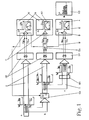
- the sequence of the measurement method according to the invention for determining small light absorptions is subdivided into three process stages a, b, c.
- preliminary stage a a basic measurement is carried out without the material MA to be examined in order to determine the actual state of the measuring arrangement.
- tuning stage b a zero deviation that may have been found in the preliminary stage a is then tuned.
- measurement stage c the actual measurement series is carried out.
- the three process stages a, b, c are shown in chronological order. Intensities I M , I R that occur are plotted over the measuring time t in small diagrams which are intended to illustrate the relationships.
- a measuring light beam M with a selected measuring wavelength ⁇ M and a basic intensity I Ma dependent on the generation source and a reference light beam R with a selected reference wavelength ⁇ R and a basic intensity I Ra likewise dependent on the generating source are used for a detection DE fed.
- measuring and reference light beams M, R can appear as individual beams or together. This is indicated in FIG. 1 by a superordinate beam path S, in which the measuring and reference light beams M, R are contained.
- the detection DE of the basic intensities I Ma and I Ra can take place quasi-simultaneously with the rapidly alternating supply of measuring and reference light beams M, R or exactly at the same time with simultaneous supply.
- the detection DE produces a measurement signal U Ma and a reference signal U Ra . These are fed to an analog common detection E.
- This common detection E takes the form of a difference D between the measurement and reference signal U Ma , U Ra .
- an intensity difference ⁇ I between the intensities I Ma , I Ra is displayed as a directly measured light absorption LA with an analog display device A.
- no light absorption LA can occur since there is no absorbent material MA in the beam path S.
- the displayed intensity difference ⁇ I is therefore a natural intensity difference ⁇ I N between the measurement and reference light beam M, R, which has its cause in the different wavelengths ⁇ m , ⁇ R and for a different weighting of the measurement and reference light beam M, R leads. If this difference ⁇ I N were not taken into account, it would falsify each measurement result, so that the values displayed on the analog display device A did not allow a quick and direct statement about the measured light absorption LA. Therefore, in the measuring method, the natural intensity difference ⁇ I N is automatically taken into account in the form of an adjustment AN of the difference formation D to zero. As a result, each subsequent measurement result displayed with the analog display device A can now be interpreted as directly measured light absorption LA without additional preparation.
- the reconciliation AN of the difference formation D to zero takes place in a reconciliation measurement in the reconciliation stage b.
- Optical zeroing OA or electronic zeroing EA can be performed. This alternative is shown in FIG. 1 by the dashed lines of action when forming the difference D in the preliminary stage a. However, only one of the two voting options is carried out, both of which achieve the same effect.
- the basic intensity I Ra of the reference light beam R is greater than the basic intensity I Ma of the measuring light beam M.
- the balancing is not carried out optically but electronically with the electronic zero adjustment EA.
- the weighting can be set, for example, by a computer-controlled change in amplification factors when forming the difference D.
- this adjustment AN can also largely compensate for matrix effects.
- a substrate disk (without an absorbing layer) or a solvent (without the substance to be analyzed), which may falsify the measurement result is introduced into the beam path S and the intensity difference ⁇ I is adjusted to zero.
- the natural difference in intensity ⁇ I N is always neutralized by its automatic consideration B in its influence on the measurement result.
- the actual measurement can now be carried out in measuring stage c.
- the material MA to be examined is introduced into the beam path S, so that the measurement and reference light beam M, R transmit.
- the measuring light beam M is optimally absorbed by the material MA due to its measuring wavelength ⁇ M , which was selected above the absorption edge or in the range of an absorption band of the material MA. Furthermore, it is weakened by additional interference, in particular reflection and scattering. Its basic intensity I Ma decreases to the transmission intensity I Mc .
- the reference light beam R has the reference wavelength ⁇ R , which is selected in the transparent spectral range of the material to be examined MA close to the measurement wavelength ⁇ M. It is therefore only insignificantly absorbed by the material MA, but is mainly subject to the interferences that occur. Its tuning intensity I Rb (with optical tuning OA; I Ra with electronic tuning EA) lowers to the transmission intensity I Rc , which is in any case even greater than the transmission intensity I Mc of the measuring light beam M.
- the subsequent detection DE then results the measurement and reference signals U Mc and U Rc (with optical tuning OA; U Ra with electronic tuning EA). These are now fed to the analog difference formation D, taking into account B the natural intensity difference ⁇ I N automatically.
- the quick and highly precise measurement result of this difference formation D as a directly measured value is the light absorption LA by the material MA to be examined. All disturbing influences were largely compensated for when forming the difference D.
- the measurement results of the light absorptions LA can then be processed, for example, in a graphical representation GD.
- the presentation can be continuous or discreet depending on the type of detection DE, as well as location-independent over the entire measuring time t or depending on the measuring location x depending on the type of material MA to be examined.
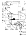
- FIG. 2 shows a particularly preferred embodiment for carrying out the measuring method in schematic form. It is characteristic of this embodiment that it has a single light source 20 and two detectors 21, 22. The detection DE thus takes place exactly at the same time.
- the material MA to be examined is a solid, the thickness of which is to be determined by measuring the light absorption LA.
- the solid is an epitaxial semiconductor chip 23 with an absorbent InGaAsP layer 24, which has grown epitaxially on a transparent InP layer 25.
- the absorbent layer 24 has a thickness between 0.01 and 2 ⁇ m
- the transparent layer 25 has a thickness of around 300 ⁇ m.
- a common beam path S is first passed through a first converging lens 26, then through a spatial filter 27 and then through a second converging lens 28 for better beam focusing.
- the spatial filter 27 represents a replacement for light sources and, with its strong diaphragm, serves to improve beam focusing for a highly precise measurement location resolution.
- a rotating chopper 29 is arranged behind the spatial filter 27 and clocks the beam path S as alternating light, in the example with a frequency f of 1 kHz.
- the beam path S falls on a deflecting mirror 30 and from there through a third converging lens 31 on the semiconductor chip 23, which is arranged on a measuring table 32 which can be moved in two directions x, y.
- a focusing point 33 lies on the upper side 24 of the semiconductor chip 23 due to the smooth rear side 25. In the case of a solid to be examined with a rough rear side, the focusing point 33 would lie on this rough rear side in order to be able to detect the scattered light as completely as possible.
- the diameter of the focusing point 33 depends on the quality of the beam path S and can be 100 ⁇ m and less with good accuracy.
- a fourth converging lens 34 for parallelizing the beam is arranged behind the semiconductor chip 23 and has a large aperture corresponding to the scattering angle of the scattered light that occurs. Behind this fourth converging lens 34, the beam path S is directed to a beam splitter 35, which splits the beam path S into two individual beams 36, 37. Because of the zero adjustment, the division ratio of the beam splitter 35 is not of interest, it is automatically taken into account.
- the measuring light beam M with the measuring wavelength ⁇ M is filtered out of the single beam 36 deflected by the beam splitter 35 using a measuring wavelength filter 38. This is chosen in accordance with the band edge of the absorbing InGaAsP layer 24 of the semiconductor chip 23 so that the measuring light beam M is absorbed to a maximum.
- the single beam 37 passing through the beam splitter 35 is passed through a reference wavelength filter 39, whereby the reference light beam R with the reference wavelength ⁇ R is selected.
- the reference wavelength ⁇ R is selected in the transparent spectral range of the InGaAsP layer 24 in the vicinity of the band edge so that the light absorption LA is only minimal. Therefore, the reference light beam R is mainly weakened by the interference effects during transmission through the semiconductor chip 23.
- the natural difference in intensity ⁇ I N (see Fig. 1) between the measurement and reference light beam M, R is automatically compensated for by an optical tuning OA.
- a variable gray filter 40 is arranged in the reference light beam R. The position of this can be changed manually using a micrometer screw or by means of a computer control.
- the reference light beam R is then passed through a fifth converging lens 41 onto the first detector 21.
- the measuring light beam M falls on the second detector 22 without further influence by a sixth converging lens 42.
- the absolutely simultaneous detection DE with the detectors 21, 22 is made possible by the arrangement described that the one light beam S is optically split and off after the material transmission the resulting individual beams 35, 36 measuring and reference light beams M, R are filtered out.
- Each of the two detectors 21, 22, which are InGaAs or Ge photodiodes in the example, is connected to an electrical preamplifier 43, 44, which converts the photocurrent generated by the detectors 21, 22 into the measurement and reference signal U M , Convert U R in the form of voltages.
- an electronic adjustment can also be carried out by computer-controlled variation of their amplification factors.
- the generated measurement and reference signals U M , U R are then fed to an analog common detection E in the form of a differential amplifier 45, which forms the signal difference ⁇ U from the analog individual signals U M , U R as a measure of the light absorption LA sought. Since this signal difference ⁇ U is very small, it can be measured with high resolution accuracy.
- the differential amplifier 45 is a first lock-in amplifier 46 with which frequency and phase-selective suppression of general interference influences can be. Only the desired measurement and reference signals U M , U R are processed by this first lock-in amplifier 46 on the basis of their alternating frequency f impressed with the chopper 29. With a second lock-in amplifier 47, the reference signal U R is measured simultaneously with the analog difference ⁇ U.
- Both measurands ⁇ U, U R are required to calculate the layer thickness.
- this calculation is carried out using a computer 48 (Atari, VME bus, Rhotron).
- the measuring table 32 and the variable gray filter 40 are also controlled with this computer 48 and a necessary calibration is carried out.
- the computer 48 can also take control of the pre-amplification factors.
- the calculated layer thicknesses are then forwarded to a plotter 49, with which a three-dimensional layer thickness mapping is produced by the semiconductor chip 23 in the example.
- a separate, direct representation of the absorption values (GD; see FIG. 1) determined analogously is not provided in this exemplary embodiment.
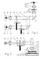
- FIG. 3 schematically shows an embodiment for carrying out the measuring method, which essentially differs from the exemplary embodiment in FIG. 2 in that only a single detector 60 is used.
- the detection DE thus takes place quasi-simultaneously.
- the elements that correspond to the optical structure in FIG. 2 are provided with the same reference symbols and are not explained further here.
- the first individual beam 36 is guided parallel to the second individual beam 37 by a further deflecting mirror 61.
- Measuring and reference light beam M, R are clocked together alternately with a first chopper 62 at a first frequency f1, and the reference light beam R with a second chopper 63 in one second frequency f2 additionally clocked.
- the first clocking with the frequency f1 has the effect that the measurement and reference light beam M, R are passed quickly and alternately via a further converging lens 64 to the one detector 60.
- An additional optical coupling of the reference light beam R into the beam path of the measuring light beam M is required for this purpose.
- the single detector 60 therefore detects measuring and reference light beams M, R alternately in the first frequency f1 and only the reference light beam R in the second frequency f2.
- the detected measurement and reference signals U M , U R are then fed to a single preamplifier 67. Since the signals U M , U R are only processed with one detector 60 and one preamplifier 67, a possible drift between a plurality of detectors and preamplifiers is avoided.
- the automatic consideration B of the natural intensity difference ⁇ I N takes place exclusively through the optical tuning OA. Because of the different modulation, the difference ⁇ U is then formed from the measurement and reference signal U M , U R with the first lock-in amplifier 46 and the differential amplifier 45, the first lock-in amplifier 46 being connected via a line 68 to the Frequency f1 of the first chopper 62 is correlated.
- the reference signal U R is additionally provided with the second lock-in amplifier 47.
- the second lock-in amplifier 47 is correlated with the frequency f2 of the second chopper 63 via a line 69.
- the evaluation is carried out via the computer 48.
- Control lines 70, 71 for the automatic control of the measuring table 32 and the variable gray filter 40 for optical tuning OA are also shown.
- FIG. 4 shows a section of a measuring arrangement for the method, which differs from the two previous exemplary embodiments in FIGS. 2 and 3 in the generation of measuring and reference light beams M, R.
- these are generated by filtering them out of two individual beams, which result from the optical division of a single light beam from a light source.
- measuring and reference light beams M, R are generated directly by means of two monochromatic light sources.
- these are two power-stabilized laser diodes 80, 81 with the wavelengths ⁇ M and ⁇ R selected in accordance with the material to be examined MA.
- electronic tuning EA is possible by regulating the power of the corresponding laser diode 80, 81 (not shown).
- the further beam path of the measuring and reference light beam M, R essentially corresponds to that from FIG. 3.
- the measuring and reference light beam M, R are guided via converging lenses 82, 83 for further focusing and then alternately clocked at a frequency f3 by a chopper 84 .
- the frequency f4 is also impressed on the reference light beam R with a second chopper 85. Since the laser diodes 80, 81 used also produce very stable output signals in alternating operation, the mechanical choppers 84, 85 can also be replaced by electrical modulation (not shown).
- the two laser diodes 80, 81 are switched on and off alternately.
- the reference light beam R is first passed over a deflection mirror 86 and then over a beam splitter 87.
- both beams M, R are pivoted in their direction by 90 °, for example for reasons of space, via a further deflecting mirror 88.
- a collecting lens 89.90 is again provided in front of and behind the material MA to be examined.
- the material MA to be examined is displaceable in the directions x, y by a measuring table (32; see FIG. 3), not shown.
- the detection DE is carried out by a single detector 91, which can be identical to the detector 60 from FIG. 3.
- the further structure behind the detector 91 corresponds to that in FIG. 3 and is therefore not shown here.
- the automatic consideration of the natural intensity difference I N is also not shown. This can be done in the manner already described by optical tuning (OA; see Fig. 2) by weakening the corresponding light beam in front of the chopper 84 or by electronic tuning (EA; see Fig. 2) by means of power regulation of the corresponding laser diode 80 , 81
- the section of an arrangement for carrying out the method shown in FIG. 5 essentially corresponds to the structure described in FIG. 2, the only difference being that the detection DE (only indicated in FIG. 5) is on an incident side 100 of the material to be examined MA is done. Because of the other agreement, the details already described are identified by the same reference numerals as in FIG. 2; The structure of detection, detection, tuning and evaluation, not shown in FIG. 5, is identical to that in FIG. 2 and is not explained in more detail here.
- FIG. 5 shows an incident light arrangement for a solid body. However, this arrangement can also be used, for example, for process monitoring of liquid or gaseous media. It is essential that the material to be examined MA, in the selected exemplary embodiment an absorbent layer 101 of a solid should be determined in its thickness, has a reflector 104 on its rear side 102, which is formed by a transparent substrate 103. In the example shown, this is a metal carrier firmly connected to the transparent substrate 103. However, it can also be a vapor-deposited metal contact (e.g. made of Au) or an external mirror.
- a vapor-deposited metal contact e.g. made of Au
- the beam path S is directed via a semitransparent mirror 105 onto the material MA to be examined. It is reflected on the reflector 104, then passes through the mirror 105 and is fed to the detection DE in the manner already described (FIG. 2).
- the illumination by the light source 20 and the detection DE are therefore both on the incident light side 100 of the material MA to be examined, which also means space savings.
- the measuring light beam M is weakened twice by the absorbing layer 101 and that the intensity I Rc (see FIG. 1) of the reference light beam R to be detected has two reflection components due to reflection the surface of the absorbent layer 101 and on the reflector 104.
- the reflection component on the surface of the absorbing layer 101 is unknown, this can be excluded from the detection DE by illuminating the material MA according to the dark field principle.
- the arrangement based on this principle is not shown in FIG. 5, but will be briefly explained here, since it differs from the illustrated arrangement only in details.
- the beam path S is directed onto the material MA to be examined via a very small deflecting mirror (instead of a semitransparent mirror 105).
- a large deflecting mirror with a small hole and an exchange of light source 20 and detection DE is also possible.
- the incidence of light is perpendicular to the material MA and is focused on the surface of the absorbent layer 101.
- the portion of light reflected on the surface is returned exactly in the beam path S via the small deflecting mirror to the light source 20. It does not get into the detection beam path.
- parallel light beams strike the material MA to be examined, for example by arranging the small deflecting mirror between the fourth converging lens 34 and the material MA to be examined.
- the light component passing through the absorbing and transparent layers 101, 103 is reflected on the reflector 104. This is opaque, so that the light component is reflected in a large solid angle (the same effect is also caused by a rough, scattering back of the material to be examined MA).
- the reflected light is then detected by the fourth converging lens 34, which has a correspondingly large aperture, and is guided past the small deflecting mirror into the detection beam path for detection DE. Then again when evaluating to take into account the double absorption of the detected light component.
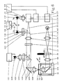
- FIG. 6 shows an arrangement example for the combination of the measurement method for small light absorptions with the luminescence method known per se.
- this method is only explained in principle in order to establish the connection, essential for the invention is the coupling of the two methods, which is a clear improvement with regard to the course and duration of the method by adjusting the material to be examined MA only once and by assigning the material parameters measured with the two methods at identical sample points.
- the reference symbols used in FIG. 2, insofar as the arrangement parts are identical, are adopted.
- the luminescence method is used to determine characteristic properties of semiconductor materials, in particular the band edge (absorption edge).
- the band edge In technologically important mixed crystals such as InGaAsP or GaAlAs, the band edge can be adjusted using the mixing ratio.
- the band edge is one of the most important design parameters in optoelectronic components. This parameter can be determined from luminescence emission spectra. It is important for the measuring method for the determination of small light absorptions that the measuring wavelength is optimally chosen from knowledge of the band edge and that the absorption coefficient of the layer to be examined in each case can be derived at this measuring wavelength.
- the absorbing layer 24 of the material to be examined MA is irradiated with monochromatic light from a laser diode 120, which is fed from a power supply 121.
- the beam path S of the light runs through a first converging lens 122, a color filter 123 for filtering out background interference, a dichroic one Mirror 124, a deflecting mirror 125 and a second converging lens 126.
- the material MA is excited by the light to emit characteristic radiation (luminescence effect). This emitted luminescence radiation is in turn fed to the dichroic mirror 124 via the deflection mirror 125. This has the property that it either reflects or lets light pass depending on its wavelength.
- the luminescence radiation is imaged with a third converging lens 128 into a tunable monochromator 129.
- the wavelength of the monochromator 129 is varied with a motorized adjustment 130.
- the spectrally selected light is imaged behind the monochromator 129 with a fourth converging lens 131 onto a detector 132 and the emission spectrum is recorded with it.
- a second deflection mirror 133 can be introduced into the beam path S in front of the monochromator 129 and the integral luminescence - an important measure of the crystal quality - can thus be measured with a further detector 134.
- the signals from the detectors 132, 134 are fed to differential inputs of a lock-in amplifier 135, the detector 132, 134 not required in each case being short-circuited via a switch 136.
- the control of the wavelength adjustment 130 and the measuring table 32 via a stepper motor 137 are carried out by a computer 138. This is also used for evaluation.
- the measuring method for determining small light absorptions LA is now coupled into the described structure for the luminescence measuring method as follows:
- the beam path S emanating from the light source 20 is initially already in Described way on an arrangement of fifth lens 139, spatial filter 27, chopper 29 and sixth lens 140 directed to a third deflection mirror 141.
- This directs the beam path S via a seventh converging lens 142 onto the material MA to be examined.
- the beam path S is guided through the second converging lens 126, the deflecting mirror 125, the dichroic mirror 124, which in the example shown does not allow only the wavelength of the light from the laser diode 120 to pass through, the color filter 127 and the third converging lens 128.
- a beam splitter 143 is now introduced into the beam path. This splits the light beam S into a first partial light beam 144 and a second partial light beam 145. The reflected first partial light beam 144 is then filtered by the now inserted reference wavelength filter 39, so that the reference light beam R is created.
- the monochromator 129 is set to the measuring wavelength ⁇ M , and the measuring light beam M is filtered out of the second partial light beam 130. Measuring and reference light beam M, R are then detected simultaneously with detectors 132 and 134, and measuring and reference signal U M , U R are fed to difference formation D.
- the switch 136 is in a zero position and does not short either of the two detectors 132, 134. To obtain the reference signal U R , the detector 132 can either be short-circuited for a short time via the switch 136 or the reference signal U R is passed in parallel to a second lock-in amplifier (not shown) in order to achieve a high measuring speed.
- Differential signal ⁇ U and reference signal U R are - as already stated - necessary to calculate the layer thickness of the material to be examined MA from the measured small light absorptions.
- the automatic consideration B of the natural intensity difference ⁇ I N required for the direct measurement of the small light absorptions takes place in the arrangement shown for the coupled Execution of both measuring methods by the electronic coordination EA when forming the difference D.
Applications Claiming Priority (2)
| Application Number | Priority Date | Filing Date | Title |
|---|---|---|---|
| DE4005864 | 1990-02-22 | ||
| DE4005864 | 1990-02-22 |
Publications (2)
| Publication Number | Publication Date |
|---|---|
| EP0443702A2 true EP0443702A2 (fr) | 1991-08-28 |
| EP0443702A3 EP0443702A3 (en) | 1993-12-15 |
Family
ID=6400889
Family Applications (1)
| Application Number | Title | Priority Date | Filing Date |
|---|---|---|---|
| EP19910250052 Withdrawn EP0443702A3 (en) | 1990-02-22 | 1991-02-22 | Measuring method for determining small light absorptions |
Country Status (3)
| Country | Link |
|---|---|
| US (1) | US5185645A (fr) |
| EP (1) | EP0443702A3 (fr) |
| JP (1) | JPH0518896A (fr) |
Cited By (1)
| Publication number | Priority date | Publication date | Assignee | Title |
|---|---|---|---|---|
| WO1996025645A1 (fr) * | 1995-02-16 | 1996-08-22 | Wissenschaftlich-Technisches Optikzentrum Nordrhein-Westfalen (Optikzentrum Nrw) E.V. | Dispositif de determination de l'epaisseur de couches colorees sur des supports transparents |
Families Citing this family (12)
| Publication number | Priority date | Publication date | Assignee | Title |
|---|---|---|---|---|
| US5923430A (en) * | 1993-06-17 | 1999-07-13 | Ultrapointe Corporation | Method for characterizing defects on semiconductor wafers |
| US5363171A (en) * | 1993-07-29 | 1994-11-08 | The United States Of America As Represented By The Director, National Security Agency | Photolithography exposure tool and method for in situ photoresist measurments and exposure control |
| US5381010A (en) * | 1993-12-03 | 1995-01-10 | Sleepair Corporation | Periodically alternating path and alternating wavelength bridges for quantitative and ultrasensitive measurement of vapor concentration |
| EP1322908A1 (fr) * | 2000-10-05 | 2003-07-02 | Opnetics Corporation | Systeme de commande et de suivi d'indice de refraction et d'epaisseur in-situ pour depot de couche mince |
| CN101147054B (zh) * | 2005-04-28 | 2011-06-08 | 丰田自动车株式会社 | 排气分析装置 |
| US7609380B2 (en) * | 2005-11-14 | 2009-10-27 | Schlumberger Technology Corporation | Real-time calibration for downhole spectrometer |
| JP4199766B2 (ja) * | 2005-12-16 | 2008-12-17 | トヨタ自動車株式会社 | 排ガス分析方法および排ガス分析装置 |
| JP4732277B2 (ja) * | 2006-08-23 | 2011-07-27 | トヨタ自動車株式会社 | ガス分析装置及びガス分析方法 |
| ES2597456T3 (es) * | 2008-02-15 | 2017-01-18 | The Science And Technology Facilities Council | Espectrómetro infrarrojo |
| US10197545B2 (en) * | 2015-07-29 | 2019-02-05 | Advanced Sensors Limited | Method and apparatus for measurement of a material in a liquid through absorption of light |
| DE102018103171A1 (de) * | 2017-11-23 | 2019-05-23 | Tdk Electronics Ag | Verfahren zum Bestimmen von Eigenschaften einer Beschichtung auf einer transparenten Folie, Verfahren zur Herstellung einer Kondensatorfolie und Einrichtung zum Bestimmen von Eigenschaften einer Beschichtung auf einer transparenten Folie |
| US11035728B2 (en) * | 2018-08-08 | 2021-06-15 | Picarro, Inc. | Cavity ring-down spectroscopy having interleaved data acquisition for interference mitigation |
Citations (6)
| Publication number | Priority date | Publication date | Assignee | Title |
|---|---|---|---|---|
| FR2314493A1 (fr) * | 1975-06-12 | 1977-01-07 | Measurex Corp | Procede et appareil de mesure de la quantite d'une matiere etrangere telle que l'eau portee par une feuille |
| US4191940A (en) * | 1978-01-09 | 1980-03-04 | Environmental Research Institute Of Michigan | Method and apparatus for analyzing microscopic specimens and the like |
| WO1981002633A1 (fr) * | 1980-03-06 | 1981-09-17 | Baxter Travenol Lab | Dispositif et procede photometriques |
| EP0087077A2 (fr) * | 1982-02-23 | 1983-08-31 | Siemens Aktiengesellschaft | Dispositif pour la mesure optique de gaz |
| EP0303132A2 (fr) * | 1987-08-10 | 1989-02-15 | Fresenius AG | Détecteur d'hémoglobine |
| EP0401453A1 (fr) * | 1989-05-23 | 1990-12-12 | Biosensors Technology, Inc. | Méthode pour déterminer, par absorbtion de rayonnement, la concentration de substances dans des matrices absorbantes et troubles |
Family Cites Families (6)
| Publication number | Priority date | Publication date | Assignee | Title |
|---|---|---|---|---|
| US3332313A (en) * | 1962-04-02 | 1967-07-25 | Du Pont | Apparatus for absorption spectra analysis |
| US3910701A (en) * | 1973-07-30 | 1975-10-07 | George R Henderson | Method and apparatus for measuring light reflectance absorption and or transmission |
| JPS583073Y2 (ja) * | 1975-07-19 | 1983-01-19 | 株式会社島津製作所 | ブンコウコウドケイ |
| FR2474166A1 (fr) * | 1980-01-23 | 1981-07-24 | Commissariat Energie Atomique | Dispositif de mesure photometrique pour solutions complexes a bruit de fond variable |
| DE3407850A1 (de) * | 1984-02-29 | 1985-09-05 | Hahn-Meitner-Institut für Kernforschung Berlin GmbH, 1000 Berlin | Mikrowellen-messverfahren und -messapparatur zur kontaktlosen und zerstoerungsfreien untersuchung photoempfindlicher materialien |
| JPH0315742A (ja) * | 1989-03-23 | 1991-01-24 | Anritsu Corp | ガス検出装置 |
-
1991
- 1991-02-21 US US07/659,008 patent/US5185645A/en not_active Expired - Fee Related
- 1991-02-21 JP JP3027313A patent/JPH0518896A/ja active Pending
- 1991-02-22 EP EP19910250052 patent/EP0443702A3/de not_active Withdrawn
Patent Citations (6)
| Publication number | Priority date | Publication date | Assignee | Title |
|---|---|---|---|---|
| FR2314493A1 (fr) * | 1975-06-12 | 1977-01-07 | Measurex Corp | Procede et appareil de mesure de la quantite d'une matiere etrangere telle que l'eau portee par une feuille |
| US4191940A (en) * | 1978-01-09 | 1980-03-04 | Environmental Research Institute Of Michigan | Method and apparatus for analyzing microscopic specimens and the like |
| WO1981002633A1 (fr) * | 1980-03-06 | 1981-09-17 | Baxter Travenol Lab | Dispositif et procede photometriques |
| EP0087077A2 (fr) * | 1982-02-23 | 1983-08-31 | Siemens Aktiengesellschaft | Dispositif pour la mesure optique de gaz |
| EP0303132A2 (fr) * | 1987-08-10 | 1989-02-15 | Fresenius AG | Détecteur d'hémoglobine |
| EP0401453A1 (fr) * | 1989-05-23 | 1990-12-12 | Biosensors Technology, Inc. | Méthode pour déterminer, par absorbtion de rayonnement, la concentration de substances dans des matrices absorbantes et troubles |
Cited By (1)
| Publication number | Priority date | Publication date | Assignee | Title |
|---|---|---|---|---|
| WO1996025645A1 (fr) * | 1995-02-16 | 1996-08-22 | Wissenschaftlich-Technisches Optikzentrum Nordrhein-Westfalen (Optikzentrum Nrw) E.V. | Dispositif de determination de l'epaisseur de couches colorees sur des supports transparents |
Also Published As
| Publication number | Publication date |
|---|---|
| US5185645A (en) | 1993-02-09 |
| JPH0518896A (ja) | 1993-01-26 |
| EP0443702A3 (en) | 1993-12-15 |
Similar Documents
| Publication | Publication Date | Title |
|---|---|---|
| EP0143282B1 (fr) | Procédé pour la mesure sans contact de la température d'un objet par mesure du rayonnement sans influence du degré d'émissivité | |
| DE3003533C2 (de) | Vorrichtung zur Bestimmung der gegenseitigen Lagebeziehung zwischen zwei Prüflingen | |
| DE4223337C2 (de) | Verfahren und Anordnung zur photothermischen Spektroskopie | |
| EP3658896B1 (fr) | Procédé d'examen spectroscopique et/ou spectrométrique d'un échantillon et dispositif interférométrique | |
| DE102005049175B4 (de) | Infrarotgasanalysator und Verfahren zur Infrarotgasanalyse | |
| DE19511869A1 (de) | Verfahren und Anordnung zur Responseanalyse von Halbleitermaterialien mit optischer Anregung | |
| DE102007052551A1 (de) | Konfiguration eines Laser-Scanning -Mikroskops für eine Rasterbildkorrelationsspektroskopiemessung sowie Verfahren zur Durchführung und Auswertung einer solchen Messung | |
| DE2362935A1 (de) | Anordnung zur ueberwachung der luftverunreinigung | |
| EP0443702A2 (fr) | Procédé de mesure pour déterminer de petites absorptions de lumière | |
| DE2438294B2 (de) | Infrarotgasanalysator | |
| EP0244721B1 (fr) | Procédé et système pour mesurer la transmission optique | |
| EP0283047A2 (fr) | Procédé et dispositif pour l'obtention sans contact de données pour déterminer la résolution spatiale de la densité et de la température dans un volume de mesure | |
| EP2985592A1 (fr) | Spectromètre à absorption et procédé destiné à mesurer la concentration d'un composant gazeux pertinent d'un gaz de mesure | |
| DE4035266A1 (de) | Verfahren und anordnung zur thermowellenanalyse | |
| EP0145877A2 (fr) | Photomètre pour l'analyse en continu d'un milieu (gaz ou liquide) | |
| DE2358590C3 (de) | Atomabsorptionsspektrophotometer | |
| DE4122572A1 (de) | Verfahren zum betrieb einer laserdiode | |
| EP0218213B1 (fr) | Procédé et dispositif pour la mesure en ligne de la transmission ou réflexion de rayonnement électromagnétique par des objets en mouvement | |
| DE102012005428A1 (de) | Vorrichtung zum Bestimmen der Temperatur eines Substrats | |
| DE3215249C2 (de) | Photometer zur Messung der Atomfluoreszenz | |
| EP0685729A1 (fr) | Procédé spectroscopique de mesure des absorptions très faibles | |
| DE112017008083B4 (de) | Ferninfrarotlichtquelle und ferninfrarotspektrometer | |
| DE2417427A1 (de) | Fluoreszenz-spektralphotometer | |
| DE2511570A1 (de) | Spektrofluorometer | |
| DE4106042A1 (de) | Messverfahren zur bestimmung kleiner lichtabsorptionen |
Legal Events
| Date | Code | Title | Description |
|---|---|---|---|
| PUAI | Public reference made under article 153(3) epc to a published international application that has entered the european phase |
Free format text: ORIGINAL CODE: 0009012 |
|
| AK | Designated contracting states |
Kind code of ref document: A2 Designated state(s): BE CH DE ES FR GB IT LI NL |
|
| PUAL | Search report despatched |
Free format text: ORIGINAL CODE: 0009013 |
|
| AK | Designated contracting states |
Kind code of ref document: A3 Designated state(s): BE CH DE ES FR GB IT LI NL |
|
| STAA | Information on the status of an ep patent application or granted ep patent |
Free format text: STATUS: THE APPLICATION IS DEEMED TO BE WITHDRAWN |
|
| 18D | Application deemed to be withdrawn |
Effective date: 19940301 |