EP0440908A2 - Technik zur Adressengenerierung während eines Befehlsdekodierungszyklus in einem RISC-Prozessor - Google Patents
Technik zur Adressengenerierung während eines Befehlsdekodierungszyklus in einem RISC-Prozessor Download PDFInfo
- Publication number
- EP0440908A2 EP0440908A2 EP90122945A EP90122945A EP0440908A2 EP 0440908 A2 EP0440908 A2 EP 0440908A2 EP 90122945 A EP90122945 A EP 90122945A EP 90122945 A EP90122945 A EP 90122945A EP 0440908 A2 EP0440908 A2 EP 0440908A2
- Authority
- EP
- European Patent Office
- Prior art keywords
- instruction
- address
- register
- current instruction
- risc
- Prior art date
- Legal status (The legal status is an assumption and is not a legal conclusion. Google has not performed a legal analysis and makes no representation as to the accuracy of the status listed.)
- Withdrawn
Links
Images



Classifications
-
- G—PHYSICS
- G06—COMPUTING OR CALCULATING; COUNTING
- G06F—ELECTRIC DIGITAL DATA PROCESSING
- G06F9/00—Arrangements for program control, e.g. control units
- G06F9/06—Arrangements for program control, e.g. control units using stored programs, i.e. using an internal store of processing equipment to receive or retain programs
- G06F9/30—Arrangements for executing machine instructions, e.g. instruction decode
- G06F9/38—Concurrent instruction execution, e.g. pipeline or look ahead
- G06F9/3818—Decoding for concurrent execution
- G06F9/382—Pipelined decoding, e.g. using predecoding
-
- G—PHYSICS
- G06—COMPUTING OR CALCULATING; COUNTING
- G06F—ELECTRIC DIGITAL DATA PROCESSING
- G06F9/00—Arrangements for program control, e.g. control units
- G06F9/06—Arrangements for program control, e.g. control units using stored programs, i.e. using an internal store of processing equipment to receive or retain programs
- G06F9/30—Arrangements for executing machine instructions, e.g. instruction decode
- G06F9/30145—Instruction analysis, e.g. decoding, instruction word fields
-
- G—PHYSICS
- G06—COMPUTING OR CALCULATING; COUNTING
- G06F—ELECTRIC DIGITAL DATA PROCESSING
- G06F9/00—Arrangements for program control, e.g. control units
- G06F9/06—Arrangements for program control, e.g. control units using stored programs, i.e. using an internal store of processing equipment to receive or retain programs
- G06F9/30—Arrangements for executing machine instructions, e.g. instruction decode
- G06F9/30145—Instruction analysis, e.g. decoding, instruction word fields
- G06F9/3016—Decoding the operand specifier, e.g. specifier format
- G06F9/30167—Decoding the operand specifier, e.g. specifier format of immediate specifier, e.g. constants
-
- G—PHYSICS
- G06—COMPUTING OR CALCULATING; COUNTING
- G06F—ELECTRIC DIGITAL DATA PROCESSING
- G06F9/00—Arrangements for program control, e.g. control units
- G06F9/06—Arrangements for program control, e.g. control units using stored programs, i.e. using an internal store of processing equipment to receive or retain programs
- G06F9/30—Arrangements for executing machine instructions, e.g. instruction decode
- G06F9/32—Address formation of the next instruction, e.g. by incrementing the instruction counter
-
- G—PHYSICS
- G06—COMPUTING OR CALCULATING; COUNTING
- G06F—ELECTRIC DIGITAL DATA PROCESSING
- G06F9/00—Arrangements for program control, e.g. control units
- G06F9/06—Arrangements for program control, e.g. control units using stored programs, i.e. using an internal store of processing equipment to receive or retain programs
- G06F9/30—Arrangements for executing machine instructions, e.g. instruction decode
- G06F9/38—Concurrent instruction execution, e.g. pipeline or look ahead
- G06F9/3824—Operand accessing
- G06F9/383—Operand prefetching
Definitions
- the invention relates to apparatus and accompanying methods, particularly suited for use in conjunction with pipelined instruction processing occurring in a processor of a reduced instruction set computer (RISC), for substantially eliminating a wait state, heretofore frequently caused by an address generation cycle occurring during RISC instruction processing, by generating an address during a decode cycle of this processing.
- RISC reduced instruction set computer
- compilers have been and are used to translate relatively high level programs into corresponding sequences of instructions (low level machine code) for subsequent execution on a computer.
- compiled machine code should be as efficient as possible, i.e. it should invoke no wasted operations. Each wasted operation unnecessarily consumes processing time and/or computer resources.
- a compiler that generates CISC machine code often does not generate an efficient sequence of CISC instructions for a given statement in a high level program. This occurs as the result of the nature of CISC instruction sets.
- an efficient sequence of CISC instructions which takes advantage of the instruction processing pipeline used in a CISC processor, is not possible.
- each CISC instruction is a combination of two or more simpler RISC-like instructions.
- only certain combinations of these simpler instructions are actually supported by the architecture of a CISC processor. Accordingly, an optimum combination of the simpler RISC-like instructions is not possible in all cases, even with perfect compilers.
- a finer-grained instruction set such as that for RISC
- a compiler which produces machine code for that instruction set has both an easier job and hence a improved chance of generating a more optimum sequence of operations which are tailored to the specific instruction processing pipeline used in the processor that executes that set than does a compiler that generates CISC machine code.
- microcomputer systems suffer the same limitations on processing speed engendered by the use of sophisticated multi-layered instruction decoding as occurs in mainframe computers.
- microcomputers With the increasing use of microcomputers to perform sophisticated real-time application processing, such as computer- aided-design and/or engineering tasks or complex numerical analysis or graphics processing, a continuing and growing need exists to increase the processing speed of microcomputer based systems.
- RISC reduced instruction set computers
- the machine code for a program written for a RISC processor usually requires slightly more instructions and hence memory space than does the same program written for a CISC processor; however, available memory space has become much less of an effective limitation on computer design than it was in the past.
- large capacity relatively inexpensive memories such as for example those fabricated through use of currently available cost effective 256 Kbit or 1 Mbit RAM circuits, into a microcomputer system, a substantial number of inexpensive memory locations becomes available for program storage. Accordingly, little need, if any, now exists to reduce program size in order to conserve memory locations.
- fast relatively small optimizing compilers that generate efficient machine code can be more easily written for RISC instructions than for CISC instructions.
- RISC instructions are much simpler to decode than CISC instructions and specifically do not require multi-layered decoding. While a CISC instruction may require several, perhaps as many as three or more, successive machine cycles to fully decode, ideally all instructions in a RISC instruction set should be decodable in only one machine cycle. Accordingly, when both RISC and CISC processors of comparable clock speed are used to execute programs that provide identical functionality, the machine cycles saved in instruction decoding often enable the RISC processor to be much faster than and hence substantially outperform the CISC processor.
- any disadvantages, such as additional memory size and cost, caused by the increased size of a RISC program over its CISC counterpart tend to be clearly outweighed by a significant increase in the speed at which that program can be processed by a RISC processor over that provided by a comparable CISC processor.
- RISC processors employ pipelined instruction processing through which several instructions can be simultaneously processed in a staggered overlapped fashion through the pipeline.
- the pipeline contains separate stages for instruction decoding, address generation, memory access and register loading. Different instructions simultaneously occupy different stages in the pipeline. While any one RISC instruction may require several machine cycles to completely propagate through the pipeline and be fully processed thereby, a new instruction should ideally enter the pipeline, on the average, at every successive machine cycle. However, before certain RISC instructions can be processed, these instructions require the results of their most recently preceding instruction.
- the preceding RISC instruction may not be fully processed and its results made available when a current RISC instruction is ready to be decoded. Accordingly, processing of the current instruction, particularly its instruction decoding, must be delayed, by one and often more machine cycles (through the inclusion of corresponding wait states) until the results of the preceding instruction become available for use. Because, as noted, a new RISC instruction should ideally be processed, on the average, during each successive machine cycle in a RISC processor, even just a one cycle delay (one wait state) that occurs sufficiently frequently in a RISC processor can significantly slow the throughput of that processor.
- RISC instructions that require such delays encompass branch instructions, both unconditional and conditional, which, on the average, occupy one out of every six instructions that execute on a processor. Accordingly, these wait-state delays can indeed occur sufficiently frequently in a program to adversely impact its processing speed.
- a RISC instruction is both fully decoded and pre-decoded in parallel.
- the pre-decoding is used to extract the displacement field from the instruction, select a proper base address for the current RISC instruction and, in conjunction with formatting operations, properly align the displacement field - all within the current decode cycle.
- the base and aligned displacement addresses are then applied to separate inputs of an address adder.
- the output of the adder is propagated through an address register to an output as a memory address during the decode cycle in the event the full instruction decoding confirms that the current RISC instruction does require an address to be calculated; otherwise, the calculated address produced by the adder during this decode cycle is merely discarded by being over-written during a decode cycle for a subsequent RISC instruction.
- our inventive technique first assumes that an address needs to be generated for any current RISC instruction that initially appears to (might possibly) require a memory address (such as illustratively each LOAD or STORE instruction or each branch instruction) regardless of whether that current instruction, when fully decoded, actually requires such an address to be generated or not.
- a pre-decode circuit pre-decodes the operation code (opcode) for the current instruction in order to first extract the displacement address field therefrom, then to format the displacement address field with a proper bit alignment and finally to route the aligned displacement address field to a corresponding input of a binary adder to generate an address.
- the pre-decode circuit also selects the proper source of the base address for the current RISC instruction, illustratively either the contents of an instruction address register (IAR) in the case of branch type RISC instructions that require memory addresses to be generated or general purpose register RC within the GPR array (the exact register being specified by a field in the current instruction itself) in the case of a load or store (referred to as load/store) type RISC instruction that requires an memory address to be generated.
- IAR instruction address register
- RC general purpose register RC within the GPR array
- load/store load/store
- addresses are calculated through use of a separate binary adder rather than through an addition path of an arithmetic logic unit (ALU), these addresses can be calculated in a shorter interval of time, and particular with lessened path delay, than if an ALU were to be used to calculate these addresses.
- ALU arithmetic logic unit
- FIG. 1 depicts a typical RISC instruction 10 that, as part of its processing, requires an address to be generated.
- This address is typically either a branch address or an address of a memory location at which data is to be written into or read from memory.
- the address is usually calculated to be the sum of an address displacement value and the current contents of a given register, with the register and the displacement value both specified within the instruction.
- An illustrative example of instruction 10 is the STORE instruction, STO [R1], [R2] + n, which, when executed, causes the contents of general purpose register R1 to be stored in memory at a memory location given by the sum of the contents of general purpose register R2 (the "base" address) and an address displacement value "n".
- the displacement value is also commonly referred to as either an index or offset value.
- this RISC instruction contains operation code (opcode) field 13, two register fields 15 and 17 and a displacement field 19.
- the opcode field contains appropriate bits that specify the particular data processing operation to be invoked by this instruction.
- Register fields 15 and 17 identify two registers, denoted as R1 and R2, that form part of a group of general purpose registers used during RISC instruction processing.
- Address displacement field 19 contains address displacement value "n".
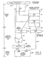
- FIG. 2 depicts the typical multi-cycle processing that occurs in the art for a RISC instruction, specifically a STORE instruction shown in FIG. 1, which requires an address to be generated.
- Instruction processing occurs in a number of processing cycles that collectively spans a succession of consecutive machine cycles. Ideally, each individual processing cycle fully occurs within just one machine cycle.
- these processing cycles collectively encompass an instruction decoding cycle followed by an address generation cycle, succeeded by a memory access cycle, which, in turn, is followed, in the case of an instruction to store data in a register, by a register load cycle.
- RISC instructions typically require three or four successive machine cycles, with the number of cycles being governed by the specific instruction.
- GPR 210 general purpose register array 210
- GPR 210 illustratively contains sixteen different registers. From the instruction, the base address is loaded into register 213, while the data value to be stored within the memory is loaded within register 215.
- address generation cycle 25 occurs. During this cycle, the contents of register R1 are loaded, as symbolized by line 225, into operand register 235. Simultaneously therewith, the base address now residing within register R2 in GPR 210 is loaded, as symbolized by line 223, into base address register 231. Once this occurs, the contents of base address register 231 are applied, as symbolized by line 243, as one input to adder 250. The displacement value "n" contained within instruction register 200 is applied, as symbolized by line 207, to the other input of this adder. The arithmetic logic unit (ALU) of the RISC processor is used to perform the add function symbolized by adder 250.
- ALU arithmetic logic unit
- Adder 250 performs simple binary addition of the base address and the displacement value to generate a memory address.
- the address produced by adder 250 is loaded into address register 260. Once this address has been loaded into the address register, instruction processing continues with memory access cycle 29.
- the address contained within address register 260 is applied, as symbolized by line 265, to an address input of memory 280 which is usually cache or main memory.
- the data value is applied, as symbolized by line 275, to the data input of memory 280.
- the memory undertakes a write operation to store the data value therein.
- RISC instruction has been fully processed and processing for next RISC instruction, which by now resides within instruction register 200, commences.
- the RISC instruction is a LOAD instruction (not shown)
- STORE instruction which requires an address to be generated, such as the contents of a memory location specified by the sum of the contents of register R2 and a displacement value, followed by the loading the contents of this memory location into specified register R1
- memory access cycle 29 would perform a memory read rather than memory write operation and would itself be succeeded by a register load cycle (also not shown).
- register load cycle the contents of the addressed location in memory 280 would be written into specified general purpose register R1. Similar address calculations and multi-cycle instruction processing would also occur during processing of RISC branch instructions.
- RISC processors known in the art employ pipelined instruction processing through which several RISC instructions are simultaneously processed in a staggered overlapped fashion through a pipeline.
- the pipeline contains a separate hardware stage for each different instruction processing cycle: an instruction decoding stage, an address generation stage, a memory access stage and a register loading stage. Because of this pipelined architecture, different RISC instructions can simultaneously occupy different stages in the pipeline. While any one RISC instruction may require several machine cycles to completely propagate through the pipeline and be fully processed thereby, after a well-known multi-cycle (typically two cycle) start-up delay for the RISC pipeline instruction processor has occurred, a new instruction should ideally enter the pipeline, on the average, at every successive machine cycle.
- multi-cycle typically two cycle
- Conditional branches form one illustrative group of these instructions.
- the conditional nature of these instructions necessitates that the results of a prior instruction, which determine whether a condition will be satisfied or not, must be available before a corresponding conditional branch instruction can be fully processed and specifically before a proper branch address can be calculated. Accordingly, processing of the current instruction, particularly its instruction decoding, must be delayed, by one and often more machine cycles until the results of the preceding instruction become available for use.
- a non-branch instruction that involves one of the general purpose registers such as an ADD for adding the contents of two general purpose registers together, may be preceded by an instruction, such as a LOAD, that affects the contents of one of these registers.
- the add operation can not proceed until this one register is loaded with the proper contents.
- processing of a succeeding instruction is halted, by the insertion of an appropriate number of wait states, until the processing of its preceding instruction is completed.
- these wait-state delays if sufficiently frequent, can significantly slow program execution on a RISC processor.
- FIG. 3A diagrammatically shows typical multi-cycle timing associated with pipelined RISC instruction processing, that occurs in the art, for processing two illustrative successive RISC instructions where a first instruction alters the contents of a register and these contents are to be used by a second instruction.
- the first instruction is illustratively a LOAD instruction, specifically LOAD [R1], [R2] + n, that loads general purpose register R1 with a value stored in memory and at a location specified by the sum of the contents of register R2 and displacement value "n".
- This instruction is followed by illustratively an add instruction, specifically ADD [R1], [R3], which adds the contents of general purpose registers R1 and R3 and places the results in an accumulator.
- the LOAD instruction enters the decoding stage of the pipeline with its decoding then occurring during machine cycle T1.
- the LOAD instruction decoding cycle symbolized by line 310 occurs.
- the opcode of the LOAD instruction is decoded and the contents of general purpose registers R1 and R3 are appropriately accessed using address values contained within the instruction.
- LOAD instruction processing passes to the address generation stage of the pipeline at which the LOAD instruction address generation cycle, as symbolized by line 320, occurs.
- the contents of general purpose register R2 and displacement value "n" are added to form a memory address.
- LOAD instruction processing passes to the memory access stage of the pipeline during which the LOAD instruction memory access cycle, as symbolized by line 330, is undertaken to access an addressed memory location. Instruction processing would then proceed to a register load stage, which during machine cycle T 4 -, would ordinarily cause the LOAD instruction register load cycle, as symbolized by line 340, to occur in order to load the contents of the accessed memory location into general purpose register R1.
- GPR 210 is required to permit two of the registers within the GPR array to be simultaneously read while at the same time two other registers within this array are being simultaneously written, for a total of four simultaneously occurring register operations.
- Such a GPR array with this degree of parallelism tends to be disadvantageously complex and expensive, in terms of circuitry area, power required, and processing speed, to implement.
- the need to generate an address and then access memory during processing of the LOAD instruction injected a two cycle delay in the pipelined processing of the ADD instruction. Similar processing delays, due to register locks and decoding cycle inhibition, occur in processing other RISC instructions that require the results generated by processing immediately preceding RISC instructions.
- the interlock circuitry heretofore needed to insert the wait state during the address generation cycle is no longer necessary thereby resulting in simplified pipeline control circuitry - in terms of reduced circuit complexity and reduced size and power requirements.
- the GPR array is only required to be able to simultaneously undertake 2 read operations and 1 write operation rather than 2 read operations and 2 write operations, thereby also simplifying the GPR - again in terms of reduced circuit complexity and reduced size and power requirements.
- LOAD or STORE (after being decoded) instruction occurs while an instruction prefetch buffer is empty, the LOAD or STORE instruction takes precedence, but with only a loss of 1 machine cycle instead of 2 cycles as would occur through use of a separate address generation cycle.
- our inventive technique first assumes that an address needs to be generated during each LOAD or STORE instruction or each branch instruction. Under this assumption, address generation is performed during the decode cycle by a pre-decode circuit that pre-decodes the opcode for each of these instructions to first extract the displacement address field therefrom, then to format the displacement address field into a proper bit alignment and finally to route the aligned displacement address field to a corresponding input of a separate binary adder, rather than the ALU, to generate an address.
- the pre-decode circuit also selects the proper source of the base address for the current RISC instruction: either the contents of an instruction address register (IAR) in the case of branch type RISC instructions that require memory addresses to be generated or a general purpose register RC within the GPR array (as specified by the current instruction itself) in the case of a load or store (collectively referred to herein as load/store) type RISC instruction that requires an memory address to be generated.
- IAR instruction address register
- RC general purpose register RC within the GPR array
- load/store load/store
- a separate binary adder is simpler and significantly faster than the adder portion of an ALU. Consequently, use of such an adder, rather than an ALU in a RISC processor (as well as a serially connected bit formatter) as occurs in the art, to generate an address further increases the speed at which an address can be generated. Moreover, since the output of the binary adder only feeds the address register, this adder has a relatively small load to drive. By contrast, if the ALU were to drive the address register, the ALU would experience a larger load inasmuch as its output is routed to numerous locations, including the GPR array, the address register and elsewhere. Consequently, the path delay associated with use of a separate binary address adder is advantageously likely to be significantly shorter than that associated with use of the ALU as an address adder.
- FIG. 4 specifically depicts these different RISC instruction formats for the IBM PC/RT instruction set.
- IBM PC/RT RISC instruction formats 400 that require an address to be generated encompass both non-branch and branch instructions.
- these instruction formats include: R type instruction format 405 that contains eight-bit opcode field 401 and four-bit operand (RB) and base address (RC) register fields 402 and 403, respectively; R' type instruction format 410 that contains eight-bit opcode field 407 followed by four-bit operand register and four-bit increment (I) fields 408 and 409, respectively; D Short type instruction format 415 that contains four-bit opcode field 411, four-bit (short) increment (Is) field 412, four-bit operand and four-bit base register fields 413 and 414, respectively; X type instruction format 420 that contains four-bit opcode field 416, four-bit result (RA) register field 417, four-bit operand and four-bit base register fields 418 and 419; and D type instruction format 425 that contains eight-bit opcode field 42
- R type (unconditional branch) format 455 that contains eight-bit opcode field 451 followed by four-bit operand and base address register fields 452 and 453
- R" type (conditional branch) format 460 that contains eight-bit opcode field 457, followed by four-bit condition bit number (N) field and four-bit base register field 459
- JI type (conditional branch) format 465 that contains four-bit opcode field 461 followed by four-bit condition bit number field 462 and eight-bit jump immediate (JI) address field 463
- BI' type (conditional branch) format 470 that contains eight-bit opcode field 467, four-bit condition bit number field 468 and twenty-bit branch immediate (BI) address field 469
- BI type (unconditional branch) format 475 that contains eight-bit opcode field 471, four-bit operand register field 472 and twenty-bit branch immediate (BI) address field 473
- FIG. 5 depicts a high level block diagram of apparatus that embodies the teachings of our present invention for generating an address during a decode cycle of RISC instruction processing for illustratively any thirty-two bit RISC instruction.
- a current RISC instruction to be processed is stored in thirty-two bit form, as bits ao, ..., asi, in instruction register 200.
- the opcode of the instruction is routed in parallel, via leads 505, as input to both full decode circuit 510 and instruction pre-decode circuit 520.
- Full decode circuit 510 which is well known and formed through combinatorial logic, fully decodes the instruction and, based upon the decoded opcode and the instruction type, provides a pulse on a corresponding one of the leads within leads 515.
- Leads 515 are connected to the set input of a succession of flip-flops (one bit latches) 560. Each flip-flop is set to a one state if a pulse appears on its corresponding set input.
- flip-flop 563 is set if the decoded instruction is a successful branch (SBR) instruction, i.e. an unconditional branch or a conditional branch in which the condition has been satisfied, and flip-flop 565 or 567 is set if the decoded instruction is a load/store instruction, respectively.
- SBR successful branch
- flip-flop 565 or 567 is set if the decoded instruction is a load/store instruction, respectively.
- flip-flops 560 Additional flip-flops (not shown) would exist within flip-flops 560 to accommodate all the other types of RISC instructions being fully decoded and executed.
- the outputs of flip-flips 560 are collectively routed to well-known control and instruction execution circuitry (not specifically shown).
- control and instruction execution circuitry not specifically shown.
- the outputs of the individual flip-flops associated with instruction types that require address generation are routed, via leads 570, to provide separate enable signals, which will be discussed in detail below, to memory address register 550.
- the control and execution circuitry After the current instruction has been fully executed, the control and execution circuitry resets the corresponding flip-flop within flip-flops 560 to a zero state.
- instruction pre-decode circuit 520 first determines whether the opcode of the current instruction matches any of the opcodes for those instruction formats that could require an address to be generated, such as illustratively for load, store or branch type instructions. Instruction pre-decode circuit 520 is implemented using simple combinatorial logic readily apparent to those skilled in the art and illustratively shown in FIGs. 9A - 9D and discussed in detail below. In the event the current instruction is one for which an address might be needed, pre-decode circuit 520, as shown in FIG. 5, generates an appropriate control signal on leads 525 to address formatting circuit 530. Circuit 530 is supplied with the current instruction, via leads 507, from instruction register 200.
- Circuit 530 contains a combinatorial multiplexor which is well known in the art for performing multi-bit parallel demultiplexing and shifting operations on incoming data.
- the address formatting circuit in response to the control signals appearing on leads 525, parses the displacement address field from the current instruction and appropriately aligns the bits of the displacement field contained therein, including using sign extension when required, such that the displacement address fields from all instruction types that generally require address generation are applied with proper bit positioning, over leads 535, to a common thirty-bit input of address adder 540.
- This adder is implemented as a simple thirty-two bit binary adder separate from the addition path in an arithmetic logic unit that is used in the RISC processor.
- the base address is applied over leads 537 to the other thirty-two bit input of adder 540.
- the base address originates either from a general purpose register or through an instruction address register (IAR) (contained within the RISC processor and well known and not specifically shown) as selected by instruction pre-decode circuit 520 - this selection operation being symbolized by dashed line 523.
- IAR instruction address register
- Adder 540 forms the sum of the base and displacement addresses and applied the results over leads 545 in parallel to the data input of memory address register 550.
- Address register 550 is implemented as a two-cycle register having master portion 553 and slave portion 557.
- Incoming address information is loaded, via leads 545, into the master portion but is transferred from the master to the slave portion only in the event an enable signal is applied to the slave portion.
- These enable signals appear on leads 570.
- the address produced by adder 540 is for an instruction, which, as revealed by full decoding, requires an address to be generated, then a suitable enable pulse appears on one of leads 570 slightly after the address has been loaded into master portion 553. This enable pulse cause the address to be transferred into slave portion 557 and, from there, onto output leads 575 as the memory address.
- the current instruction, as revealed by its full decoding is one which does not require that an address be generated, then no such enable pulse appears on leads 570.
- the calculated address that has just been loaded into master portion 553 is simply overwritten during the decoding of a subsequent RISC instruction and does not appear on memory address output leads 575.
- This process of generating an address and overwriting it within register 550, when that address is not needed, continues for each subsequent RISC instruction that is initially and generally assumed to require that an address be generated. All the processing occurring in circuit 500 including the application of a calculated address to output leads 575 advantageously occurs during the instruction decoding cycle.
- FIGs. 6A and 6B collectively depict a flowchart of our inventive method 600 for generating an address during a decode cycle when processing those RISC instructions that have the illustrative formats shown in FIG. 4, i.e. the specific formats of the RISC instructions executed on the IBM PC/RT computer.
- FIG. 6 depicts the correct alignment of the drawing sheets for FIGs. 6A and 6B.
- the steps associated with full decode circuit 510 and flip flops 560 see FIG. 5
- full instruction decoding, generation of address register enable signals and selective transfer of an address through the address register all as discussed above, which form part of the inventive method have nevertheless been omitted from FIGs. 6A and 6B and the accompanying discussion thereof.
- method 600 contains instruction pre-decoding operations 610 and address formatting operations 630 followed by address calculation step 650 and address loading step 690.
- execution first proceeds to decision step 605.
- This decision step determines from the contents of the first character in the opcode of the current instruction whether the current instruction is of a format associated with a load/store instruction that might possibly require an address to be generated or is of a format associated with a branch instruction that might possibly require an address to be generated. In the event that the first character equals either of the values "0" or "8", then the instruction is one of a format associated with branch instructions that might possibly require an address to be generated.
- step 610 determines, based upon the value of the first bit of the first character in the opcode, the type of branch instruction that is currently being pre-decoded, i.e. whether that instruction is a BI or BI' type or a JI type.
- the contents currently stored in the instruction address register [IAR) are selected as the base address through generation of a suitable enable to step 650.
- the base address is read from the IAR, as indicated by step 645 and applied as the base address, over path 647, to one (base) address input to add step 650.
- Step 633 when performed, extracts and properly aligns the JI address field from the current instruction using address formatting circuit 530 (see FIG. 5).
- step 635 when performed, extracts and properly aligns the Bi address field from the current instruction using address formatting circuit 530 (see FIG. 5). The extracted and aligned address field is then applied, via path 637 as shown in FIGs.
- step 650 adds the base and displacement addresses together and generates a resulting address which, upon subsequent execution of step 690, is loaded into a suitable address register for use in the memory access cycle of processing the current RISC instruction.
- step 650 the current instruction being pre-decoded does not have a branch type instruction format but instead has a format associated with either a load/store instruction that might possibly require an address to be generated
- execution proceeds via NO paths 607 in parallel to step 650, decision step 620 and step 615.
- the contents currently stored in general purpose register RC rather than the instruction address register, are selected as the base address through generation of a suitable enable to step 650.
- the base address is read from register RC, as indicated by step 615, and is applied as the base address over path 617 to the base address input to add step 650.
- Step 620 determines, based upon the value of the first bit of the first character in the opcode of the current instruction being pre-decoded, whether the instruction is of a type having a D or D Short format. In the event this first bit (ao) equals one, then the current instruction has a D type format. In this case, execution proceeds, via path 621, to step 625.
- Step 625 when performed, extracts the I displacement address field from the current instruction being pre-decoded and appropriately extends the sign of this field an appropriate number of bit positions using address formatting circuit 530 so as to form a properly aligned displacement address. The resulting aligned displacement address is applied, via path 637, to the displacement address input to add step 650.
- Step 655 when performed, extracts the Is displacement address field from the current instruction being pre-decoded using address formatting circuit 530.
- the Is field may need to be shifted none, one or two bit positions to the left to produce a displacement address having proper bit alignment.
- the specific relationship between the value of the opcode and the number of required shifts of the Is address field is set forth in the logical table shown in FIG. 7.
- OR gates 810, 820 and 830 respectively form control bits So, S, and S 2 according to the following logical formulas: Specifically, after step 655 is performed, decision step 660 is performed to determine if the value of control bit So is one. In the event this control bit equals one, then execution proceeds, via the YES path emanating from decision step 660, to step 665. Step 665, when executed, applies the extracted Is field, with no additional shifts, as the aligned displacement address, via path 637, to the displacement address input to add step 650. Alternatively, in the event that the value of control bit So is not one, then execution proceeds, via the NO path emanating from decision step 660, to decision step 670.
- Step 670 when performed, determines if the value of control bit S 1 is one. In the event this control bit equals one, then execution proceeds, via the YES path emanating from decision step 670, to step 675.
- Step 675 when executed, shifts the extracted Is field by one bit position to the left using address formatting circuit 530 (see FIG. 5) and thereafter, as shown in FIGs. 6A and 6B, applies the resulting shifted Is field, via path 637, to the displacement address input to add step 650.
- execution proceeds, via the NO path emanating from decision step 670, to decision step 680.
- Decision step 680 when performed, determines if the value of control bit S 2 is one.
- Step 685 when executed, shifts the extracted Is field by two bit positions to the left using address formatting circuit 530 (see FIG. 5) and thereafter, as shown in FIGs. 6A and 6B, applies the resulting shifted Is field, via path 637, to the displacement address input to add step 650.
- execution proceeds, via the NO path emanating from decision step 680 to step 665 through which the extracted Is field is applied without any bit shifting as the aligned displacement address to add step 650.
- decision steps 660, 670 and 680 are shown for ease of illustration and understanding as being sequentially executed within method 600, these decision steps would, in fact, preferably be executed in parallel in hardware as specifically shown in FIGs. 9A - 9D.
- FIGs. 9A - 9D collectively depict a detailed block diagram of the inventive apparatus shown in FIG. 5 that embodies our present invention, and specifically the method shown in FIGs. 6A and 6B, for use in conjunction with processing the illustrative RISC instruction formats shown in FIG. 4.
- FIG. 9 depicts the correct alignment of the drawing sheets for FIGs. 9A - 9D.
- certain logic gates e.g. gates 968 and 982
- instruction pre-decode circuit 520 is formed of logic gates 903, 905, 907, 909, 912 and 915 that in response to the states of instruction opcode bits ao, a 1 , a 2 and a3 and their true complements (ao not - a3 not) generate various control signals that specify the format of the current instruction.
- gates 903 and 905 produce "one" level signals at their respective outputs if the current instruction has either a BI or BI' format or a JI type format, respectively.
- Gate 909 produces a "one" level at its output if the current instruction has a format for a load/store that either requires or does not require an address to be generated.
- Gates 912 and 915 produce "one" levels at their corresponding outputs if the current instruction has either a D or D Short type format.
- Address formatting circuit 530 contains gates 930, registers 940, combinatorial multiplexor 960 and gates 965 and 968.
- Gates 930 collectively produce the above-described control bits So, S 1 and S 2 . Both these control bits and the outputs of pre-decoding gates 903, 905 and 912 are used as individual enable (E) signals to combinatorial multiplexor 960 to invoke a particular multi-bit sign extension or shift operation.
- the signals produced by gates 903, 905, 912, and 915 are applied as enable signals to individual registers 942, 944, 946 and 948, which collectively form registers 940.
- register 942, 944, 946 or 948 is respectively loaded in parallel with the Is. JI, BI or I field contained within the current instruction.
- the output of these registers is applied in parallel through OR gate 952 as data input to combinatorial multiplexor 960.
- multiplexor 960 undertakes a particular multi-bit sign extension or shift operation and applies the resulting aligned displacement address field to one thirty-two bit input to AND gate 968.
- the enable signal applied to the combinatorial demultiplexor is also applied as an input to OR gate 965 which, in turn, produces an enable signal as a second input to AND gate 968 to gate the data produced by multiplexor 960 onward to the thirty-two bit displacement address input of address adder 540.
- this address can arise from one of two sources.
- the base address can be loaded from the instruction address register (IAR), here shown as IAR 975, or from general purpose register RC contained within GPR array 210.
- IAR instruction address register
- the choice as to which register is accessed to yield the base address is governed as described above by whether the current instruction has a format associated with a branch instruction (i.e. is therefore possibly a branch instruction) or a format associated with a load/store instruction (i.e. is therefore possibly a load/store instruction).
- gate 907 will produce a "one" level at its output which, in turn, when applied to a control input of multiplexor 978, illustratively formed of individual AND gates of which only one such gate is shown, gates the address contained in IAR 975 to the base address input of address adder 540.
- gate 909 rather than gate 907, will produce a "one" level at its output which, in turn, when applied to a control input of AND gates 982, gates the address contained in general purpose register RC in GPR array 210 to the base address input of address adder 540.
- the base address and operand contained within general purpose registers RB and RC in GPR array 210 are also applied in parallel to AI register 988, and serially through BI register 986 and formatter 992 to an arithmetic logic unit contained within the RISC processor for subsequent processing thereby.
- this processing is independent of the address produced by adder 540.
- the thirty-two bit binary output produced by address adder 540 is applied as input to address register 550, which is specifically shown as address generation register - branch address register (AGR-BAR) 550 thereby indicating that this register can contain either a load/store address or a branch address.
- AGR-BAR address generation register - branch address register
- Address usage enable circuit 985 which contains full decode circuit 510, enable flip/flops 560 (as specifically shown in FIG. 5) and associated well known control circuitry, generates appropriate enable signals to address register 550. These enable signals indicate, as described above in conjunction with FIG. 5, whether the address loaded into register 550 is to be used, i.e. propagated to memory address output leads 575, as shown in FIGs. 9A - 9D, for use during a subsequent memory access, or is not to be used, in which case this address will be merely overwritten within register 550.
- the chip select (CS) input to the GPR array is enabled such that the base address can then be immediately accessed from general purpose register RC and, from there, transferred into address adder 540 and the ALU.
- Four opcode bits a l2 through a l5 are illustratively used to select the particular general purpose register that is to be used within GPR array 210 as base address register RC.
Landscapes
- Engineering & Computer Science (AREA)
- Software Systems (AREA)
- Theoretical Computer Science (AREA)
- Physics & Mathematics (AREA)
- General Engineering & Computer Science (AREA)
- General Physics & Mathematics (AREA)
- Advance Control (AREA)
- Executing Machine-Instructions (AREA)
Applications Claiming Priority (2)
| Application Number | Priority Date | Filing Date | Title |
|---|---|---|---|
| US46364190A | 1990-01-11 | 1990-01-11 | |
| US463641 | 1990-01-11 |
Publications (2)
| Publication Number | Publication Date |
|---|---|
| EP0440908A2 true EP0440908A2 (de) | 1991-08-14 |
| EP0440908A3 EP0440908A3 (en) | 1992-11-19 |
Family
ID=23840814
Family Applications (1)
| Application Number | Title | Priority Date | Filing Date |
|---|---|---|---|
| EP19900122945 Withdrawn EP0440908A3 (en) | 1990-01-11 | 1990-11-30 | A technique for generating an address during an instruction decode cycle in a risc processor |
Country Status (2)
| Country | Link |
|---|---|
| EP (1) | EP0440908A3 (de) |
| JP (1) | JPH063583B2 (de) |
Cited By (3)
| Publication number | Priority date | Publication date | Assignee | Title |
|---|---|---|---|---|
| US5754819A (en) * | 1994-07-28 | 1998-05-19 | Sun Microsystems, Inc. | Low-latency memory indexing method and structure |
| EP1122638A3 (de) * | 1991-06-24 | 2002-01-23 | Hitachi, Ltd. | Vorrichtung zur Ausführung von Verzweigungsbefehlen |
| US9389865B1 (en) | 2015-01-19 | 2016-07-12 | International Business Machines Corporation | Accelerated execution of target of execute instruction |
Families Citing this family (1)
| Publication number | Priority date | Publication date | Assignee | Title |
|---|---|---|---|---|
| DE69311330T2 (de) * | 1992-03-31 | 1997-09-25 | Seiko Epson Corp., Tokio/Tokyo | Befehlsablauffolgeplanung von einem risc-superskalarprozessor |
Family Cites Families (2)
| Publication number | Priority date | Publication date | Assignee | Title |
|---|---|---|---|---|
| JPS59174948A (ja) * | 1983-03-25 | 1984-10-03 | Toshiba Corp | 情報処理装置 |
| US4794517A (en) * | 1985-04-15 | 1988-12-27 | International Business Machines Corporation | Three phased pipelined signal processor |
-
1990
- 1990-11-28 JP JP2323416A patent/JPH063583B2/ja not_active Expired - Lifetime
- 1990-11-30 EP EP19900122945 patent/EP0440908A3/en not_active Withdrawn
Cited By (6)
| Publication number | Priority date | Publication date | Assignee | Title |
|---|---|---|---|---|
| EP1122638A3 (de) * | 1991-06-24 | 2002-01-23 | Hitachi, Ltd. | Vorrichtung zur Ausführung von Verzweigungsbefehlen |
| US6996700B2 (en) | 1991-06-24 | 2006-02-07 | Renesas Technology Corp. | Microcomputer and dividing circuit |
| US5754819A (en) * | 1994-07-28 | 1998-05-19 | Sun Microsystems, Inc. | Low-latency memory indexing method and structure |
| US9389865B1 (en) | 2015-01-19 | 2016-07-12 | International Business Machines Corporation | Accelerated execution of target of execute instruction |
| US9875107B2 (en) | 2015-01-19 | 2018-01-23 | International Business Machines Corporation | Accelerated execution of execute instruction target |
| US10540183B2 (en) | 2015-01-19 | 2020-01-21 | International Business Machines Corporation | Accelerated execution of execute instruction target |
Also Published As
| Publication number | Publication date |
|---|---|
| JPH03216735A (ja) | 1991-09-24 |
| EP0440908A3 (en) | 1992-11-19 |
| JPH063583B2 (ja) | 1994-01-12 |
Similar Documents
| Publication | Publication Date | Title |
|---|---|---|
| US5163139A (en) | Instruction preprocessor for conditionally combining short memory instructions into virtual long instructions | |
| US5682545A (en) | Microcomputer having 16 bit fixed length instruction format | |
| JP2810068B2 (ja) | プロセッサシステム、コンピュータシステム及び命令処理方法 | |
| US5287465A (en) | Parallel processing apparatus and method capable of switching parallel and successive processing modes | |
| US5404552A (en) | Pipeline risc processing unit with improved efficiency when handling data dependency | |
| US6266765B1 (en) | Computer architecture capable of execution of general purpose multiple instructions | |
| US6289445B2 (en) | Circuit and method for initiating exception routines using implicit exception checking | |
| US4305124A (en) | Pipelined computer | |
| WO2006089194A2 (en) | Unaligned memory access prediction | |
| JPS6014341A (ja) | 基本命令セツト計算機システムにおけるトラツプ割込み方式 | |
| US6611909B1 (en) | Method and apparatus for dynamically translating program instructions to microcode instructions | |
| US4541045A (en) | Microprocessor architecture employing efficient operand and instruction addressing | |
| US5041968A (en) | Reduced instruction set computer (RISC) type microprocessor executing instruction functions indicating data location for arithmetic operations and result location | |
| US6615339B1 (en) | VLIW processor accepting branching to any instruction in an instruction word set to be executed consecutively | |
| US4739470A (en) | Data processing system | |
| US4541047A (en) | Pipelined data processing system | |
| EP0592404B1 (de) | Verfahren und gerät um ein sperrungscache einzusetzen | |
| US6189093B1 (en) | System for initiating exception routine in response to memory access exception by storing exception information and exception bit within architectured register | |
| EP0130381A2 (de) | Mechanismus für die Realisierung von in einem Operationszyklus ablaufenden Verzweig-auf-jedes-Bit-in-jedem-Register-Befehlen in einem Rechnersystem mit primitivem Befehlssatz | |
| US7065636B2 (en) | Hardware loops and pipeline system using advanced generation of loop parameters | |
| US6044460A (en) | System and method for PC-relative address generation in a microprocessor with a pipeline architecture | |
| US5363490A (en) | Apparatus for and method of conditionally aborting an instruction within a pipelined architecture | |
| JPH063583B2 (ja) | 命令デコード・サイクル中にアドレスを生成するデジタル・コンピュータおよびその方法 | |
| EP0190484A2 (de) | Digitalrechner mit erhöhter Geschwindigkeit und Verfahren zur Geschwindigkeitserhöhung | |
| EP0015276B1 (de) | Ein digitaler computer mit überlappter steuerung |
Legal Events
| Date | Code | Title | Description |
|---|---|---|---|
| PUAI | Public reference made under article 153(3) epc to a published international application that has entered the european phase |
Free format text: ORIGINAL CODE: 0009012 |
|
| AK | Designated contracting states |
Kind code of ref document: A2 Designated state(s): DE FR GB |
|
| 17P | Request for examination filed |
Effective date: 19911112 |
|
| PUAL | Search report despatched |
Free format text: ORIGINAL CODE: 0009013 |
|
| AK | Designated contracting states |
Kind code of ref document: A3 Designated state(s): DE FR GB |
|
| 17Q | First examination report despatched |
Effective date: 19950629 |
|
| STAA | Information on the status of an ep patent application or granted ep patent |
Free format text: STATUS: THE APPLICATION IS DEEMED TO BE WITHDRAWN |
|
| 18D | Application deemed to be withdrawn |
Effective date: 19960311 |