EP0440553B1 - Gate addressing system for logic simulation machine - Google Patents
Gate addressing system for logic simulation machine Download PDFInfo
- Publication number
- EP0440553B1 EP0440553B1 EP91400213A EP91400213A EP0440553B1 EP 0440553 B1 EP0440553 B1 EP 0440553B1 EP 91400213 A EP91400213 A EP 91400213A EP 91400213 A EP91400213 A EP 91400213A EP 0440553 B1 EP0440553 B1 EP 0440553B1
- Authority
- EP
- European Patent Office
- Prior art keywords
- data
- gate
- circuit
- gates
- address
- Prior art date
- Legal status (The legal status is an assumption and is not a legal conclusion. Google has not performed a legal analysis and makes no representation as to the accuracy of the status listed.)
- Expired - Lifetime
Links
Images


Classifications
-
- G—PHYSICS
- G06—COMPUTING OR CALCULATING; COUNTING
- G06F—ELECTRIC DIGITAL DATA PROCESSING
- G06F30/00—Computer-aided design [CAD]
- G06F30/30—Circuit design
- G06F30/32—Circuit design at the digital level
- G06F30/33—Design verification, e.g. functional simulation or model checking
Definitions
- the present invention relates to a logic simulation machine for carrying out a test program for a logic device and, more particularly, to a high speed gate addressing system of a logic simulation machine for generating circuit data for simulation by reading at a high speed circuit model data for the logic simulation machine from a data base on a module-by-module basis and generating intermodule connection data.
- Recent logic devices use many VLSIs. Thus, a single design deficiency in a logic device will greatly delay its development and increase its development cost. Therefore, the design of a logic device must be fully verified before it is manufactured. To this end, a designer uses a logic simulator to carry out a test program and the correctness of his design is confirmed when a comparison between results of the simulation and expected values indicates equality.
- recent devices may have several millions of gates and a clock rate as high as 1 GHz. It has been reported that the execution of the test program, which operates on an actual unit for only one minute, using a simulator as software on a large computer requires a period as long as 190 years. This is one billion times slower than the actual unit.
- circuit data for a machine has been expanded to a flat (not hierarchical) form of element levels.
- the data is represented by types of elements and connection relationships among elements.
- the elements are generally gates and the types of elements represent AND, NOR, etc.
- the connection relationship represents, as a minimum, an element (and its input pin) connected to the output pin of a certain element.
- the connection relationship is represented by numbers which are uniquely assigned to elements and pins.
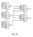
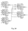
- connection relationship in a circuit such as that shown in Figure 23 is conventionally given as follows. First, unique numbers are assigned to gates, as shown in Figure 24. The input pins of gates are consecutively numbered, starting with 0, from the top.
- connection relationships form a table which provides information on to which gates and to what numbered pin of these gates the output of a certain other gate is to be connected. For example, the output of the tenth gate is connected to the second pin of the thirteenth gate and the second pin of the sixteenth gate.
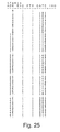
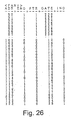
- the method of storing this information in the table will be explained with reference to Figures 25 through 28.
- the first column ADR represents row numbers (addresses) of the table. Thus, the ADR does not represent information to be written into the table.
- the second column to the fifth column represent the actual contents of the table.
- the second column END indicates the end of the list of connection information (the list ends at 1).
- the address 10 of the table is referred to.
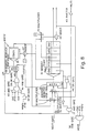
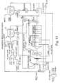
- FIG 29 is a block diagram of hardware for reading numbers of fanout gates from the conventional table with a data structure described in conjunction with Figures 25 through 28.
- This hardware comprises a memory (FAN) 1 for storing the data END, PTR, GATE and INO described in conjunction with Figures 25 to 28, an address register (FADR) 2 for designating an address for reading a fanout gate number from the memory 1, a multiplexer 3 and an OR circuit.
- FAN memory
- FAN memory
- FADR address register
- the compile time is not a serious problem.
- an error (disagreement between the result at a checkpoint of simulation and the expected value) is detected in the simulation machine, the continuation of the simulation is meaningless so long as a design deficiency that causes the error is not removed.
- the occurrence of many errors is inevitable in the initial stage of design in particular.
- the compile time becomes predominant, in which case the logic simulation machine cannot fully show its power.
- a first problem is that, even if the same partial circuit is used in plural locations, this fact is not utilized.
- the circuit of Figure 24 makes repeated use of a partial circuit (macro) of the same structure.
- a circuit comprising gates numbered 10 to 17 and input pins numbered 1 to 3 corresponds to this macro.
- this macro there are four identical macros in the circuit diagram (for example, a circuit comprised of gates 20 to 27 and input pins 4, 5 and 6 and a circuit comprised of gates 40 to 47 and input pins thereto which are shown unnumbered and connected to the output pins of the gates 60, 61 and 62). Such information is not utilized.
- a second problem is that, with the data structure of the conventional table described in conjunction with Figures 25 to 28, addresses corresponding in number to (1 + F) x the number of gates are required, F representing the average number (about three) of fan-outs of a gate.
- F representing the average number (about three) of fan-outs of a gate.
- a third problem which is similar to the second problem, is that the connection information on a certain partial circuit cannot be expanded on a memory to make repeated use of it for other partial circuits of the same structure.
- the invention concerns a gate addressing system according to claim 1.
- the invention also concerns a circuit data expansion system according to claim 6.
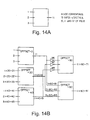
- Figures 1A and 1B are functional block diagrams of first and second principles of the inventions, respectively. These functional block diagrams correspond to a gate addressing system at the time of translation from data in a circuit design data base to circuit data for a logic simulation machine, that is, a gate numbering system.
- the input terminals and gates are numbered in block 10 without using a number corresponding to the number of fanout gates minus one to which an output signal of each input terminal or of each gate is applied. Since, for example, the number of fan-out gates of the input terminal numbered 1 is three in Figure 24, the input terminal numbered 2 in Figure 24 is assigned number 4.
- a table representing connection relationships between an input terminal and a gate and among gates, as described in conjunction with Figures 25 and 28, is configured such that a list of numbers of fanout gates of input terminals and gates starts at addresses as numbers assigned to the input terminals and gates.
- data of address 1 indicates a pointer to a list of the numbers of a fanout gate to which the output signal of the input terminal 1 is applied, as described above.
- the actual list starts at address 101.
- the addresses 2 and 3 can be used for the list.
- the addresses 1 to 3 can be used to represent the list itself.
- Figure 1B which is a functional block diagram of the second principle of the invention, in 12, when there are a plurality of partial circuits having the same arrangement of the input terminal and gates in a circuit, a specific offset value is assigned to each other partial circuit using input terminal and gate numbers of one partial circuit as the reference, and each input terminal and gate is numbered by adding the offset value between corresponding input terminal and between corresponding gate.
- the offset value assigned to each partial circuit is added to the list for the partial circuit used as the reference so that the list of numbers of fanout gates of input terminals and gates may be shared among the plural partial circuits.
- gate numbers which are 10 to 12 and 13 to 17 in Figure 24, are made 4 to 6 and 7 to 11. 1 to 11 correspond to the partial circuit used as the reference.
- input terminals numbered 4 to 6 are assigned 21 to 23 and gates numbered 20 to 27 are assigned numbers 24 to 31, which correspond to the old numbers 10 to 17. That is, the offset value for the second partial circuit relative to the partial circuit used as criterion is 20.
- Figure 2 is a block diagram illustrating the third principle of the present invention, which is directed to a circuit data expansion system in a memory 25 of a logic simulation dedicated machine 24 when a simulation circuit model is generated by compilation of source data.
- a circuit data library 23 stores circuit data resulting from compilation of circuit components to which source data in a source file 21 refers.
- a compile program 22 has the facility to read source data from the source file 21, to take circuit data corresponding to the source data from the circuit data library 23 and to expand it on the memory 25 of the logic simulation dedicated machine 24. It also has the facility to issue a copy instruction to copy the circuit data which is already expanded on the memory 25 onto another location of the memory 25.
- the compile program 22 sequentially reads source data from the source file 21, refers to the circuit data library 23 to take compiled circuit data and expands it on the memory 25.
- the compile program 22 issues a copy instruction to copy this expanded circuit data without taking circuit data from the circuit data library 23 again.
- Figure 3 illustrates a first gate addressing system according to the first principle of the present invention.
- the numbering in the first gate addressing system is characterized in that, first, the relative relationships among gates in macros of the same structure are equal in respective macros and, second, gates are not consecutively numbered.
- the same macro when used in plural locations in a device, it is only required to repeatedly copy the same data into different addresses.
- tables for macros assigned numbers 1 through 20 tables for macros assigned numbers 21 through 40 and tables for three other identical macros have only to store the same contents (thus resolving the first problem).
- each gate is not necessarily required to point to a list and a list can be written below the gate address. Therefore, the number of addresses (1 + F) x the number of gates in the conventional system may be reduced to F x the number of gates (thus resolving the second problem).
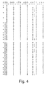
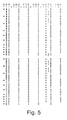
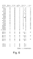
- Figures 4, 5 and 6 illustrate a table of connection relationships corresponding to the first gate addressing system of Figure 4.
- a further column "ADD" is added between columns "PTR" and "GATE".
- ADD 1
- the GATE column is numbered such that the sum of an address number and a number written in the GATE column indicates the actual gate number.
- ADD 0
- the GATE points to a gate number directly as in the conventional system.
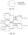
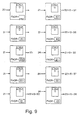
- Figure 7 is a diagram for explaining the macro and hierarchical representation of Figure 3.
- the circuit of Figure 3 is designed hierarchically as shown in Figure 7.
- the macro data shown in Figure A and its connection relationships are described normally.
- the offset values have only to be set so that gate numbers of each macro may not coincide with those of another macro. Since each macro is designed herein to have a size of 19, the offset interval is set to 20. In this way, internal data of the macro can be utilized as it is, thus eliminating the need for renumbering gates.
- the macro need be copied only a few times.
- connections of those having offset values 0, 20 and 40 are defined individually from the addresses 200, 210 and 220 of the table of Figures 4 to 6. This is based on the adoption of an indirect addressing method (pointer). In this way the data structure of Figures 4 to 6 can be generated at a higher speed than with the conventional system.
- connection relationships within a macro are represented by relative values to data storage addresses, thus making data for a plurality of macros basically equal.
- data for addresses 1 to 19 may be equal to those for addresses 21 to 39, 41 to 59, 61 to 79 and 81 to 99.
- the second feature is that the output of the entire macro is expressed by a list pointed to by a pointer. Thus, only one address suffices for one output, the size of a table required for a macro becomes constant regardless of how the output of the macro is connected outside and the address assignment to each macro can be performed independently, at high speed.
- the output gates of the macros are 20, 40 and so on.
- the third feature is that gate addresses are not consecutive and provided including a list of fanout gates, thus reducing the number of pointers. For this reason, the total number of addresses in the system of Figures 4 to 6 is 110, while in the conventional system of Figures 25 to 28 it is 141.
- Figure 8 illustrates an example of connection relationship outputting hardware corresponding to the first gate addressing system.
- 31 denotes a memory (FAN) for storing connection relationship display table data as in the conventional system of Figure 29.
- 32 denotes a register (FADR) for pointing to an address of the table.
- Gates 36 to 44 are control gates.
- 48 is a register which controls an address SADR of the stack.
- the next-gate is loaded into the FADR 32 via the multiplexers 34 and 33.
- a gate number is thereby set in the FADR so that reading of fanout gates from the table 31 is initiated.
- a valid signal from the inverter 43 goes to 1, indicating that effective data are being output to the outside.
- a pointer value is set in the FADR 32 via the multiplexer 33 to read a list pointed to by the pointer. At this point, it is the current FADR value + 1 that is to be returned at the termination of a reading of a preceding list and this value is stored in the stack 35. This is carried out by incrementing the FADR by one and writing FADR + 1 into the stack.
- the pointer data is the last data in the list, it is not stored because its return is not necessary.
- the list When the list is read up to reach its last piece of data, if the last piece of data is a pointer, the next list pointed to by the pointer is read successively. If the last piece of data is not a pointer, the process is returned to the preceding list from which the process is moved. The address of the preceding list is written in the stack. This address is taken into the FADR via the multiplexers 34 and 33 and the SADR value is decremented by one.
- FIG 9 illustrates an example of an operation of the hardware of Figure 10.
- An operation of the hardware in which 20, 21 and 24 are continuously input from outside as next gate numbers is indicated by the contents of the address register (FADR) 32 and stack 35.
- the contents of the stack remain 0.
- END and PTR are both 1s so that no fanout gate number is output and address 81 is stored in the FADR 32 in accordance with pointer value 81.
- the ADD is 1 and the END and PTR are both 0s.
- the address 81 and the contents of the GATE. i.e., +9, are added together and 90 is output as a fanout gate number.
- 97 and 98 are output as fanout gate numbers for addresses 82 and 83.
- the END is 1 so that the fanout gate number list for gate number 20 ends and the next gate number 21 is taken into the FADR 32.
- the fanout gate list for the gate numbered 21 continues up to address 23, in which the END becomes 1 so that fanout gate numbers 37 and 38 for addresses 22 and 23 are read. In this example, a pointer is always placed at the end of a list and thus no data is stored in the stack.
- Figure 10 illustrates another example of the operation of the hardware of Figure 8.
- data except the contents of the END are interchanged between addresses 200 and 201 in the table of Figure 6. That is, in the table of Figure 7, the PTR and GATE in address 200 are changed to 1 and 81, respectively, while the PTR and GATE in address 201 are changed to 0 and 101, respectively.
- the inputting of the next-gate is placed in the wait state when effective data is output to the outside.
- the writing into and reading from the stack are unnecessary and hence it is logically possible to input the next-gate into the stack early.
- the implementation of such hardware is also possible.
- the technique may be applied to generation of a data structure of a simulator serving as software and not as a dedicated machine.
- a data structure of a simulator serving as software and not as a dedicated machine.
- an existing simulator adapted for direct addressing of gates it is necessary in loading circuit data into the simulator to translate relative addresses to direct addresses.
- a non-delay buffer can be inserted into a circuit.
- the buffer is assigned a gate number which can be pointed to by a pointer. This also applies to the case where the compile method is applied to a conventional simulation dedicated machine.
- Figure 11 illustrates a second gate addressing system according to the second principle.
- the feature of gate numbering is that relative relationships among gates in identical macros are equal in respective macros. Gates numbered 1 to 11 and gates numbered 21 to 31 are the same macro. The relative relationship (difference between gate numbers) between corresponding gates is equal for any gate.
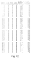
- Figures 12 and 13 illustrates a second connection relationship indicating table corresponding to the second gate addressing system.
- a further column “ADD” is added between columns “PTR” and “GATE”, as for the table of Figures 4 to 6.
- the meaning is the same as that of Figures 4 to 6.
- a fanout gate number contains an offset value of GATE data pointed to by a pointer. If the offset value and ADD are always 0, the second system is the same as the conventional system.
- the use of the addressing system of Figure 11 and the data structure of the table of Figures 12 and 13 eliminates the need to repeatedly copy the same data into different addresses.
- the data has to be held in only one address.
- the pointer offset values permit independent gate numbers to be generated. For example, the pointer of the gate numbered 96 and the pointer in address 201 in the list of the fanout gate numbered 11 both point to 100, but different offset values of 60 and 80 are written in the BASE 2. Offset value 60 points to 64, 68 and 69 in the same macro, while offset value 80 points to 84, 88 and 89 (thus resolving the first problem).
- the table has only to store one type of macro.
- the length of the list can be reduced according to the frequency of repetition of the macro (thus resolving the second problem).
- table address 11 is referred to in order to obtain fanouts of the gate numbered 11.
- the table can express one type of macro using one address, thus reducing the quantity of data (thus resolving the first problem). If a macro is once compiled, its data can be utilized unchanged without the need to renumber gates uniquely as a whole.
- Figure 14 is a diagram for explaining a macro of Figure 11 and hierarchical representation.
- the circuit of Figure 11 is designed hierarchically as illustrated in Figure 14.
- Macro data such as like A and its connection relationship B are normally described.
- An offset value for identifying a macro has only to be set in BASE 2 of a row which points to the macro. Offset values for macros may be set such that their gate numbers do not coincide. Since the size of the macro in this example is 11, the offset interval is set to 20. The offset interval may be 12, but this value makes the correlation of numbers difficult to understand. Thus, 20 is used herein.
- Figure 15 is a block diagram of connection relationship outputting hardware corresponding to the second gate addressing system. Like reference characters are used to designate parts corresponding to those in Figure 8 for the first gate addressing system and their descriptions are omitted.
- the stack (2) 50 of Figure 15 operates in the same manner as the stack 35.
- Data to be stored in the stack 50 is data of BASE 2.
- the contents of a register 51 are 0 and thus the value of BASE 2 is stored in the stack (2) 50 as it is via an adder 52. This corresponds to a first pointer when a list is traced.
- This offset value is stored in the stack (2) 50 and output from the stack (2) at the next clock for addition in an adder 53.
- the value of BASE 2 is added to the current offset value in the adder 52 and then stored in the stack (2).
- the register 51 holds the offset value output from the stack one clock before.
- the stack (2) 50 outputs 0 when no data is stored therein and clears the register 51.
- the stack 50 In the stack 50 are written offset values. At a first-stage pointer the stack (2) is empty so it outputs data 0, making the value in the register 51 0. Thus, data written in BASE 2 becomes an offset value as is. Furthermore, when a pointer is followed, the sum of data written in BASE 2 and the current offset value output from the stack 50 and stored in the register 51 becomes the formal offset value and is stored in the stack 50.
- the address register for the stack (2) is SADR 48, which is also the address register for the stack 35.
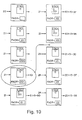
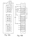
- Figure 16A illustrates an example of three hierarchies. Macros, i.e., partial circuits B0, B1 and B2, are the same as each other.
- the second gate addressing system only data on macro B0 is generated and addresses for macros B1 and B2 are generated on the basis of data on macro B0 by providing an offset BASE 2.
- the offset is set to 100 for macro B1 and to 200 for macro B2. That is, macro B is not more than 100.
- A1 and A2 of the macro B are also the same as each other.
- addresses are generated on the basis of data on A0 by providing each of macros A1 and A2 with an offset BASE 2.
- Figure 16B illustrates addresses which are finally generated in the gate address space.
- a gate number i.e., an address of macro B1
- An address of macro A1 within macro B1 is obtained by adding 100 + 20 to the address of the corresponding gate in macro A0 of macro B0.
- the above-described first pointer corresponds to the case where an inside gate of macro B1 is pointed to from outside, that is, the case where a fanout of a gate external to macro B1 is connected to an inside gate of macro B1.
- the next pointer corresponds to the case where an inside gate of macro A1 is pointed to by a gate external to macro A1.
- the above-described current offset value corresponds, in this case, to 100 and the value of BASE 2 corresponds to 20.
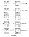
- FIG 17 illustrates an example of operation of the hardware of Figure 15.
- an operation in which 11, 21 and 22 are continuously input from outside as next gate numbers is illustrated with respect to the contents of the address register 32 (FADR) and two stacks 35 and 50.
- FADR address register 32
- FIG. 17 illustrates an example of operation of the hardware of Figure 15.
- an operation in which 11, 21 and 22 are continuously input from outside as next gate numbers is illustrated with respect to the contents of the address register 32 (FADR) and two stacks 35 and 50.
- address 200 is pointed to by the contents in address 11 so that the value of the FADR 32 becomes 200 and gate number 96 is output. At this point the contents of the FADR 32 are incremented to 201. However, address 201 is the end of a list and stores a pointer value so that no fanout gate number is output.
- Address 100 is referred to by the pointer value in address 201.
- the offset value 80 in address 201 is stored in the second stack 50.
- 84 is output as a fanout gate number.
- fanout gate numbers 88 and 89 are output until address 102 is reached.
- the outputting of fanout gate numbers for the gate 11 terminates.
- the next gate number 21 is read into the FADR 32.
- the data in address 21 is a pointer value 100 and an offset value is 20.
- the FADR 32 becomes 100 and the second stack 50 becomes 20 so that a fanout gate number 24 for address 100 is output and fanout gate numbers for addresses succeeding address 100 continue to be output.
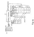
- a source file 21 stores source data which describes the structure of a circuit to be simulated.
- the source file 21 contains connection relationships among pins of the circuit (circuit components), etc.
- a compile program 22 reads source data from the source file 21 in sequence, takes relevant circuit data from a circuit data library 23 for translation from a relative address to an absolute address and expansion on a memory 25, transfers relevant circuit data from the circuit data library 23 directly to a simulation dedicated machine 24 with a relative address, expands the data on the memory 25 after translation to an absolute address (when a relative address to absolute address translation facility is installed), and issues a copy instruction to copy circuit data expanded on the memory 25.
- the circuit data library 23 previously stores circuit data resulting from compilation of circuit components to which source data refers. This circuit data library 23 stores in advance compiled circuit data, memory capacity for circuit data and so on.
- the logic simulation dedicated machine 24 is adapted for high-speed logic simulation (computer system).
- the memory 25 is installed in the logic simulation dedicated machine 24 and adapted to expand circuit data for simulation execution.
- the source file 21 stores source data for two components a, one component b, three components c, one component d and three components e.
- the circuit data library 23 stores circuit data a, circuit data b, circuit data c, circuit data d and circuit data e resulting from compilation of component a, component b, component c, component d and component e, and memory sizes for those circuit data (a. memory size is expressed by the size of a rectangle).
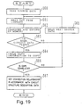
- source data are read in step S60. That is, source data (for example, a x 2) are read from the source file 21 on a row-by-row basis.
- relevant data for example, circuit data a
- circuit data library 23 relevant data
- the relevant circuit data are transferred and expanded on the memory. That is, the compile program 22 issues a circuit data transfer instruction so as to transfer circuit data (for example, circuit data a) from circuit data library 23 to the logic simulation dedicated machine memory 25, as indicated by an arrow in Figure 18, and expands it on the memory.
- circuit data for example, circuit data a
- S63 a determination is made as to whether or not the same data is plural. If YES (for example, when the first source data a x 2 is read from the source file 21), the process of S64 is performed. If NO, next data are read in S65 and the process returns to S61.
- step S64 a copy instruction is issued to copy circuit data. That is, since it has been determined in step S63 that the same data is plural, the circuit data (for example, circuit data a) expanded on the logic simulation dedicated machine memory 25 is copied by the relevant number.
- S66 a determination is made as to whether or not the compilation has been terminated, that is, whether or not all pieces of source data have been read. If YES, the connection relationships of the circuit data expanded on the logic simulation dedicated machine memory 25 are set in accordance with the circuit structure descriptive data in the source file 21 and then stored in a suitable location in S67. If NO, the next data are read in S65 and the process returns to S61.
- circuit data relevant to the source data read from the source file 21 are read from the circuit data library 23 and expanded on the logic simulation dedicated machine memory 25, as shown in Figure 18. By copying the same data, it expands the compiled circuit data on the logic simulation dedicated machine memory 25 with a small amount of data from the source file 21.
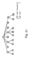
- Figure 20A illustrates an example of circuit components. This is a schematic representation of circuit structures described in the source file 21.
- the component 1 is constructed from two components 2, one component 3, one component 4, one component 5 and three components 6.
- the component 2 is comprised of two components 4; the component 3 is comprised of one component 7 and one component 4; the component 5 is comprised of one component 4, one component 8 and one component 9; and the component 6 is comprised of one component 9 and one component 10.
- Figure 20B illustrates the hierarchical structures of the various components of Figure 20A.
- Figure 20C illustrates the combined hierarchical structure of Figure 20B.
- Figure 21 illustrates an example of the order of data transfer/copy.
- ⁇ indicates a component whose data is transferred from the circuit data library 23 to the logic simulation dedicated machine memory 25 and expanded thereon, while “ ⁇ ” indicates a component to be copied on the logic simulation dedicated machine memory 25. This is described hereinafter.
- Figure 22 is a flowchart of the simulation executing process.
- circuit data are fetched from the logic simulation dedicated machine memory 25 in S71.
- an event is waited to fetch the next circuit data.
- a concrete example of the event here is such that a signal at the output pin of a gate A has gone to 1.
- the simulator fetches the destination to which the output pin of the gate A to be connected from the circuit data, updates a signal value of an input pin of the destination gate, and evaluates and updates a signal value of the output pin of the gate.
Landscapes
- Engineering & Computer Science (AREA)
- Computer Hardware Design (AREA)
- Physics & Mathematics (AREA)
- Theoretical Computer Science (AREA)
- Evolutionary Computation (AREA)
- Geometry (AREA)
- General Engineering & Computer Science (AREA)
- General Physics & Mathematics (AREA)
- Test And Diagnosis Of Digital Computers (AREA)
Priority Applications (2)
| Application Number | Priority Date | Filing Date | Title |
|---|---|---|---|
| EP01200829A EP1187043A2 (en) | 1990-01-29 | 1991-01-29 | Gate addressing system for logic simulation machine |
| EP01200828A EP1115072A2 (en) | 1990-01-29 | 1991-01-29 | Gate addressing system for logic simulation machine |
Applications Claiming Priority (6)
| Application Number | Priority Date | Filing Date | Title |
|---|---|---|---|
| JP18420/90 | 1990-01-29 | ||
| JP1842090 | 1990-01-29 | ||
| JP1842090 | 1990-01-29 | ||
| JP21782990 | 1990-08-18 | ||
| JP21782990 | 1990-08-18 | ||
| JP217829/90 | 1990-08-18 |
Related Child Applications (2)
| Application Number | Title | Priority Date | Filing Date |
|---|---|---|---|
| EP01200828A Division EP1115072A2 (en) | 1990-01-29 | 1991-01-29 | Gate addressing system for logic simulation machine |
| EP01200829A Division EP1187043A2 (en) | 1990-01-29 | 1991-01-29 | Gate addressing system for logic simulation machine |
Publications (3)
| Publication Number | Publication Date |
|---|---|
| EP0440553A2 EP0440553A2 (en) | 1991-08-07 |
| EP0440553A3 EP0440553A3 (cg-RX-API-DMAC10.html) | 1994-02-16 |
| EP0440553B1 true EP0440553B1 (en) | 2001-10-17 |
Family
ID=26355092
Family Applications (3)
| Application Number | Title | Priority Date | Filing Date |
|---|---|---|---|
| EP91400213A Expired - Lifetime EP0440553B1 (en) | 1990-01-29 | 1991-01-29 | Gate addressing system for logic simulation machine |
| EP01200829A Withdrawn EP1187043A2 (en) | 1990-01-29 | 1991-01-29 | Gate addressing system for logic simulation machine |
| EP01200828A Withdrawn EP1115072A2 (en) | 1990-01-29 | 1991-01-29 | Gate addressing system for logic simulation machine |
Family Applications After (2)
| Application Number | Title | Priority Date | Filing Date |
|---|---|---|---|
| EP01200829A Withdrawn EP1187043A2 (en) | 1990-01-29 | 1991-01-29 | Gate addressing system for logic simulation machine |
| EP01200828A Withdrawn EP1115072A2 (en) | 1990-01-29 | 1991-01-29 | Gate addressing system for logic simulation machine |
Country Status (3)
| Country | Link |
|---|---|
| US (1) | US5245549A (cg-RX-API-DMAC10.html) |
| EP (3) | EP0440553B1 (cg-RX-API-DMAC10.html) |
| DE (1) | DE69132766T2 (cg-RX-API-DMAC10.html) |
Families Citing this family (4)
| Publication number | Priority date | Publication date | Assignee | Title |
|---|---|---|---|---|
| US5500808A (en) * | 1991-01-24 | 1996-03-19 | Synopsys, Inc. | Apparatus and method for estimating time delays using unmapped combinational logic networks |
| US5978571A (en) * | 1993-03-19 | 1999-11-02 | Digital Equipment Corporation | Method and apparatus for synchronous circuit simulation design by eliminating unneeded timing behaviors prior to simulation run-time |
| US5648911A (en) * | 1993-12-21 | 1997-07-15 | Grodstein; Joel Joseph | Method of minimizing area for fanout chains in high-speed networks |
| US10776543B2 (en) | 2018-06-25 | 2020-09-15 | International Business Machines Corporation | Automated region based optimization of chip manufacture |
Family Cites Families (8)
| Publication number | Priority date | Publication date | Assignee | Title |
|---|---|---|---|---|
| JPS593652A (ja) * | 1982-06-30 | 1984-01-10 | Fujitsu Ltd | ハ−ド論理シミユレ−タ装置 |
| JPS5975347A (ja) * | 1982-10-21 | 1984-04-28 | Toshiba Corp | 論理回路のシミユレ−シヨン装置 |
| JPH0743733B2 (ja) * | 1985-12-11 | 1995-05-15 | 株式会社日立製作所 | 論理シミュレーション方法 |
| JPS6381567A (ja) * | 1986-09-26 | 1988-04-12 | Hitachi Ltd | 論理シミユレ−シヨン処理装置 |
| JPS63204441A (ja) * | 1987-02-20 | 1988-08-24 | Fujitsu Ltd | 論理シミユレ−シヨン専用プロセツサの処理方式 |
| JP2699377B2 (ja) * | 1987-02-25 | 1998-01-19 | 日本電気株式会社 | ハードウエア論理シミユレータ |
| US4816999A (en) * | 1987-05-20 | 1989-03-28 | International Business Machines Corporation | Method of detecting constants and removing redundant connections in a logic network |
| US5051938A (en) * | 1989-06-23 | 1991-09-24 | Hyduke Stanley M | Simulation of selected logic circuit designs |
-
1991
- 1991-01-29 EP EP91400213A patent/EP0440553B1/en not_active Expired - Lifetime
- 1991-01-29 EP EP01200829A patent/EP1187043A2/en not_active Withdrawn
- 1991-01-29 EP EP01200828A patent/EP1115072A2/en not_active Withdrawn
- 1991-01-29 DE DE69132766T patent/DE69132766T2/de not_active Expired - Fee Related
- 1991-01-29 US US07/647,704 patent/US5245549A/en not_active Expired - Fee Related
Also Published As
| Publication number | Publication date |
|---|---|
| EP1187043A2 (en) | 2002-03-13 |
| EP1115072A2 (en) | 2001-07-11 |
| DE69132766T2 (de) | 2002-04-25 |
| EP0440553A3 (cg-RX-API-DMAC10.html) | 1994-02-16 |
| US5245549A (en) | 1993-09-14 |
| EP0440553A2 (en) | 1991-08-07 |
| DE69132766D1 (de) | 2001-11-22 |
Similar Documents
| Publication | Publication Date | Title |
|---|---|---|
| US6370677B1 (en) | Method and system for maintaining hierarchy throughout the integrated circuit design process | |
| JP2989518B2 (ja) | 多重プロセッサ・エミュレーション・システム | |
| US5937179A (en) | Integrated circuit design system with shared hardware accelerator and processes of designing integrated circuits | |
| EP0433066A2 (en) | Common symbol library architecture | |
| US5548785A (en) | Interface for logic simulation using parallel bus for concurrent transfers and having fifo buffers for sending data to receiving units when ready | |
| US4584642A (en) | Logic simulation apparatus | |
| Gustafson et al. | IBM 3081 processor unit: Design considerations and design process | |
| EP0440553B1 (en) | Gate addressing system for logic simulation machine | |
| US5774380A (en) | State capture/reuse for verilog simulation of high gate count ASIC | |
| Szygenda et al. | Integrated techniques for functional and gate-level digital logic simulation | |
| JPH03209569A (ja) | 論理シミュレーション方法 | |
| US12112818B2 (en) | Scan chain compression for testing memory of a system on a chip | |
| JP3667146B2 (ja) | メモリ用内蔵自己テスト回路 | |
| EP1031995B1 (en) | Built-in self-test circuit for memory | |
| US6189129B1 (en) | Figure operation of layout for high speed processing | |
| JPH04211870A (ja) | 論理シミュレーションマシンのゲートアドレッシング方式 | |
| Navabi et al. | Templates for synthesis from VHDL | |
| Martinez et al. | Compilation of standard-cell libraries | |
| JP2648528B2 (ja) | Lsi設計方法 | |
| JP2692813B2 (ja) | スキャン化回路変換方法 | |
| JP3696302B2 (ja) | テストベクトル生成方法及び生成装置 | |
| JP2990882B2 (ja) | 機能シミュレーション装置 | |
| CN115586425A (zh) | 用于测试片上系统的存储器的扫描链压缩 | |
| Gebotys et al. | Global VLSI Design Cycle | |
| Hur et al. | Massively parallel array processor for logic, fault, and design error simulation |
Legal Events
| Date | Code | Title | Description |
|---|---|---|---|
| PUAI | Public reference made under article 153(3) epc to a published international application that has entered the european phase |
Free format text: ORIGINAL CODE: 0009012 |
|
| AK | Designated contracting states |
Kind code of ref document: A2 Designated state(s): DE FR GB |
|
| PUAL | Search report despatched |
Free format text: ORIGINAL CODE: 0009013 |
|
| AK | Designated contracting states |
Kind code of ref document: A3 Designated state(s): DE FR GB |
|
| 17P | Request for examination filed |
Effective date: 19940411 |
|
| 17Q | First examination report despatched |
Effective date: 19980429 |
|
| RIC1 | Information provided on ipc code assigned before grant |
Free format text: 7G 06F 17/50 A |
|
| GRAG | Despatch of communication of intention to grant |
Free format text: ORIGINAL CODE: EPIDOS AGRA |
|
| GRAG | Despatch of communication of intention to grant |
Free format text: ORIGINAL CODE: EPIDOS AGRA |
|
| GRAH | Despatch of communication of intention to grant a patent |
Free format text: ORIGINAL CODE: EPIDOS IGRA |
|
| GRAH | Despatch of communication of intention to grant a patent |
Free format text: ORIGINAL CODE: EPIDOS IGRA |
|
| GRAA | (expected) grant |
Free format text: ORIGINAL CODE: 0009210 |
|
| AK | Designated contracting states |
Kind code of ref document: B1 Designated state(s): DE FR GB |
|
| REF | Corresponds to: |
Ref document number: 69132766 Country of ref document: DE Date of ref document: 20011122 |
|
| REG | Reference to a national code |
Ref country code: GB Ref legal event code: IF02 |
|
| ET | Fr: translation filed | ||
| ET1 | Fr: translation filed ** revision of the translation of the patent or the claims | ||
| PLBE | No opposition filed within time limit |
Free format text: ORIGINAL CODE: 0009261 |
|
| STAA | Information on the status of an ep patent application or granted ep patent |
Free format text: STATUS: NO OPPOSITION FILED WITHIN TIME LIMIT |
|
| 26N | No opposition filed | ||
| PGFP | Annual fee paid to national office [announced via postgrant information from national office to epo] |
Ref country code: FR Payment date: 20040108 Year of fee payment: 14 |
|
| PGFP | Annual fee paid to national office [announced via postgrant information from national office to epo] |
Ref country code: GB Payment date: 20040128 Year of fee payment: 14 |
|
| PGFP | Annual fee paid to national office [announced via postgrant information from national office to epo] |
Ref country code: DE Payment date: 20040205 Year of fee payment: 14 |
|
| PG25 | Lapsed in a contracting state [announced via postgrant information from national office to epo] |
Ref country code: GB Free format text: LAPSE BECAUSE OF NON-PAYMENT OF DUE FEES Effective date: 20050129 |
|
| PG25 | Lapsed in a contracting state [announced via postgrant information from national office to epo] |
Ref country code: DE Free format text: LAPSE BECAUSE OF NON-PAYMENT OF DUE FEES Effective date: 20050802 |
|
| GBPC | Gb: european patent ceased through non-payment of renewal fee |
Effective date: 20050129 |
|
| PG25 | Lapsed in a contracting state [announced via postgrant information from national office to epo] |
Ref country code: FR Free format text: LAPSE BECAUSE OF NON-PAYMENT OF DUE FEES Effective date: 20050930 |
|
| REG | Reference to a national code |
Ref country code: FR Ref legal event code: ST |