EP0439939B1 - Funknetzwerk mit Schalteinrichtung zum Koppeln von Funkgeräten an eine ausgewählte Antenne aus einer Vielzahl von Antennen - Google Patents
Funknetzwerk mit Schalteinrichtung zum Koppeln von Funkgeräten an eine ausgewählte Antenne aus einer Vielzahl von Antennen Download PDFInfo
- Publication number
- EP0439939B1 EP0439939B1 EP90313757A EP90313757A EP0439939B1 EP 0439939 B1 EP0439939 B1 EP 0439939B1 EP 90313757 A EP90313757 A EP 90313757A EP 90313757 A EP90313757 A EP 90313757A EP 0439939 B1 EP0439939 B1 EP 0439939B1
- Authority
- EP
- European Patent Office
- Prior art keywords
- antennas
- switch
- signal
- radio
- arrangement
- Prior art date
- Legal status (The legal status is an assumption and is not a legal conclusion. Google has not performed a legal analysis and makes no representation as to the accuracy of the status listed.)
- Expired - Lifetime
Links
Images


Classifications
-
- H—ELECTRICITY
- H01—ELECTRIC ELEMENTS
- H01Q—ANTENNAS, i.e. RADIO AERIALS
- H01Q3/00—Arrangements for changing or varying the orientation or the shape of the directional pattern of the waves radiated from an antenna or antenna system
- H01Q3/24—Arrangements for changing or varying the orientation or the shape of the directional pattern of the waves radiated from an antenna or antenna system varying the orientation by switching energy from one active radiating element to another, e.g. for beam switching
Definitions
- This invention relates to switched radio antenna interconnection arrangements.
- Cell sites in a cellular radio telephone system include antenna arrays to provide radio service to the total area of the site. These arrays normally include an omni-directional antenna and a plurality of directional antennas arranged for signal transmission in defined sectors or angular sweeps of the cell area and two omnidirectional antennas and a plurality of directional antennas arranged for reception of mobile transmissions from defined sectors or angular sweeps of the cell area.
- the number of radios connected to each directional antenna reflects the radio traffic in each sector. Since the connections are made manually by a craftsman, the number of radios dedicated to a particular sector cannot be readily changed to meet dynamically changing use patterns. Hence some sector facilities may be over burdened while other sectors are underutilized.
- US Patent 4,233,310 discloses an antenna system permitting an antenna array to be individually connected to a receiver and to one of a plurality of transmitters.
- Antenna coupler means are provided to connect each of the antennas to a selected transmitter and a separate receiver.
- Signal isolation is provided between the transmitter input and receiver output terminals so that an antenna coupler may connect a single antenna to a separate transmitter and receiver.
- the receiving antennas of a cellular telephone system are each connected to a unique antenna connecting path.
- Each antenna connecting path is connected to a signal divider which divides the antenna connecting path into a plurality of radio channel unit connecting paths.
- One radio channel unit connecting path from each of the plurality of signal dividers is connected to a controllable switch which in turn selectively couples a radio channel unit connecting path to a transceiver.
- each transceiver For the transmission of signals from base station radio transceivers, the output of each transceiver is connected to a unique controllable switch which in turn selectively couples the transceiver output to any one of a plurality of signal combiners.
- Each of the signal combiners combines the radio channel unit transmit path with a plurality of other channel unit transmit paths into one antenna connecting path.
- Each antenna connecting path is associated with a unique transmitting antenna.
- the antenna transmission/receive paths comprising the signal divider/combiners are embodied as strip type transmission lines in a multi layer PCB with all the paths having equal signal transmission loss.
- Micro vias are provided to permit electrical access to the various layers.
- the controllable switches are surface mounted on the outside of the PCB and are coupled to the various dividers through the micro vias. Remote control of the switches permits a radio channel unit transceiver to be connected to any one of the array of antennas.
- FIG. 1 A block schematic of a transmission path connecting a plurality of radio channel unit transmitters 101 to a plurality of antennas 111 is shown in FIG. 1.
- Each radio channel unit transmitter 101 is connected via individual circuit paths 102 to a selector switch and signal combiner 103 which places all the incoming individual signals from transmission paths 102 on one of a plurality of output transmission paths 104. From there the output of the selected transmission path may be further combined in the transmission process, however these functions are not disclosed in order to simplify the illustrative system.
- the signals on the selected output transmission path 104 are applied to a combining and amplification circuitry 105 which includes a highly linear amplifier and which is capable of handling a plurality of message signals with a minimum of distortion.
- the output of this amplifier circuitry 105 is applied in this particular selected circuit path, via a filter 107 to a selected one of a plurality of transmitting antennas 111.
- a reception path coupling a selected one of a plurality of receiving antennas 211 to a plurality of radio channel unit receivers 201 is shown in block schematic form in FIG. 2.
- the received signal is transmitted, via a filter 207, and a pre amplifier 205 to a signal divider and selector switch 203 which splits the received signal to a the plurality of receiving paths 202 each coupled in turn to a radio channel unit receiver 201.
- FIG. 3 A schematic of the generalized switch divider/combiner topology applicable to both transmission and reception paths is schematically disclosed in FIG. 3.
- An illustrative cell site antenna array having three directional antennas 301,302 and 303 and an omni-directional antenna 304. Each antenna is coupled (although not necessarily directly connected) to a signal divider/combiner 311-314.
- Each signal divider/combiner in the illustrative embodiment divides by a 1:12 ratio (reception) or combines a signal in a 12:1 ratio (transmission) by transforming a circuit path having one lead at one terminal end having one lead 331 to twelve leads 333 at the other terminal end of the switch.
- Each conducting path traverse through the signal combiner/divider has a substantially identical overall path impedance so that a signal will be accurately divided or combined with a uniform attenuation.
- These identical overall path impedances are achieved by making path lengths substantially identical where ever possible and by inserting signal attenuation means within selected paths where needed to compensate for path traverse length differences. An illustrative example is discussed below with reference to FIG. 5.
- Each one of the twelve leads of terminal end 333 of each signal divider/combiner 311 - 314 is connected to one of twelve single pole four throw switch (there is one throw connection for coupling to each individual antenna) which in turn connects each one of these leads to a particular radio channel unit.
- twelve four throw switches 351-362 connected to twelve radio channel units 371 - 382, respectively, however, it is to be understood that may other combinations are within the scope of the invention.
- this arrangement permits each of the twelve radio channel units 371-382 to be connected to any one of the four antennas 301 - 304.
- message signals would originate in a radio transmitter in the radio channel unit 371 for example.
- the transmitted signal would be coupled to the single pole-four throw switch 351. Its particular pole throw connection determines which of the signal divider/combiners it is connected to. With the pole throw connector illustrated, the transmitted signal is connected to the left most lead of signal divider/combiner 311. It is transmitted to the lead 331 and from there to antenna 301.
- the in-coming message signal received by antenna 301 would be applied to lead 331 and by the signal splitting action of signal divider/combiner 311 appears at all twelve of its terminal leads 333. In this illustrative embodiment, it would be coupled by the single pole four throw switch 351 to a radio receiver at radio channel unit 371. It is to be understood that the schematically shown apparatus of FIG. 3 is not a single circuit with transmitting and receiving modes. Transmission and reception requires different circuits due to the differing signal amplification and signal isolation requirements.
- FIG. 4 This particular arrangement is shown in generalized block schematic form in FIG. 4 where the four antennas designated $alpha$, $beta$, $gamma$ and omni are coupled to the connecting leads 401-404.
- These connecting leads 401-404 are connected, via the amplifiers 411-414 in a receiving version of the circuitry, to four switch divider/combiners designated as the block 421. In a transmission version of the circuitry these amplifiers 411-414 are either oppositely directed or not needed.
- These four signal divider/combiners in block 421 are coupled to the twelve single pole four throw switches 451-462 in the manner indicated in FIG. 3.
- Each of the signal pole four throw switches in the illustrative embodiment is an electronically controllable semiconductor switch arrangement.
- the switches 451 - 462 utilize gallium-arsenide FET switches in a logical circuit where the pole-throw connection is responsive to an applied input switch control code.
- a requirement of the switch, particularly for transmission arrangements, is the provision of a high degree of electrical isolation between the poles and the individual throw contacts. A value of 45 dB of isolation between pole and throw contact is provided in the illustrative embodiment.
- Each of the switches 451 - 462 includes a control input designated by switch control inputs 471 - 482.
- a code applied to this input determines the pole-throw connection of the switch. In the illustrative embodiment this is a two bit code applied on a two lead input as indicated by the "2" designation.
- This code is provided by a switch control circuit 490 which is illustratively functionally shown as having twelve independent two lead outputs 492 that are coupled to the twelve switch control inputs 471 - 482, respectively.
- This switch control 490 may be practically embodied by having switch control logic circuitry being resident on individual radio channel units. Each radio channel unit in this arrangement has twelve independent two lead outputs which are coupled to the twelve switch control inputs 471-482.
- Switch control 490 is shown as being functionally responsive to a control input 498. Such a control input may be manually applied or it may be accomplished by an automatic control entity which analyzes cellular phone traffic and selects radio channel unit - antenna connections to optimize the utilization of system resources.
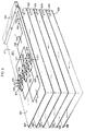
- the signal divider/combiners and the pole-throw switches are all embodied in a single integrated circuit package as shown in FIG. 5.
- This circuit package comprises a plurality of substrates 501 through 506 which are layered and bonded together to form a multi layer circuit package which comprises circuitry formed on the twelve layers in the illustrative embodiment shown in FIG. 5. Each individual layer has a specific circuit pattern to perform a specific function.
- the signal transmission paths for two of the signal divider/combiner arrays are deposited to form the array of strip type transmission lines 551 on the top layer 511 of substrate 501. These particular transmission lines, sometimes designated as flat strip conductors, are formed with a strip conductor deposited above a single ground plane. This ground plane is formed on the bottom layer 521 of the substrate 501.
- Layer 512 of substrate 502 contains DC power distribution circuitry, switch logic distribution circuitry and a ground plane.
- Layer 522 of substrate 502 contains DC power distribution circuitry and a ground plane.
- Layer 513 of substrate 503 contains a ground plane while layer 523 contains strip type transmission circuitry ground plane.
- Layer 514 and 524 of substrate 504 contains signal input/output strip type transmission circuitry and a ground plane.
- Layer 514 also contains DC power distribution circuitry.
- Layer 515 of substrate 505 contains signal input/output strip type transmission circuitry and a ground plane while layer 525 contains a ground plane.
- Layer 516 of substrate 506 contains ground plane. The remaining two signal combiner/divider arrays similar to layer 511 utilizing strip type transmission lines are deposited on the bottom layer 526 of substrate 506.
- a typical layout of the strip type transmission lines 551 forming the switch divider/combiner circuit paths is illustratively shown for the top surface 511 of the substrate 501.
- Two surface terminals 552 and 553 are connected to a connecting block, having coaxial receptacles for rf signals, which enables the coupling of circuits within the switch package to an rf backplane of a circuit support frame.
- the terminals 552 and 553 are connected, via the strip like transmission paths 532 and 533, to the two 12:1 divider/combiner arrays 542 and 543, respectively.
- the attenuators 534 and 535 are included in the paths 532 and 533 to compensate for the differences in path length of transmission paths 532 and 533 by equalizing the overall transmission path loss.
- Two signal divider/combiner arrays and six single pole four throw switches are included on the bottom layer 526. These arrays are also connected to the connector block and in addition include attenuators for equalizing transmission path losses.
- Switches 544 - 549 are surface mounted on the top and bottom layers 511 and 526 respectively in the illustrative embodiment. Connections to the inner signal divider/combiner arrays are by micro-vias (holes in the substrate with conductive plating). The other six multiple terminal ends of each of the two 12:1 signal divider/combiner arrays on the top layer 511 are connected to the six single-pole-four throw switches on bottom layer 526 via the micro-vias 571.
Landscapes
- Variable-Direction Aerials And Aerial Arrays (AREA)
- Mobile Radio Communication Systems (AREA)
Claims (4)
- Geschaltete Funkantennen-Verbindungseinrichtung mit einer Vielzahl von Antennen (301 bis 304),
eine Vielzahl von Funksendeempfängern (371 bis 382) zur Aussendung und zum Empfang von Funktionsignalen über gewählte Antennen aus der Vielzahl von Antennen und einer Verbindungseinrichtung zur Ermöglichung geschalteter Verbindungen zwischen der Vielzahl von Funksendeempfängern und der Vielzahl von Antennen, gekennzeichnet durch
eine Vielzahl von Verzweigungsstromweganordnungen (311, 312, 313, 314), die je Einzelleitungs-zu-Vielfachleitungsverbindungen ermöglichen,
wobei jedes Vielfachleitungsende jeder Anordnung mit einem Koppler (351 bis 362) verbunden ist und jeder Koppler eine Verbindung zu einem entsprechenden Funksendeempfänger der Vielzahl von Funksendeempfänger (371 bis 382) ermöglicht,
jede Einzelleitungsseite jeder Anordnung mit einer entsprechenden Antenne der Vielzahl von Antennen (301 bis 304) verbunden ist und
eine Steuerschaltung, die die Verbindung eines Funksendeempfängers mit einem bestimmten Ende der Vielfachleitungsenden steuert. - Einrichtung nach Anspruch 1,
bei der jede Anordnung Streifenübertragungsleitungen auf einem Substrat enthält, die Leitungen eine Baumtopologie zwischen der Einzelleitungsseite und den Vielfachleitungsenden besitzen, und jeder Koppler eine Verbindung von einem einzelnen zu mehreren Polen besitzt und auf dem Substrat befestigt ist. - Einrichtung nach Anspruch 2,
bei der die Anordnungen auf einer Vielzahl von Substratschichten angeordnet sind. - Einrichtung nach Anspruch 3,
bei der jede Anordnung eine Signalabschwächung zur Erzielung einer einheitlichen Dämpfung zwischen der Einzel-auf-Vielfachleitungsverbindung aufweist.
Applications Claiming Priority (2)
| Application Number | Priority Date | Filing Date | Title |
|---|---|---|---|
| US474562 | 1990-02-02 | ||
| US07/474,562 US5175878A (en) | 1990-02-02 | 1990-02-02 | Radio network with switching arrangement for coupling radios to a selected antenna out of a plurality of antennas |
Publications (3)
| Publication Number | Publication Date |
|---|---|
| EP0439939A2 EP0439939A2 (de) | 1991-08-07 |
| EP0439939A3 EP0439939A3 (en) | 1992-03-04 |
| EP0439939B1 true EP0439939B1 (de) | 1995-09-20 |
Family
ID=23884080
Family Applications (1)
| Application Number | Title | Priority Date | Filing Date |
|---|---|---|---|
| EP90313757A Expired - Lifetime EP0439939B1 (de) | 1990-02-02 | 1990-12-17 | Funknetzwerk mit Schalteinrichtung zum Koppeln von Funkgeräten an eine ausgewählte Antenne aus einer Vielzahl von Antennen |
Country Status (4)
| Country | Link |
|---|---|
| US (1) | US5175878A (de) |
| EP (1) | EP0439939B1 (de) |
| JP (1) | JPH04347937A (de) |
| DE (1) | DE69022572T2 (de) |
Cited By (1)
| Publication number | Priority date | Publication date | Assignee | Title |
|---|---|---|---|---|
| WO2009143293A3 (en) * | 2008-05-20 | 2010-08-05 | Finisar Corporation | Transceiver module with dual printed circuit boards |
Families Citing this family (53)
| Publication number | Priority date | Publication date | Assignee | Title |
|---|---|---|---|---|
| US5708833A (en) | 1993-04-27 | 1998-01-13 | Norand Corporation | Antenna cap, antenna connectors and telephone line connectors for computer devices utilizing radio and modem cards |
| US5021801A (en) * | 1989-09-05 | 1991-06-04 | Motorola, Inc. | Antenna switching system |
| JP2778293B2 (ja) * | 1991-07-04 | 1998-07-23 | ソニー株式会社 | 衛星放送受信システム及び切換分配器 |
| SE470078B (sv) * | 1992-03-27 | 1993-11-01 | Ericsson Telefon Ab L M | Basstation för cellindelade frekvenshoppande TDMA- radiokommunikationssystem |
| SE470520B (sv) * | 1992-11-09 | 1994-06-27 | Ericsson Telefon Ab L M | Radiomodul ingående i en primär radiostation jämte radiostruktur innehållande sådana moduler |
| US5488737A (en) * | 1992-11-17 | 1996-01-30 | Southwestern Bell Technology Resources, Inc. | Land-based wireless communications system having a scanned directional antenna |
| US5991864A (en) * | 1993-04-27 | 1999-11-23 | Intermec Ip Corp. | Power connectors, antenna connectors and telephone line connectors for computer devices utilizing radio and modem cards |
| US7119750B2 (en) * | 1993-04-27 | 2006-10-10 | Broadcom Corporation | Radio transceiver card communicating in a plurality of frequency bands |
| DE4322863C2 (de) * | 1993-07-09 | 1995-05-18 | Ant Nachrichtentech | Mobilfunkantennenanlage |
| GB2281012B (en) * | 1993-08-12 | 1998-04-15 | Northern Telecom Ltd | Angle diversity for multiple beam antenna |
| US6157668A (en) * | 1993-10-28 | 2000-12-05 | Qualcomm Inc. | Method and apparatus for reducing the average transmit power of a base station |
| ZA948134B (en) * | 1993-10-28 | 1995-06-13 | Quaqlcomm Inc | Method and apparatus for performing handoff between sectors of a common base station |
| ZA948133B (en) * | 1993-10-28 | 1996-05-17 | Qualcomm Inc | Method and apparatus for reducing the average transmit power from a sectorized base station |
| US5771449A (en) * | 1994-03-17 | 1998-06-23 | Endlink, Inc. | Sectorized multi-function communication system |
| US5793762A (en) * | 1994-04-12 | 1998-08-11 | U S West Technologies, Inc. | System and method for providing packet data and voice services to mobile subscribers |
| US5457736A (en) * | 1994-04-12 | 1995-10-10 | U S West Technologies, Inc. | System and method for providing microcellular personal communications services (PCS) utilizing embedded switches |
| US5818385A (en) * | 1994-06-10 | 1998-10-06 | Bartholomew; Darin E. | Antenna system and method |
| TW280064B (de) * | 1994-09-29 | 1996-07-01 | Radio Frequency Systems Inc | |
| US5701596A (en) * | 1994-12-01 | 1997-12-23 | Radio Frequency Systems, Inc. | Modular interconnect matrix for matrix connection of a plurality of antennas with a plurality of radio channel units |
| KR960027576A (ko) * | 1994-12-01 | 1996-07-22 | 리차드 탤런 | 육상 이동 무선 베이스 사이트에 사용되는 무선 신호 스캐닝 및 타겟팅 시스템 |
| US5579341A (en) * | 1994-12-29 | 1996-11-26 | Motorola, Inc. | Multi-channel digital transceiver and method |
| US5684491A (en) * | 1995-01-27 | 1997-11-04 | Hazeltine Corporation | High gain antenna systems for cellular use |
| US5933787A (en) * | 1995-03-13 | 1999-08-03 | Qualcomm Incorporated | Method and apparatus for performing handoff between sectors of a common base station |
| US5854986A (en) * | 1995-05-19 | 1998-12-29 | Northern Telecom Limited | Cellular communication system having device coupling distribution of antennas to plurality of transceivers |
| RU2141723C1 (ru) * | 1995-06-16 | 1999-11-20 | Калининградское высшее военно-морское училище | Радиостанция |
| US5608724A (en) * | 1995-09-27 | 1997-03-04 | Nippondenso Co., Ltd. | Dynamically reconfigurable frequency division multiplexer and modulator |
| US5815116A (en) * | 1995-11-29 | 1998-09-29 | Trw Inc. | Personal beam cellular communication system |
| US5669060A (en) * | 1996-03-04 | 1997-09-16 | Telefonaktiebolaget L M Ericsson (Publ) | Method and apparatus for enhancing call set-up and handoff quality |
| JP3076252B2 (ja) * | 1996-11-25 | 2000-08-14 | 日本電気株式会社 | セルラー移動通信システムにおける多セクター切替制御装置 |
| KR100202502B1 (ko) * | 1996-12-30 | 1999-06-15 | 정장호 | 이동통신시스템 기지국의 시험회로 |
| US5913177A (en) * | 1997-03-31 | 1999-06-15 | Radio Frequency Systems, Inc. | Traffic distribution analysis in a land mobile radio system |
| CA2356879A1 (en) * | 1998-12-23 | 2000-07-06 | Telefonaktiebolaget Lm Ericsson | Multi-transmitter system |
| EP1063789B1 (de) * | 1999-06-23 | 2007-08-01 | Sony Deutschland GmbH | Sende- und Empfangs-Antennendiversity |
| FI108196B (fi) * | 1999-09-30 | 2001-11-30 | Nokia Networks Oy | Järjestely ja menetelmä radiojärjestelmän lähetinvastaanotintoiminnan toteuttamiseksi |
| US6294956B1 (en) * | 1999-11-19 | 2001-09-25 | Lucent Technologies Inc. | System and method for producing amplified signal(s) or version(s) thereof |
| EP1249946B1 (de) * | 2001-04-11 | 2004-09-29 | Lucent Technologies Inc. | Signalteilerschaltung |
| US7039356B2 (en) * | 2002-03-12 | 2006-05-02 | Blue7 Communications | Selecting a set of antennas for use in a wireless communication system |
| JP4808013B2 (ja) * | 2005-12-15 | 2011-11-02 | 富士通株式会社 | 動的セル再構成方法及び,これを適用するセルラーネットワークシステム |
| JP2006191694A (ja) * | 2006-03-29 | 2006-07-20 | Fujitsu Ltd | 基地局送受信装置 |
| US7756553B2 (en) | 2007-01-05 | 2010-07-13 | Apple Inc. | Folded flex assembly for personal media device |
| US8459881B2 (en) | 2008-05-20 | 2013-06-11 | Finisar Corporation | Electromagnetic radiation containment in an optoelectronic module |
| US8328435B2 (en) | 2008-05-20 | 2012-12-11 | Finisar Corporation | Printed circuit board positioning spacers in an optoelectronic module |
| ES2354538B1 (es) | 2008-08-14 | 2012-01-26 | Vodafone España, S.A. | Sistema y método de conmutación dinámica entre transmisión de una única antena y múltiples antenas. |
| US9081156B2 (en) | 2009-10-05 | 2015-07-14 | Finisar Corporation | Simplified and shortened parallel cable |
| US8391667B2 (en) | 2009-10-05 | 2013-03-05 | Finisar Corporation | Latching mechanism for a module |
| US8113723B2 (en) | 2009-10-05 | 2012-02-14 | Finisar Corporation | Communications module integrated boot and release slide |
| US8532697B2 (en) | 2011-05-26 | 2013-09-10 | Apple Inc. | Electronic device with passively combined antennas |
| EP2880773B1 (de) * | 2012-08-03 | 2018-05-02 | Mediatek Inc. | Radiofrequenzverarbeitungsschaltung und zugehörige drahtlose kommunikationsvorrichtung |
| JP6017692B2 (ja) | 2012-08-10 | 2016-11-02 | フィニサー コーポレイション | ラッチ機構用付勢アセンブリ |
| EP2889957A1 (de) * | 2013-12-30 | 2015-07-01 | Clemens Rheinfelder | Aktivantennensystem mit verteiltem Sende/Empfänger System |
| CN110278007B (zh) | 2018-03-16 | 2020-10-20 | Oppo广东移动通信有限公司 | 多路选择开关及相关产品 |
| CN108512567B (zh) * | 2018-03-16 | 2020-06-23 | Oppo广东移动通信有限公司 | 多路选择开关、射频系统和无线通信设备 |
| CN108390693A (zh) | 2018-03-16 | 2018-08-10 | 广东欧珀移动通信有限公司 | 多路选择开关及相关产品 |
Family Cites Families (7)
| Publication number | Priority date | Publication date | Assignee | Title |
|---|---|---|---|---|
| US4223310A (en) * | 1978-10-02 | 1980-09-16 | Motorola, Inc. | Multi-transceiver antenna |
| US4395772A (en) * | 1981-04-30 | 1983-07-26 | Bell Telephone Laboratories, Incorporated | Line protection switch controller |
| JPS60190036A (ja) * | 1984-03-09 | 1985-09-27 | Nec Corp | ダイバ−シテイ受信装置 |
| JPS6163120A (ja) * | 1984-09-05 | 1986-04-01 | Matsushita Electric Ind Co Ltd | 基地局受信装置 |
| DE3517247A1 (de) * | 1985-05-13 | 1986-11-13 | Gerhard Prof. Dr.-Ing. 8012 Ottobrunn Flachenecker | Antennendiversity-empfangsanlage zur elimination von empfangsstoerungen |
| GB8521159D0 (en) * | 1985-08-23 | 1985-10-02 | Pa Consulting Services | Two-way radio communications system |
| GB8819501D0 (en) * | 1988-08-17 | 1988-09-21 | British Aerospace | Spacecraft payload |
-
1990
- 1990-02-02 US US07/474,562 patent/US5175878A/en not_active Expired - Lifetime
- 1990-12-17 EP EP90313757A patent/EP0439939B1/de not_active Expired - Lifetime
- 1990-12-17 DE DE69022572T patent/DE69022572T2/de not_active Expired - Fee Related
-
1991
- 1991-01-29 JP JP3026737A patent/JPH04347937A/ja active Pending
Non-Patent Citations (1)
| Title |
|---|
| OLINER AND KNITTEL 'PHASED ARRAY ANTENNAS', ARTECH HOUSE, Dedham, US, page 292-295 * |
Cited By (1)
| Publication number | Priority date | Publication date | Assignee | Title |
|---|---|---|---|---|
| WO2009143293A3 (en) * | 2008-05-20 | 2010-08-05 | Finisar Corporation | Transceiver module with dual printed circuit boards |
Also Published As
| Publication number | Publication date |
|---|---|
| EP0439939A3 (en) | 1992-03-04 |
| DE69022572D1 (de) | 1995-10-26 |
| JPH04347937A (ja) | 1992-12-03 |
| DE69022572T2 (de) | 1996-03-07 |
| US5175878A (en) | 1992-12-29 |
| EP0439939A2 (de) | 1991-08-07 |
Similar Documents
| Publication | Publication Date | Title |
|---|---|---|
| US5175878A (en) | Radio network with switching arrangement for coupling radios to a selected antenna out of a plurality of antennas | |
| CN115589232B (zh) | 射频L-PA Mid器件、射频收发系统和通信设备 | |
| US7245938B2 (en) | Wireless antenna traffic matrix | |
| US4211894A (en) | Transmitter multiplexing system for a land mobile communication system | |
| US5581268A (en) | Method and apparatus for increasing antenna efficiency for hand-held mobile satellite communications terminal | |
| ES2341685T3 (es) | Aparato de estacion base y procedimiento de emision. | |
| KR100289355B1 (ko) | 이동통신 위성 페이로드 | |
| EP1810363B1 (de) | Verteilter matrixschalter | |
| CN111756388B (zh) | 一种射频电路及电子设备 | |
| EP4016855B1 (de) | Funkfrequenz-frontendschaltung und mobiles endgerät | |
| JP5272004B2 (ja) | 多アンテナシステム給電デバイスおよびかかるデバイスを備える無線リンク端末 | |
| EP0755093A1 (de) | Richtantennenanordnung für schnelle, drahtlose Kommunikationsnetze | |
| CN111525933B (zh) | 一种射频电路及电子设备 | |
| CN112436847A (zh) | 射频L-PA Mid器件、射频收发系统和通信设备 | |
| US20170295533A1 (en) | Wireless chip-to-chip switching | |
| HUT73121A (en) | Mobile radio aerial installation | |
| US3813497A (en) | Microwave multiplex switch | |
| US12418107B2 (en) | Systems and methods for generating calibration data in active antenna modules having antenna-side filter arrays therein | |
| US12627076B2 (en) | Mobile communication antenna | |
| GB2304496A (en) | Coupling radio transmitters to antenna elements | |
| US7486968B2 (en) | Method and system for transmission of carrier signals between first and second antenna networks | |
| JP2005027185A (ja) | 高周波モジュール | |
| US6836672B2 (en) | Divider circuitry | |
| EP1253723A1 (de) | Sender/Empfänger mit rekonfigurierbarer Ausgangskombination | |
| CN108123725A (zh) | 塔顶放大器和塔顶放大器中信号传输的方法 |
Legal Events
| Date | Code | Title | Description |
|---|---|---|---|
| PUAI | Public reference made under article 153(3) epc to a published international application that has entered the european phase |
Free format text: ORIGINAL CODE: 0009012 |
|
| AK | Designated contracting states |
Kind code of ref document: A2 Designated state(s): DE FR GB |
|
| PUAL | Search report despatched |
Free format text: ORIGINAL CODE: 0009013 |
|
| AK | Designated contracting states |
Kind code of ref document: A3 Designated state(s): DE FR GB |
|
| K1C3 | Correction of patent application (complete document) published |
Effective date: 19910807 |
|
| 17P | Request for examination filed |
Effective date: 19920821 |
|
| 17Q | First examination report despatched |
Effective date: 19940307 |
|
| RAP3 | Party data changed (applicant data changed or rights of an application transferred) |
Owner name: AT&T CORP. |
|
| GRAA | (expected) grant |
Free format text: ORIGINAL CODE: 0009210 |
|
| AK | Designated contracting states |
Kind code of ref document: B1 Designated state(s): DE FR GB |
|
| REF | Corresponds to: |
Ref document number: 69022572 Country of ref document: DE Date of ref document: 19951026 |
|
| ET | Fr: translation filed | ||
| PLBE | No opposition filed within time limit |
Free format text: ORIGINAL CODE: 0009261 |
|
| STAA | Information on the status of an ep patent application or granted ep patent |
Free format text: STATUS: NO OPPOSITION FILED WITHIN TIME LIMIT |
|
| 26N | No opposition filed | ||
| REG | Reference to a national code |
Ref country code: GB Ref legal event code: IF02 |
|
| PGFP | Annual fee paid to national office [announced via postgrant information from national office to epo] |
Ref country code: GB Payment date: 20071218 Year of fee payment: 18 |
|
| PGFP | Annual fee paid to national office [announced via postgrant information from national office to epo] |
Ref country code: DE Payment date: 20071221 Year of fee payment: 18 |
|
| PGFP | Annual fee paid to national office [announced via postgrant information from national office to epo] |
Ref country code: FR Payment date: 20071217 Year of fee payment: 18 |
|
| GBPC | Gb: european patent ceased through non-payment of renewal fee |
Effective date: 20081217 |
|
| REG | Reference to a national code |
Ref country code: FR Ref legal event code: ST Effective date: 20090831 |
|
| PG25 | Lapsed in a contracting state [announced via postgrant information from national office to epo] |
Ref country code: DE Free format text: LAPSE BECAUSE OF NON-PAYMENT OF DUE FEES Effective date: 20090701 |
|
| PG25 | Lapsed in a contracting state [announced via postgrant information from national office to epo] |
Ref country code: GB Free format text: LAPSE BECAUSE OF NON-PAYMENT OF DUE FEES Effective date: 20081217 |
|
| PG25 | Lapsed in a contracting state [announced via postgrant information from national office to epo] |
Ref country code: FR Free format text: LAPSE BECAUSE OF NON-PAYMENT OF DUE FEES Effective date: 20081231 |