EP0437409B1 - Betätigung und Steuerung eines Leistungsschalters - Google Patents
Betätigung und Steuerung eines Leistungsschalters Download PDFInfo
- Publication number
- EP0437409B1 EP0437409B1 EP91420003A EP91420003A EP0437409B1 EP 0437409 B1 EP0437409 B1 EP 0437409B1 EP 91420003 A EP91420003 A EP 91420003A EP 91420003 A EP91420003 A EP 91420003A EP 0437409 B1 EP0437409 B1 EP 0437409B1
- Authority
- EP
- European Patent Office
- Prior art keywords
- output
- gate
- circuit
- flip
- flop
- Prior art date
- Legal status (The legal status is an assumption and is not a legal conclusion. Google has not performed a legal analysis and makes no representation as to the accuracy of the status listed.)
- Expired - Lifetime
Links
Images


Classifications
-
- H—ELECTRICITY
- H03—ELECTRONIC CIRCUITRY
- H03K—PULSE TECHNIQUE
- H03K17/00—Electronic switching or gating, i.e. not by contact-making and –breaking
- H03K17/06—Modifications for ensuring a fully conducting state
- H03K17/063—Modifications for ensuring a fully conducting state in field-effect transistor switches
Definitions
- the present invention relates to the command and control of power switches. It relates more particularly to the control of power switches, one terminal of which is at a floating reference potential and the level translating circuits intended to transmit, from a control circuit to a fixed reference potential, orders to a power switch control circuit, or vice versa to receive control information therefrom.
- FIG. 1 very schematically represents the control of a power switch 1 arranged in series with another power switch 2 referenced to earth, these two switches being for example part of a bridge arrangement.
- the connection point of the two switches is at a floating potential V F likely on the one hand to reach high voltages, on the other hand to be subjected to very rapid voltage variations, for example several tens of thousands of volts per microsecond.
- the control assembly comprises, on the one hand, a control circuit 10 receiving external orders on a terminal 11 and referenced to ground and, on the other hand, a gate control circuit specific to each of the switches, and in particular a gate control circuit 20 for the switch 1. Between the circuits 10 and 20 is inserted a level 30 translating circuit referenced to ground as well as to a floating potential V ′ F varying with the floating potential V F.
- the gate control circuit 20 is necessarily referenced to the floating potential V F.
- problems of level translation between the control and command circuits there are therefore problems of level translation between the control and command circuits and there are generally two drawbacks, on the one hand, a certain energy consumption, when the switch 1 is in the on state, due to the current then flowing in the translator 30 subjected to the voltage V ′ F , on the other hand, a sensitivity to parasites resulting from the fluctuations of the floating potential V F and therefore of V ′ F.
- the gate control part 20 comprises an RS flip-flop 21 the output of which is applied by an amplifier 22 to the gate of the power transistor 1.
- Each of the inputs R and S of the flip-flop receives one of the outputs of a level translator circuit, respectively 31 and 32. All of these circuits 21, 22, 31 and 32 are referenced to the floating potential V ′ F.
- the level translator circuits 31 and 32 receive control pulses from the control circuit 10 via circuits 33 and 34.
- This type of circuit has the advantage of avoiding a significant dissipation of energy in the translator circuit 30 but is sensitive to interference on the source V L or to sudden variations in the voltage V F. Indeed, there are inevitably parasitic capacities, for example capacities of MOS transistors, 35 and 36, capable of being charged under the effect of sudden variations in voltage and susceptible, as a result of sudden variations in the value of the floating potential, to cause parasitic pulses to appear at the terminals or inside the circuits 31 and 32, which may cause untimely rocking of the flip-flop RS 21.
- parasitic capacities for example capacities of MOS transistors, 35 and 36, capable of being charged under the effect of sudden variations in voltage and susceptible, as a result of sudden variations in the value of the floating potential, to cause parasitic pulses to appear at the terminals or inside the circuits 31 and 32, which may cause untimely rocking of the flip-flop RS 21.
- An object of the present invention is to provide a circuit making it possible to avoid the influence of these parasitic capacities.
- the Applicant has noticed that an effort in this direction inevitably comes up against limitations and the present invention proposes to transmit the orders, between the control circuit referenced to ground and the gate control circuit referenced to floating potential, by means of a coding / translator / decoding assembly intended to supply actuation signals coded in one or the other way. 'other channel of the RS flip-flop only when one of the channels receives a predetermined coded signal.
- the present invention relates to a command and control circuit of a power switch comprising a first part linked to this switch and supplied with reference to the floating potential of an electrode of this switch, a second part linked to circuits external to the switch and supplied with reference to a fixed potential, an encoder at the level of the second part and a decoder adapted at the level of the first part.
- the connection between the two parts is done by two channels respectively connected to the R and S inputs of a flip-flop, and the coder comprises means for simultaneously sending at least one pulse on each channel then at least one pulse on a selected channel, the decoder comprising suitable decoding means.
- the first and second parts each comprise an encoder / decoder.
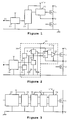
- FIG. 3 illustrates in general and in the form of blocks a circuit according to the present invention.
- This circuit comprises, on the side of the control circuit 10 referenced to ground, a pulse coder 40 and, on the side of the gate control circuit 20 referenced to the floating potential V F , a decoder 50 separated by a level translator circuit 30.
- the decoder has been illustrated at the entrance to circuit 20. In fact, it will be nested with this circuit to be placed behind the locations where parasitic pulses are likely to appear in order to be able to differentiate between the coded pulses coming from of the encoder 40 and of the parasitic pulses, as will appear more clearly on reading the description below.
- FIG. 4 An example of an encoder circuit 40 forming part of the control circuit 10 is illustrated in FIG. 4.
- This circuit 40 comprises a pulse generator oscillator 41 whose output is applied to the input C * of a counter 42.
- the signal command determining the circuit output appears on its IN input and goes from a low state to a high state when we want to determine switching on the power switch 1.
- the OUTA and OUTB outputs of this circuit appear at the output of OR gates O1 and O2.
- the signal IN is applied to the input of an AND gate A1 and, via an inverter I1, to the input of an AND gate A2.
- the output of gate A1 is sent to a first input of an OR gate O3, an AND gate A3, an AND gate A4 and an AND gate A5.
- the output of AND gate A2 is sent to the second input of OR gate O3, and to the first AND gate inputs A6, A7 and A8.
- the output of the AND gate A5 is sent to the input R of a D flip-flop type 43 and to the input C of a D flip-flop type D 44.
- the output of the AND gate A8 is sent to the input C of flip-flop 43 and at input R of flip-flop 44.
- the inputs D of these flip-flops 43 and 44 are fixed at a positive potential and the complementary outputs Q * of these flip-flops are respectively sent to each of the second inputs of the gates AND A1 and A2.
- the output of the OR gate O3 is sent to the input R * of the counter 42.
- the rank 0 output of this counter 42 is sent to a first input of an AND gate with three inputs A9 whose second and third inputs receive the outputs of rank 1 and 2 of the counter 42 via inverters I2 and I3.
- the fourth output of counter 42 is sent to the second inputs of doors A5 and A8.
- the row 0 output of counter 42 is also sent to the second inputs of doors A3 and A6.
- the output of door A9 is sent to the second inputs of doors A4 and A7.
- Gate O1 receives the outputs of gates A3 and A7 and gate O2 receives the outputs of gates A4 and A6.
- This signal (9) applied to doors A5 and A8 causes the signals (1) and (2) to change state (at the outputs Q * of flip-flops of type D 44 and 43). This results in a switching of the state of the output (3) of the AND gate A1 and therefore of the output (5) of the OR gate O3 and an inhibition of the counter 42. It can be seen that the OUTA output of the gate O1 corresponds to the signal (7) and that the OUTB output of the O2 gate corresponds to the signal (8). An OUTA signal consisting of four successive pulses and an OUTB signal consisting of a single pulse coinciding with the first pulse on the OUTA output is therefore finally obtained at the output of the circuit.
- FIG. 7 represents in a corresponding way the signals appearing at the input IN, at points (1) to (9) and on the outputs OUTA and OUTB when the signal IN goes from high to low level to determine the opening of the switch of power 1. This figure is self-explanatory after the detailed description made previously of FIG. 6.
- FIG. 7 shows that an opening order will correspond to the emission on the OUTA output of a pulse and on the OUTB output of a succession of four pulses, the first of which coincides with the pulse on the OUTA output.
- control signals supplied at the output of the encoder circuit 40 constitutes one of the aspects of the present invention.
- FIG. 5 represents an overall diagram of the circuit according to the present invention in which the decoding part has been more particularly detailed.
- the control circuit 10 providing an input signal IN to an encoder 40 provided with outputs OUTA and OUTB. These outputs are sent to level translators corresponding to the elements 31 to 34 of FIG. 3. These level translators send signals to the inputs S and R of a flip-flop 21 via a decoding circuit 50.
- the level translators 31, 33 and 32, 34 are conventional circuits, similar to those which would be used in the case of FIG. 2. They will therefore not be described here in detail. Their outputs are designated by the references OUT31 and OUT32. In the absence of interference, the signals on the outputs OUT32 and OUT31 correspond respectively to the output signals OUTA and OUTB of the encoder 40.
- the decoder 50 receives on its two inputs the signals OUT32 and OUT31.
- the signal OUT32 is sent via two successive inverters I11 and I12 to the input C of a counter 51 and the signal OUT31 is sent via two successive inverters I13 and I14 at input C of a D type flip-flop 52.
- the connection point of inverters I11 and I12 is connected to the first input of an AND gate A11, the second input of which is connected to the connection point inverters I13 and I14 and whose output is connected to the reset terminals R of counter 51 and flip-flop 52.
- the two outputs 0 and 1 of counter 51 are sent to two inputs of an AND gate A12 whose output is connected to the input S of the flip-flop 21.
- the Q output of the flip-flop 52 is sent to the R input of the flip-flop RS 21.
- the Q * output of the flip-flop 52 is sent to its input D.
- the closing signal resulting from the output of the counter 51 sent to the input S of the flip-flop 21 is delayed while the opening signal resulting from the output Q of the flip-flop 52 is sent on input R of flip-flop 21 and transmitted immediately.
- a slight delay is therefore inherently provided between a closing order and an opening order, this delay being adjustable with the frequency of the oscillation of the encoder 40. Since, as explained above, a circuit according to the present invention is intended to be inserted in a bridge control circuit, this avoids situations where two power switches of a bridge would be closed simultaneously which would cause risks of short circuit of an arm of the bridge.
- each of these elements could be replaced by an encoder / decoder to allow return from a floating power switch for information on its operating state.
Landscapes
- Electronic Switches (AREA)
- Analogue/Digital Conversion (AREA)
Claims (2)
- Steuer- und Überwachungsschaltung für einen Leistungsschalter, mit einem ersten Abschnitt (20), der mit diesem Schalter verbunden ist und der bezüglich einer Schwebespannung (VF) einer Elektrode dieses Schalters gespeist wird, einem zweiten Abschnitt (10), der mit externen Schaltungen mit dem Schalter verbunden ist und bezüglich einer festen Spannung gespeist wird, einem Codierer (40) der auf der Seite des zweiten Abschnittes angeordnet ist, und einem passenden Decodierer (50), der auf der Seite des ersten Abschnitts angeordnet ist, wobei die Verbindung zwischen den beiden Abschnitten über zwei Pfade gebildet wird, welche jeweils mit Eingängen R und S eines Flip-Flops (21) verbunden sind, das mit dem Ausgang des Decodierers (50) verbunden ist, dadurch gekennzeichnet, daß der Codierer eine Vorrichtung zum gleichzeitigen Senden mindestens eines Impulses auf jeden Pfad und dann mindestens eines Impulses auf einen ausgewählten Pfad aufweist, wobei der Decodierer geeignete Decodierungsmittel aufweist.
- Steuer- und Überwachungsschaltung nach Anspruch 1, dadurch gekennzeichnet, daß der erste und der zweite Abschnitt jeweils einen Codierer/Decodierer aufweisen.
Applications Claiming Priority (2)
| Application Number | Priority Date | Filing Date | Title |
|---|---|---|---|
| FR9000404A FR2656965B1 (fr) | 1990-01-09 | 1990-01-09 | Commande et controle d'un commutateur de puissance. |
| FR9000404 | 1990-01-09 |
Publications (2)
| Publication Number | Publication Date |
|---|---|
| EP0437409A1 EP0437409A1 (de) | 1991-07-17 |
| EP0437409B1 true EP0437409B1 (de) | 1995-09-27 |
Family
ID=9392774
Family Applications (1)
| Application Number | Title | Priority Date | Filing Date |
|---|---|---|---|
| EP91420003A Expired - Lifetime EP0437409B1 (de) | 1990-01-09 | 1991-01-07 | Betätigung und Steuerung eines Leistungsschalters |
Country Status (4)
| Country | Link |
|---|---|
| US (1) | US5134322A (de) |
| EP (1) | EP0437409B1 (de) |
| DE (1) | DE69113286T2 (de) |
| FR (1) | FR2656965B1 (de) |
Families Citing this family (17)
| Publication number | Priority date | Publication date | Assignee | Title |
|---|---|---|---|---|
| US5274274A (en) * | 1992-03-23 | 1993-12-28 | Power Integrations, Inc. | Dual threshold differential discriminator |
| US5545955A (en) * | 1994-03-04 | 1996-08-13 | International Rectifier Corporation | MOS gate driver for ballast circuits |
| US5550436A (en) * | 1994-09-01 | 1996-08-27 | International Rectifier Corporation | MOS gate driver integrated circuit for ballast circuits |
| DE69403964T2 (de) * | 1994-09-16 | 1998-01-29 | Sgs Thomson Microelectronics | Steuerschaltung mit einem Pegelschieber zum Schalten eines eletronischen Schalters |
| EP0703667B1 (de) * | 1994-09-16 | 1997-06-25 | STMicroelectronics S.r.l. | Integrierte Steuerschaltungsanordnung mit einem Pegelschieber zum Schalten eines elektronischen Schalters |
| FR2726426B1 (fr) * | 1994-10-28 | 1996-11-29 | Sgs Thomson Microelectronics | Starter electronique pour lampe fluorescente |
| US5543740A (en) * | 1995-04-10 | 1996-08-06 | Philips Electronics North America Corporation | Integrated half-bridge driver circuit |
| EP0764365A2 (de) * | 1995-04-10 | 1997-03-26 | Koninklijke Philips Electronics N.V. | Pegelschieber und damit ausgerüsteter treiber für die seite mit den hohen spannungen |
| US5719521A (en) * | 1996-10-29 | 1998-02-17 | Philips Electronics North America Corporation | Integrated half-bridge timing control circuit |
| GB2324664B (en) * | 1997-04-23 | 2001-06-27 | Int Rectifier Corp | Resistor in series with bootstrap diode for monolithic gate device |
| JP3635975B2 (ja) * | 1999-03-02 | 2005-04-06 | 富士電機デバイステクノロジー株式会社 | レベルシフト回路 |
| JP3773863B2 (ja) * | 2001-07-19 | 2006-05-10 | 三菱電機株式会社 | 半導体装置 |
| JP4382312B2 (ja) * | 2001-09-05 | 2009-12-09 | 三菱電機株式会社 | 駆動制御装置、電力変換装置、電力変換装置の制御方法、および電力変換装置の使用方法 |
| JP3770836B2 (ja) * | 2002-01-23 | 2006-04-26 | 株式会社ルネサステクノロジ | 高速に電源スイッチのオンオフが可能な論理回路及び同論理回路における電流低減方法 |
| US7053692B2 (en) * | 2002-12-19 | 2006-05-30 | United Memories, Inc. | Powergate control using boosted and negative voltages |
| JP2008516543A (ja) * | 2004-10-12 | 2008-05-15 | コーニンクレッカ フィリップス エレクトロニクス エヌ ヴィ | レーザまたは変調器駆動用の低電圧高速出力段 |
| CN105743079B (zh) * | 2016-04-07 | 2018-01-16 | 中国南方电网有限责任公司超高压输电公司检修试验中心 | 一种防止高压直流工程自动解锁系统 |
Family Cites Families (8)
| Publication number | Priority date | Publication date | Assignee | Title |
|---|---|---|---|---|
| US4039862A (en) * | 1976-01-19 | 1977-08-02 | Rca Corporation | Level shift circuit |
| EP0153423B1 (de) * | 1984-02-20 | 1988-02-10 | HONEYWELL BULL ITALIA S.p.A. | Treiberschaltung für einen Leistungs-FET |
| US4697107A (en) * | 1986-07-24 | 1987-09-29 | National Semiconductor Corporation | Four-state I/O control circuit |
| JPS63133819A (ja) * | 1986-11-11 | 1988-06-06 | シーメンス、アクチエンゲゼルシヤフト | 自己保護性電力開閉器の回路装置 |
| US4862018A (en) * | 1987-11-30 | 1989-08-29 | Texas Instruments Incorporated | Noise reduction for output drivers |
| US4864158A (en) * | 1988-01-28 | 1989-09-05 | Amtech Corporation | Rapid signal validity checking apparatus |
| IT1221251B (it) * | 1988-02-25 | 1990-06-27 | Sgs Thomson Microelectronics | Circuito mos per il pilotaggio di un carico dal lato alto della alimentazione |
| US5025182A (en) * | 1990-08-31 | 1991-06-18 | Advanced Micro Devices, Inc. | Digital apparatus for generating gating signals in response to a data signal |
-
1990
- 1990-01-09 FR FR9000404A patent/FR2656965B1/fr not_active Expired - Fee Related
-
1991
- 1991-01-07 US US07/637,918 patent/US5134322A/en not_active Ceased
- 1991-01-07 EP EP91420003A patent/EP0437409B1/de not_active Expired - Lifetime
- 1991-01-07 DE DE69113286T patent/DE69113286T2/de not_active Expired - Lifetime
Also Published As
| Publication number | Publication date |
|---|---|
| DE69113286T2 (de) | 1996-05-09 |
| DE69113286D1 (de) | 1995-11-02 |
| EP0437409A1 (de) | 1991-07-17 |
| US5134322A (en) | 1992-07-28 |
| FR2656965B1 (fr) | 1995-01-20 |
| FR2656965A1 (fr) | 1991-07-12 |
Similar Documents
| Publication | Publication Date | Title |
|---|---|---|
| EP0437409B1 (de) | Betätigung und Steuerung eines Leistungsschalters | |
| EP1085659B1 (de) | Digital-Analog-Wandler des Stromtyps | |
| EP0785646B1 (de) | Bidirektionaler Relaisverstärker | |
| FR2466906A1 (fr) | Circuit detecteur de transitions d'un niveau de signal a un autre | |
| FR2756986A1 (fr) | Circuits et procedes de commande de moteur a courant continu, sans balai, triphase, utilisant un seul signal hall | |
| FR2699023A1 (fr) | Circuit à retard commandé. | |
| FR2573211A1 (fr) | Comparateur synchronise | |
| FR2473814A1 (fr) | Circuit mos dynamique ne dependant pas d'un rapport de resistances destine a constituer des circuits logiques divers | |
| EP0562905A1 (de) | Schaltung mit veränderlicher Verzögerung | |
| FR2692072A1 (fr) | Bascule bistable à commande de réinitialisation. | |
| FR2806555A1 (fr) | Generateur de nombres pseudo-aleatoires | |
| EP0901227A1 (de) | Schaltung mit variabler Verzögerung | |
| EP0037315A1 (de) | Steuerungsanordnung der Helligkeitsänderungen einer Lichtanlage im Laufe der Zeit | |
| EP0442829A1 (de) | Taktfrequenzverdoppler | |
| EP3015870B1 (de) | Messvorrichtung eines zerhackten stroms | |
| FR2625346A1 (fr) | Agencement capacitif commute | |
| EP0863512A1 (de) | Doppelzugriffspeicher | |
| EP3667915A1 (de) | Verzögerungsschaltkreis | |
| EP0283393A1 (de) | Binäre Rechnungseinrichtung | |
| CA2057824C (fr) | Dispositif de retard reglable | |
| EP0537083B1 (de) | Vorrichtung zum Lesen eines Speicherzelleinhalts, insbesondere für ein EPROM, Betriebsverfahren und Speicher mit einer solchen Vorrichtung | |
| FR2588088A1 (fr) | Dispositif de generation de signaux de temps | |
| JPH09511855A (ja) | 切替電流微分器 | |
| FR2781621A1 (fr) | Amplificateur de sortie cmos independant de la temperature, de la tension d'alimentation et de la qualite de fabrication de ses transistors | |
| EP3182617B1 (de) | Optischer empfänger mit relativer phasendetektion |
Legal Events
| Date | Code | Title | Description |
|---|---|---|---|
| PUAI | Public reference made under article 153(3) epc to a published international application that has entered the european phase |
Free format text: ORIGINAL CODE: 0009012 |
|
| AK | Designated contracting states |
Kind code of ref document: A1 Designated state(s): DE FR GB IT |
|
| 17P | Request for examination filed |
Effective date: 19911218 |
|
| 17Q | First examination report despatched |
Effective date: 19940614 |
|
| GRAA | (expected) grant |
Free format text: ORIGINAL CODE: 0009210 |
|
| AK | Designated contracting states |
Kind code of ref document: B1 Designated state(s): DE FR GB IT |
|
| ITF | It: translation for a ep patent filed |
Owner name: MARCHI & MITTLER S.R.L. |
|
| REF | Corresponds to: |
Ref document number: 69113286 Country of ref document: DE Date of ref document: 19951102 |
|
| GBT | Gb: translation of ep patent filed (gb section 77(6)(a)/1977) |
Effective date: 19951017 |
|
| PLBE | No opposition filed within time limit |
Free format text: ORIGINAL CODE: 0009261 |
|
| STAA | Information on the status of an ep patent application or granted ep patent |
Free format text: STATUS: NO OPPOSITION FILED WITHIN TIME LIMIT |
|
| 26N | No opposition filed | ||
| REG | Reference to a national code |
Ref country code: GB Ref legal event code: IF02 |
|
| PGFP | Annual fee paid to national office [announced via postgrant information from national office to epo] |
Ref country code: GB Payment date: 20091229 Year of fee payment: 20 |
|
| PGFP | Annual fee paid to national office [announced via postgrant information from national office to epo] |
Ref country code: FR Payment date: 20100223 Year of fee payment: 20 Ref country code: IT Payment date: 20100121 Year of fee payment: 20 |
|
| PGFP | Annual fee paid to national office [announced via postgrant information from national office to epo] |
Ref country code: DE Payment date: 20091230 Year of fee payment: 20 |
|
| REG | Reference to a national code |
Ref country code: GB Ref legal event code: PE20 Expiry date: 20110106 |
|
| PG25 | Lapsed in a contracting state [announced via postgrant information from national office to epo] |
Ref country code: GB Free format text: LAPSE BECAUSE OF EXPIRATION OF PROTECTION Effective date: 20110106 |
|
| PG25 | Lapsed in a contracting state [announced via postgrant information from national office to epo] |
Ref country code: DE Free format text: LAPSE BECAUSE OF EXPIRATION OF PROTECTION Effective date: 20110107 |