EP0436812B1 - Procédé de décapage du cuivre et circuit imprimé fabriqué par ce procédé - Google Patents
Procédé de décapage du cuivre et circuit imprimé fabriqué par ce procédé Download PDFInfo
- Publication number
- EP0436812B1 EP0436812B1 EP90122376A EP90122376A EP0436812B1 EP 0436812 B1 EP0436812 B1 EP 0436812B1 EP 90122376 A EP90122376 A EP 90122376A EP 90122376 A EP90122376 A EP 90122376A EP 0436812 B1 EP0436812 B1 EP 0436812B1
- Authority
- EP
- European Patent Office
- Prior art keywords
- copper
- organic
- chamber
- substrate
- radical
- Prior art date
- Legal status (The legal status is an assumption and is not a legal conclusion. Google has not performed a legal analysis and makes no representation as to the accuracy of the status listed.)
- Expired - Lifetime
Links
- 239000010949 copper Substances 0.000 title claims description 77
- 229910052802 copper Inorganic materials 0.000 title claims description 71
- RYGMFSIKBFXOCR-UHFFFAOYSA-N Copper Chemical compound [Cu] RYGMFSIKBFXOCR-UHFFFAOYSA-N 0.000 title claims description 61
- 238000000034 method Methods 0.000 title claims description 56
- -1 amine compounds Chemical class 0.000 claims description 16
- 239000000758 substrate Substances 0.000 claims description 16
- 239000007795 chemical reaction product Substances 0.000 claims description 8
- 238000005530 etching Methods 0.000 claims description 8
- 238000001465 metallisation Methods 0.000 claims description 8
- 238000010438 heat treatment Methods 0.000 claims description 7
- INQOMBQAUSQDDS-UHFFFAOYSA-N iodomethane Chemical compound IC INQOMBQAUSQDDS-UHFFFAOYSA-N 0.000 claims description 5
- XLYOFNOQVPJJNP-UHFFFAOYSA-N water Substances O XLYOFNOQVPJJNP-UHFFFAOYSA-N 0.000 claims description 5
- 125000000217 alkyl group Chemical group 0.000 claims description 2
- 230000000873 masking effect Effects 0.000 claims description 2
- VSQYNPJPULBZKU-UHFFFAOYSA-N mercury xenon Chemical compound [Xe].[Hg] VSQYNPJPULBZKU-UHFFFAOYSA-N 0.000 claims description 2
- 238000005406 washing Methods 0.000 claims description 2
- 239000004020 conductor Substances 0.000 claims 2
- 230000001678 irradiating effect Effects 0.000 claims 2
- 230000005855 radiation Effects 0.000 claims 2
- 150000001875 compounds Chemical class 0.000 claims 1
- 238000001914 filtration Methods 0.000 claims 1
- 125000001997 phenyl group Chemical group [H]C1=C([H])C([H])=C(*)C([H])=C1[H] 0.000 claims 1
- 239000010408 film Substances 0.000 description 16
- 235000012431 wafers Nutrition 0.000 description 15
- 239000000047 product Substances 0.000 description 13
- 150000003254 radicals Chemical class 0.000 description 12
- 238000006243 chemical reaction Methods 0.000 description 11
- 238000004519 manufacturing process Methods 0.000 description 10
- 238000009792 diffusion process Methods 0.000 description 5
- 229910052782 aluminium Inorganic materials 0.000 description 4
- XAGFODPZIPBFFR-UHFFFAOYSA-N aluminium Chemical compound [Al] XAGFODPZIPBFFR-UHFFFAOYSA-N 0.000 description 4
- 238000010494 dissociation reaction Methods 0.000 description 4
- 230000005593 dissociations Effects 0.000 description 4
- 239000000376 reactant Substances 0.000 description 4
- 150000001412 amines Chemical class 0.000 description 3
- 230000004888 barrier function Effects 0.000 description 3
- 239000000463 material Substances 0.000 description 3
- VYPSYNLAJGMNEJ-UHFFFAOYSA-N silicon dioxide Inorganic materials O=[Si]=O VYPSYNLAJGMNEJ-UHFFFAOYSA-N 0.000 description 3
- 238000004544 sputter deposition Methods 0.000 description 3
- CSCPPACGZOOCGX-UHFFFAOYSA-N Acetone Chemical compound CC(C)=O CSCPPACGZOOCGX-UHFFFAOYSA-N 0.000 description 2
- ZAMOUSCENKQFHK-UHFFFAOYSA-N Chlorine atom Chemical compound [Cl] ZAMOUSCENKQFHK-UHFFFAOYSA-N 0.000 description 2
- 239000005749 Copper compound Substances 0.000 description 2
- XUIMIQQOPSSXEZ-UHFFFAOYSA-N Silicon Chemical compound [Si] XUIMIQQOPSSXEZ-UHFFFAOYSA-N 0.000 description 2
- 230000015572 biosynthetic process Effects 0.000 description 2
- 239000003795 chemical substances by application Substances 0.000 description 2
- 229910052801 chlorine Inorganic materials 0.000 description 2
- 239000000460 chlorine Substances 0.000 description 2
- 150000001880 copper compounds Chemical class 0.000 description 2
- 238000001493 electron microscopy Methods 0.000 description 2
- 238000005516 engineering process Methods 0.000 description 2
- 229910052736 halogen Inorganic materials 0.000 description 2
- 238000011835 investigation Methods 0.000 description 2
- 238000000206 photolithography Methods 0.000 description 2
- 229920000642 polymer Polymers 0.000 description 2
- 229910052710 silicon Inorganic materials 0.000 description 2
- 239000010703 silicon Substances 0.000 description 2
- 235000012239 silicon dioxide Nutrition 0.000 description 2
- 239000002904 solvent Substances 0.000 description 2
- 238000006557 surface reaction Methods 0.000 description 2
- 239000004215 Carbon black (E152) Substances 0.000 description 1
- GRYLNZFGIOXLOG-UHFFFAOYSA-N Nitric acid Chemical compound O[N+]([O-])=O GRYLNZFGIOXLOG-UHFFFAOYSA-N 0.000 description 1
- 239000002253 acid Substances 0.000 description 1
- 238000000637 aluminium metallisation Methods 0.000 description 1
- 238000013459 approach Methods 0.000 description 1
- 238000009835 boiling Methods 0.000 description 1
- 239000013590 bulk material Substances 0.000 description 1
- NEHMKBQYUWJMIP-UHFFFAOYSA-N chloromethane Chemical compound ClC NEHMKBQYUWJMIP-UHFFFAOYSA-N 0.000 description 1
- 239000000356 contaminant Substances 0.000 description 1
- 238000011109 contamination Methods 0.000 description 1
- 230000001419 dependent effect Effects 0.000 description 1
- 238000011161 development Methods 0.000 description 1
- 238000001312 dry etching Methods 0.000 description 1
- 238000001035 drying Methods 0.000 description 1
- 150000002367 halogens Chemical class 0.000 description 1
- 231100001261 hazardous Toxicity 0.000 description 1
- 229930195733 hydrocarbon Natural products 0.000 description 1
- 150000002430 hydrocarbons Chemical class 0.000 description 1
- 230000003993 interaction Effects 0.000 description 1
- 238000010849 ion bombardment Methods 0.000 description 1
- 239000007788 liquid Substances 0.000 description 1
- 238000002844 melting Methods 0.000 description 1
- 230000008018 melting Effects 0.000 description 1
- 229910052751 metal Inorganic materials 0.000 description 1
- 239000002184 metal Substances 0.000 description 1
- 229910021421 monocrystalline silicon Inorganic materials 0.000 description 1
- 229910017604 nitric acid Inorganic materials 0.000 description 1
- 238000006053 organic reaction Methods 0.000 description 1
- 239000002245 particle Substances 0.000 description 1
- 238000000059 patterning Methods 0.000 description 1
- 229920002120 photoresistant polymer Polymers 0.000 description 1
- 238000001020 plasma etching Methods 0.000 description 1
- 238000012545 processing Methods 0.000 description 1
- 230000001681 protective effect Effects 0.000 description 1
- 239000010453 quartz Substances 0.000 description 1
- 239000004065 semiconductor Substances 0.000 description 1
- 239000000377 silicon dioxide Substances 0.000 description 1
- 239000007787 solid Substances 0.000 description 1
- 238000000992 sputter etching Methods 0.000 description 1
- 239000010409 thin film Substances 0.000 description 1
- MAKDTFFYCIMFQP-UHFFFAOYSA-N titanium tungsten Chemical compound [Ti].[W] MAKDTFFYCIMFQP-UHFFFAOYSA-N 0.000 description 1
- 239000011800 void material Substances 0.000 description 1
- 239000002699 waste material Substances 0.000 description 1
Images

Classifications
-
- C—CHEMISTRY; METALLURGY
- C23—COATING METALLIC MATERIAL; COATING MATERIAL WITH METALLIC MATERIAL; CHEMICAL SURFACE TREATMENT; DIFFUSION TREATMENT OF METALLIC MATERIAL; COATING BY VACUUM EVAPORATION, BY SPUTTERING, BY ION IMPLANTATION OR BY CHEMICAL VAPOUR DEPOSITION, IN GENERAL; INHIBITING CORROSION OF METALLIC MATERIAL OR INCRUSTATION IN GENERAL
- C23F—NON-MECHANICAL REMOVAL OF METALLIC MATERIAL FROM SURFACE; INHIBITING CORROSION OF METALLIC MATERIAL OR INCRUSTATION IN GENERAL; MULTI-STEP PROCESSES FOR SURFACE TREATMENT OF METALLIC MATERIAL INVOLVING AT LEAST ONE PROCESS PROVIDED FOR IN CLASS C23 AND AT LEAST ONE PROCESS COVERED BY SUBCLASS C21D OR C22F OR CLASS C25
- C23F4/00—Processes for removing metallic material from surfaces, not provided for in group C23F1/00 or C23F3/00
- C23F4/02—Processes for removing metallic material from surfaces, not provided for in group C23F1/00 or C23F3/00 by evaporation
-
- H—ELECTRICITY
- H01—ELECTRIC ELEMENTS
- H01L—SEMICONDUCTOR DEVICES NOT COVERED BY CLASS H10
- H01L21/00—Processes or apparatus adapted for the manufacture or treatment of semiconductor or solid state devices or of parts thereof
-
- H—ELECTRICITY
- H05—ELECTRIC TECHNIQUES NOT OTHERWISE PROVIDED FOR
- H05K—PRINTED CIRCUITS; CASINGS OR CONSTRUCTIONAL DETAILS OF ELECTRIC APPARATUS; MANUFACTURE OF ASSEMBLAGES OF ELECTRICAL COMPONENTS
- H05K3/00—Apparatus or processes for manufacturing printed circuits
- H05K3/02—Apparatus or processes for manufacturing printed circuits in which the conductive material is applied to the surface of the insulating support and is thereafter removed from such areas of the surface which are not intended for current conducting or shielding
Definitions
- the invention concerns methods for etching copper layers, especially copper layers overlying a layer of a second material, such as found in printed circuit fabrication and the seed copper layers used in printed circuit fabrication and in integrated circuit metallization layers, by photo-formed and photo-activated organic and amine radicals.
- Patterned etching of copper films has been accomplished, primarily in printed circuit fabrication, by wet processes wherein a protective, patterned film, such as a photoresist is applied to a copper layer and then a strong liquid etchant, usually an acid, is applied to etch the exposed copper down to the base material.
- a protective, patterned film such as a photoresist
- a strong liquid etchant usually an acid
- This process presents several problems when applied to integrated circuit fabrication, such as the following.
- the wet processes are inherently "dirty" in that contaminants in the etchant can be introduced to the integrated circuit wafer.
- the wet etchants required are generally hazardous to operators by contact and inhalation of vapors produced thereby.
- Etching of copper requires etchants, high temperatures, or both which may damage the other layers of an integrated circuit.
- Etching of copper by wet processes is isotropic, making copper metallization for VLSI circuits extremely difficult due to inadequate critical dimension definition and control. Dispos
- Sputtering techniques are utilized presently to remove copper from copper-doped aluminum films and therefore may have application to removing copper films.
- sputtering the physical dislodging of copper atoms and clusters by high energy ion bombardment, does not exhibit selective removal of various films and will result in extreme build-up of residue in the reaction chamber, since copper is not converted to a volatile species.
- sputter removal techniques are relatively slow, difficult to control, and exhibit insufficient selectivity to patterned masking layers and underlying thin films.
- Dry etch processes involving a plasma to form reactive agents such as a halogen, an amine, or an organic radical which react and form volatile copper products could be an approach to an effective etch process for copper which solves some of the problems encountered in other processes, particularly the redeposit of residue on reaction chambers.
- reactive agents such as a halogen, an amine, or an organic radical which react and form volatile copper products
- a plasma discharge produces a wide range of disassociated, reactive products that can combine homogeneously or heterogeneously to form a polymer residue. For example, hydrocarbon and chlorocarbon discharges produce heavy residues of polymer. The residue generates many particles.
- the Inventor has discovered that, especially at higher substrate or chamber temperatures, anisotropic volatilization of the copper amine or organic reaction product from unmasked areas is possible to achieve anisotropic dry etching of copper film. And, further, even when the copper amine or organic product is not volatile, complete reaction of a bulk copper film with the radical directionally or anisotropically occurs directionally or anisotropically to produce a copper amine or organo-copper reaction product which is easily removed anisotropically by a solvent or water wash. Most importantly, the copper amine or organic product is formed anisotropically so whether the product is removed by volatilization or wet solution, the patterned copper is not removed or undercut isotropically.
- Figure 1 is a schematic drawing of an embodiment of a reaction chamber as used in the process according to the instant invention.
- Figures 2a and 2b are drawings representative of side views by electron microscopy of a semiconductor wafer during two stages of the etch process according to the instant invention.
- a sealed chamber 6 having a substrate holder 8, which normally has temperature controlled heating elements (not shown) for heating a substrate placed thereon.
- Mask 11 in integrated circuit fabrication processes, would typically be a photo sensitive mask material of known types which is patterned and etched according to well-known photolithographic techniques. However, mask 11 may also be fabricated by techniques other than photolithography.
- Substrate holder 8 may contain controlled heating elements (not shown) for the purpose of heating the substrate 9 to a desired process temperature. The process temperature desired may be determined according to several factors.
- a high process temperature is required. The exact temperature required is dependent upon the radical agent used. However, factored against utilization of such high process temperatures is the fact that the integrated circuit wafers processed may be damaged or destroyed by the temperatures required for significant volatilization. Of course, printed circuit substrates may not be so damaged by high process temperatures.
- a high intensity light source 4 such as a filtered ultra violet source, e.g., a 1000 watt Hg/Xe lamp, is located above the chamber 6. Focusing elements 2 and 3 are arranged to direct the high intensity light through transparent window 7, which may be a quartz window, onto the surface of the masked copper layer 10 and 11. The window 7 is sealed, as by "0"-ring 14. It is pointed out that, although Figure 1 shows the high intensity light directed perpendicularly to the wafer, it has been found to be also effective if the chamber is arranged so that the light is directed at other angles to, and even parallel to, the wafer.
- a filtered ultra violet source e.g., a 1000 watt Hg/Xe lamp
- Reactant R is an amine radical or organic radical, such as alkyl or phenyl radicals.
- the radical may be produced from an organic or amine compound, e.g., CH3I by photochemical dissociation, microwave afterglow dissociation or plasma discharge dissociation, for example, as is known in the art.
- the halogen radical may be produced within the chamber by photochemical dissociation by, for example, introducing CH3I to the high intensity ultraviolet light 5 from source 4.
- the organic or amine radical R is then light activated by high intensity light 5 and contacts the copper layer 10 and mask layer 11.
- the etch process which occurs within the chamber 6, will follow two different methodologies, depending primarily upon the temperature at which the process occurs and the reactant used.
- An amine or organic parent molecule, P is photo-dissociated to form radical species R.
- reactant radical R the copper and radicals react at the surface to form a copper amine or organic copper compound.
- product CuR is not volatile, the product remains on the copper layer surface. Surprisingly however, the Inventor has found that the reaction continues throughout the copper layer to form CuR. The surface reaction does not block reaction beneath the surface under the process conditions disclosed. After the reaction has then occurred throughout the copper layer 10, the resulting copper amine or organo-copper product CuR can be washed away using an appropriate solution such as water or acetone. The copper amine or organo-copper product will easily enter into solution.
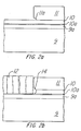
- Figures 2a and 2b show a representation of an integrated circuit wafer using a copper metallization layer during two stages of the process according to the invention as has been observed by electron microscopy.
- the wafer of Figure 2a is shown before the etch process showing a silicon substrate 9, a silicon dioxide layer 9a, a titanium tungsten barrier layer 10a, and a copper layer 10.
- a mask layer 11 is applied and patterned by well-known photolithography methods, for example, or by other known means.
- a cantilevered resist overhang 11a is generated by an image-reversal development process.
- Figure 2b depicts the same wafer after etch processing steps have been accomplished, as in the chamber of Figure 1, under the following conditions.
- the wafer (9, 10 and 11) may be deglazed as by a dilute nitric acid.
- a 1000 watt Mercury-Xenon lamp with a water filter was directed upon the wafer 9, 10 and 11.
- the water filter serves to extract most of the infrared light above 1.3nm while passing the deep ultraviolet light, down to 200 nm.
- the light was directed orthogonally to the wafer.
- the wafer was heated to a temperature of above 200°C.
- CH3I was introduced to the chamber, at 10 torr, at the rate of 100 sccm.
- the CH3 was dissociated by the photo energy of the light source.
- Figure 2b shows that the entire copper layer which was not masked has reacted and expanded to about three times its previous thickness.
- the resulting product layer film 12 was found to be Cu(CH3)2. Further, a void 14, can be noted.
- the resulting film may be removed by a simple wash step.
Landscapes
- Engineering & Computer Science (AREA)
- Chemical & Material Sciences (AREA)
- Manufacturing & Machinery (AREA)
- Materials Engineering (AREA)
- Physics & Mathematics (AREA)
- Computer Hardware Design (AREA)
- Microelectronics & Electronic Packaging (AREA)
- Power Engineering (AREA)
- Condensed Matter Physics & Semiconductors (AREA)
- General Physics & Mathematics (AREA)
- Mechanical Engineering (AREA)
- Metallurgy (AREA)
- Organic Chemistry (AREA)
- Manufacturing Of Printed Circuit Boards (AREA)
- Internal Circuitry In Semiconductor Integrated Circuit Devices (AREA)
- Drying Of Semiconductors (AREA)
- ing And Chemical Polishing (AREA)
- Cleaning Or Drying Semiconductors (AREA)
Claims (9)
- Procédé de décapage d'une couche de cuivre sur un substrat pour former une configuration de conducteurs, comportant les étapes qui consistent :
à placer le substrat dans une chambre fermée ;
à masquer les zones de ladite couche de cuivre ne devant pas être décapées ;
à introduire un corps chimique produisant un radical organique choisi dans le groupe des composés comprenant les composés d'alkyles, de phényles et d'amines dans ladite chambre, de telle sorte que les zones non masquées du cuivre soient exposées au corps chimique produisant un radical organique ;
à soumettre ladite chambre à un faisceau de rayonnements ultraviolets de haute intensité, de telle sorte que le radical organique soit formé et réagisse avec ledit cuivre exposé afin de former un produit de réaction constitué par un composé organique du cuivre ; et
à retirer ledit produit de réaction constitué par un composé organique cuivre, laissant ainsi une configuration de conducteurs en cuivre. - Procédé selon la revendication 1, comportant en outre l'étape qui consiste à chauffer ledit substrat à une température à laquelle ledit produit de réaction constitué par un composé organique du cuivre est sensiblement volatil.
- Procédé selon la revendication 2, dans lequel ladite étape de chauffage comporte le chauffage dudit substrat à une température supérieure à 200°C.
- Procédé selon la revendication 1, comportant en outre l'étape qui consiste à laver ledit substrat pour retirer le produit de réaction constitué par un composé organique du cuivre.
- Procédé selon l'une quelconque des revendications précédentes, dans lequel on utilise du CH₃I comme corps chimique produisant un radical organique.
- Procédé selon la revendication 5, comportant en outre les étapes qui consistent à introduire ledit CH₃I dans ladite chambre sous une pression de 10 torr ; à soumettre la chambre à un rayonnement en utilisant une lampe au mercure-xénon de 1000 W adaptée pour produire un faisceau de rayonnement dans un intervalle de longueur d'onde compris entre 1,3 nm à 200 nm, créant ainsi le radical CH₃ ; à exposer la plaque au radical CH₃ pendant environ quinze minutes, produisant ainsi le produit de réaction constitué par un composé organique du cuivre, Cu(CH₃)₂.
- Procédé selon la revendication 6, comportant en outre la production dudit faisceau dans ledit intervalle de longueur d'onde en filtrant le rayonnement provenant de la lumière à travers un filtre à eau.
- Circuit imprimé comportant une métallisation formée par le procédé suivant l'une quelconque des revendications précédentes.
- Circuit intégré comportant une métallisation formée par le procédé suivant l'une quelconque des revendications 1 à 7.
Applications Claiming Priority (2)
| Application Number | Priority Date | Filing Date | Title |
|---|---|---|---|
| US453543 | 1982-12-27 | ||
| US45354389A | 1989-12-20 | 1989-12-20 |
Publications (2)
| Publication Number | Publication Date |
|---|---|
| EP0436812A1 EP0436812A1 (fr) | 1991-07-17 |
| EP0436812B1 true EP0436812B1 (fr) | 1994-08-31 |
Family
ID=23800973
Family Applications (1)
| Application Number | Title | Priority Date | Filing Date |
|---|---|---|---|
| EP90122376A Expired - Lifetime EP0436812B1 (fr) | 1989-12-20 | 1990-11-23 | Procédé de décapage du cuivre et circuit imprimé fabriqué par ce procédé |
Country Status (4)
| Country | Link |
|---|---|
| EP (1) | EP0436812B1 (fr) |
| JP (1) | JP3313374B2 (fr) |
| KR (1) | KR100194297B1 (fr) |
| DE (1) | DE69012084T2 (fr) |
Family Cites Families (5)
| Publication number | Priority date | Publication date | Assignee | Title |
|---|---|---|---|---|
| DE3376186D1 (en) * | 1983-08-02 | 1988-05-05 | Ibm Deutschland | Dry-etching process and its use |
| US4490210A (en) * | 1984-01-24 | 1984-12-25 | International Business Machines Corporation | Laser induced dry chemical etching of metals |
| JPH0642456B2 (ja) * | 1984-11-21 | 1994-06-01 | 株式会社日立製作所 | 表面光処理方法 |
| JPS61187237A (ja) * | 1985-02-14 | 1986-08-20 | Toshiba Corp | パタ−ン形成方法 |
| US4622095A (en) * | 1985-10-18 | 1986-11-11 | Ibm Corporation | Laser stimulated halogen gas etching of metal substrates |
-
1990
- 1990-11-23 DE DE69012084T patent/DE69012084T2/de not_active Expired - Fee Related
- 1990-11-23 EP EP90122376A patent/EP0436812B1/fr not_active Expired - Lifetime
- 1990-12-19 KR KR1019900021072A patent/KR100194297B1/ko not_active IP Right Cessation
- 1990-12-20 JP JP40446090A patent/JP3313374B2/ja not_active Expired - Fee Related
Also Published As
| Publication number | Publication date |
|---|---|
| KR100194297B1 (ko) | 1999-06-15 |
| JPH03291387A (ja) | 1991-12-20 |
| DE69012084T2 (de) | 1995-01-19 |
| JP3313374B2 (ja) | 2002-08-12 |
| DE69012084D1 (de) | 1994-10-06 |
| EP0436812A1 (fr) | 1991-07-17 |
| KR910013441A (ko) | 1991-08-08 |
Similar Documents
| Publication | Publication Date | Title |
|---|---|---|
| US5100499A (en) | Copper dry etch process using organic and amine radicals | |
| EP0433983B1 (fr) | Procédé de gravure de cuivre utilisant des haloides | |
| US5910453A (en) | Deep UV anti-reflection coating etch | |
| EP0714119B1 (fr) | Procédé pour former un motif et procédé de préparation d'un composant semi-conducteur utilisant ledit procédé | |
| US5814238A (en) | Method for dry etching of transition metals | |
| US4444618A (en) | Processes and gas mixtures for the reactive ion etching of aluminum and aluminum alloys | |
| EP0489179B1 (fr) | Procede de fabrication d'un circuit integre a semi-conducteurs | |
| EP0234387A2 (fr) | Procédé d'élimination d'une photoréserve sur une plaquette semi-conductrice | |
| JPH09251989A (ja) | 水素ガスを用いた集積回路のプラズマ洗浄方法 | |
| JP3378055B2 (ja) | 異方性液相光化学銅エッチング | |
| EP1344113A2 (fr) | Procede de retrait de photoresine apres une implantation ionique | |
| US4132586A (en) | Selective dry etching of substrates | |
| US5851302A (en) | Method for dry etching sidewall polymer | |
| JPH08172077A (ja) | ビアのプラズマエッチング改良方法 | |
| EP0595053A2 (fr) | Méthode photochimique de gravure anisotrope en phase liquide | |
| JPH01214074A (ja) | 超伝導性酸化物材料薄膜の製造方法 | |
| US6162733A (en) | Method for removing contaminants from integrated circuits | |
| US5236550A (en) | Method for plasma etch of ruthenium | |
| US5041362A (en) | Dry developable resist etch chemistry | |
| US5318662A (en) | Copper etch process using halides | |
| KR20030093186A (ko) | 비아를 형성하는 과정에서 나온 에칭 잔여물을 제거하기위한 방법 | |
| EP0436812B1 (fr) | Procédé de décapage du cuivre et circuit imprimé fabriqué par ce procédé | |
| JPH07273093A (ja) | プラズマエッチング方法 | |
| EP0058214B1 (fr) | Méthode pour augmenter la résistance de la surface d'un matériau solide à la gravure | |
| JPH07201856A (ja) | 銅配線の形成方法 |
Legal Events
| Date | Code | Title | Description |
|---|---|---|---|
| PUAI | Public reference made under article 153(3) epc to a published international application that has entered the european phase |
Free format text: ORIGINAL CODE: 0009012 |
|
| AK | Designated contracting states |
Kind code of ref document: A1 Designated state(s): DE FR GB IT NL |
|
| 17P | Request for examination filed |
Effective date: 19920117 |
|
| 17Q | First examination report despatched |
Effective date: 19930113 |
|
| GRAA | (expected) grant |
Free format text: ORIGINAL CODE: 0009210 |
|
| AK | Designated contracting states |
Kind code of ref document: B1 Designated state(s): DE FR GB IT NL |
|
| ITF | It: translation for a ep patent filed | ||
| REF | Corresponds to: |
Ref document number: 69012084 Country of ref document: DE Date of ref document: 19941006 |
|
| ET | Fr: translation filed | ||
| PLBE | No opposition filed within time limit |
Free format text: ORIGINAL CODE: 0009261 |
|
| STAA | Information on the status of an ep patent application or granted ep patent |
Free format text: STATUS: NO OPPOSITION FILED WITHIN TIME LIMIT |
|
| 26N | No opposition filed | ||
| REG | Reference to a national code |
Ref country code: GB Ref legal event code: IF02 |
|
| PGFP | Annual fee paid to national office [announced via postgrant information from national office to epo] |
Ref country code: NL Payment date: 20041006 Year of fee payment: 15 |
|
| PGFP | Annual fee paid to national office [announced via postgrant information from national office to epo] |
Ref country code: FR Payment date: 20041105 Year of fee payment: 15 |
|
| PGFP | Annual fee paid to national office [announced via postgrant information from national office to epo] |
Ref country code: DE Payment date: 20041130 Year of fee payment: 15 |
|
| PG25 | Lapsed in a contracting state [announced via postgrant information from national office to epo] |
Ref country code: IT Free format text: LAPSE BECAUSE OF NON-PAYMENT OF DUE FEES;WARNING: LAPSES OF ITALIAN PATENTS WITH EFFECTIVE DATE BEFORE 2007 MAY HAVE OCCURRED AT ANY TIME BEFORE 2007. THE CORRECT EFFECTIVE DATE MAY BE DIFFERENT FROM THE ONE RECORDED. Effective date: 20051123 |
|
| PG25 | Lapsed in a contracting state [announced via postgrant information from national office to epo] |
Ref country code: DE Free format text: LAPSE BECAUSE OF NON-PAYMENT OF DUE FEES Effective date: 20060601 Ref country code: NL Free format text: LAPSE BECAUSE OF NON-PAYMENT OF DUE FEES Effective date: 20060601 |
|
| PG25 | Lapsed in a contracting state [announced via postgrant information from national office to epo] |
Ref country code: FR Free format text: LAPSE BECAUSE OF NON-PAYMENT OF DUE FEES Effective date: 20060731 |
|
| NLV4 | Nl: lapsed or anulled due to non-payment of the annual fee |
Effective date: 20060601 |
|
| PGFP | Annual fee paid to national office [announced via postgrant information from national office to epo] |
Ref country code: GB Payment date: 20061004 Year of fee payment: 17 |
|
| REG | Reference to a national code |
Ref country code: FR Ref legal event code: ST Effective date: 20060731 |
|
| GBPC | Gb: european patent ceased through non-payment of renewal fee |
Effective date: 20071123 |
|
| PG25 | Lapsed in a contracting state [announced via postgrant information from national office to epo] |
Ref country code: GB Free format text: LAPSE BECAUSE OF NON-PAYMENT OF DUE FEES Effective date: 20071123 |