EP0436320A2 - Diélectrique à base de polymÀ¨re attaquable par laser et procédés - Google Patents
Diélectrique à base de polymÀ¨re attaquable par laser et procédés Download PDFInfo
- Publication number
- EP0436320A2 EP0436320A2 EP90313485A EP90313485A EP0436320A2 EP 0436320 A2 EP0436320 A2 EP 0436320A2 EP 90313485 A EP90313485 A EP 90313485A EP 90313485 A EP90313485 A EP 90313485A EP 0436320 A2 EP0436320 A2 EP 0436320A2
- Authority
- EP
- European Patent Office
- Prior art keywords
- polymer
- dye
- layer
- laser
- spectrum
- Prior art date
- Legal status (The legal status is an assumption and is not a legal conclusion. Google has not performed a legal analysis and makes no representation as to the accuracy of the status listed.)
- Withdrawn
Links
- 229920000642 polymer Polymers 0.000 title claims description 142
- 238000000034 method Methods 0.000 title claims description 16
- 239000003989 dielectric material Substances 0.000 title description 5
- 238000010521 absorption reaction Methods 0.000 claims abstract description 13
- 239000002904 solvent Substances 0.000 claims description 32
- 239000000758 substrate Substances 0.000 claims description 16
- 238000002844 melting Methods 0.000 claims description 14
- 230000008018 melting Effects 0.000 claims description 14
- 238000001228 spectrum Methods 0.000 claims description 13
- 238000000608 laser ablation Methods 0.000 claims description 8
- 239000011248 coating agent Substances 0.000 claims description 7
- 238000000576 coating method Methods 0.000 claims description 7
- 239000002245 particle Substances 0.000 claims description 7
- 238000002679 ablation Methods 0.000 claims description 6
- 238000012545 processing Methods 0.000 claims description 6
- 239000000155 melt Substances 0.000 claims description 5
- 239000000725 suspension Substances 0.000 claims description 2
- 230000002708 enhancing effect Effects 0.000 claims 2
- 239000007787 solid Substances 0.000 claims 2
- 238000002211 ultraviolet spectrum Methods 0.000 claims 2
- 239000000463 material Substances 0.000 abstract description 16
- 239000002861 polymer material Substances 0.000 abstract description 13
- 239000000975 dye Substances 0.000 description 99
- 239000010410 layer Substances 0.000 description 65
- 238000002835 absorbance Methods 0.000 description 19
- 239000000243 solution Substances 0.000 description 17
- 229920000728 polyester Polymers 0.000 description 14
- 238000000862 absorption spectrum Methods 0.000 description 13
- 239000000203 mixture Substances 0.000 description 13
- YXFVVABEGXRONW-UHFFFAOYSA-N Toluene Chemical compound CC1=CC=CC=C1 YXFVVABEGXRONW-UHFFFAOYSA-N 0.000 description 12
- 229920001577 copolymer Polymers 0.000 description 12
- HEDRZPFGACZZDS-UHFFFAOYSA-N Chloroform Chemical compound ClC(Cl)Cl HEDRZPFGACZZDS-UHFFFAOYSA-N 0.000 description 10
- 239000012790 adhesive layer Substances 0.000 description 9
- 229920003229 poly(methyl methacrylate) Polymers 0.000 description 8
- 239000004926 polymethyl methacrylate Substances 0.000 description 8
- 238000009472 formulation Methods 0.000 description 7
- 230000008033 biological extinction Effects 0.000 description 6
- BEYOBVMPDRKTNR-UHFFFAOYSA-N chembl79759 Chemical compound C1=CC(O)=CC=C1N=NC1=CC=CC=C1 BEYOBVMPDRKTNR-UHFFFAOYSA-N 0.000 description 6
- 238000005553 drilling Methods 0.000 description 6
- 229920003223 poly(pyromellitimide-1,4-diphenyl ether) Polymers 0.000 description 6
- 238000012360 testing method Methods 0.000 description 6
- 239000000853 adhesive Substances 0.000 description 5
- 230000001070 adhesive effect Effects 0.000 description 5
- 239000004642 Polyimide Substances 0.000 description 4
- 229920004738 ULTEM® Polymers 0.000 description 4
- 229910052782 aluminium Inorganic materials 0.000 description 4
- XAGFODPZIPBFFR-UHFFFAOYSA-N aluminium Chemical compound [Al] XAGFODPZIPBFFR-UHFFFAOYSA-N 0.000 description 4
- 229920001721 polyimide Polymers 0.000 description 4
- 239000010453 quartz Substances 0.000 description 4
- VYPSYNLAJGMNEJ-UHFFFAOYSA-N silicon dioxide Inorganic materials O=[Si]=O VYPSYNLAJGMNEJ-UHFFFAOYSA-N 0.000 description 4
- 229920003345 Elvax® Polymers 0.000 description 3
- 239000004809 Teflon Substances 0.000 description 3
- 229920006362 Teflon® Polymers 0.000 description 3
- 230000002745 absorbent Effects 0.000 description 3
- 239000002250 absorbent Substances 0.000 description 3
- 238000010438 heat treatment Methods 0.000 description 3
- 229910052751 metal Inorganic materials 0.000 description 3
- 239000002184 metal Substances 0.000 description 3
- 238000002156 mixing Methods 0.000 description 3
- 230000000704 physical effect Effects 0.000 description 3
- 229920002492 poly(sulfone) Polymers 0.000 description 3
- 239000000047 product Substances 0.000 description 3
- RFFLAFLAYFXFSW-UHFFFAOYSA-N 1,2-dichlorobenzene Chemical compound ClC1=CC=CC=C1Cl RFFLAFLAYFXFSW-UHFFFAOYSA-N 0.000 description 2
- XTXRWKRVRITETP-UHFFFAOYSA-N Vinyl acetate Chemical compound CC(=O)OC=C XTXRWKRVRITETP-UHFFFAOYSA-N 0.000 description 2
- 239000000654 additive Substances 0.000 description 2
- 230000000996 additive effect Effects 0.000 description 2
- APAJFZPFBHMFQR-UHFFFAOYSA-N anthraflavic acid Chemical compound OC1=CC=C2C(=O)C3=CC(O)=CC=C3C(=O)C2=C1 APAJFZPFBHMFQR-UHFFFAOYSA-N 0.000 description 2
- 230000015572 biosynthetic process Effects 0.000 description 2
- 238000001816 cooling Methods 0.000 description 2
- 238000004132 cross linking Methods 0.000 description 2
- 238000009826 distribution Methods 0.000 description 2
- 230000000694 effects Effects 0.000 description 2
- 229920002313 fluoropolymer Polymers 0.000 description 2
- 239000004811 fluoropolymer Substances 0.000 description 2
- 238000001465 metallisation Methods 0.000 description 2
- 238000012986 modification Methods 0.000 description 2
- 230000004048 modification Effects 0.000 description 2
- 230000003287 optical effect Effects 0.000 description 2
- 239000008188 pellet Substances 0.000 description 2
- 229920002120 photoresistant polymer Polymers 0.000 description 2
- -1 poly(α-methyl styrene) Polymers 0.000 description 2
- 229920003251 poly(α-methylstyrene) Polymers 0.000 description 2
- 229920001169 thermoplastic Polymers 0.000 description 2
- 239000004416 thermosoftening plastic Substances 0.000 description 2
- 238000012546 transfer Methods 0.000 description 2
- 229940117958 vinyl acetate Drugs 0.000 description 2
- BPTKLSBRRJFNHJ-UHFFFAOYSA-N 4-phenyldiazenylbenzene-1,3-diol Chemical compound OC1=CC(O)=CC=C1N=NC1=CC=CC=C1 BPTKLSBRRJFNHJ-UHFFFAOYSA-N 0.000 description 1
- RGCKGOZRHPZPFP-UHFFFAOYSA-N Alizarin Natural products C1=CC=C2C(=O)C3=C(O)C(O)=CC=C3C(=O)C2=C1 RGCKGOZRHPZPFP-UHFFFAOYSA-N 0.000 description 1
- VGGSQFUCUMXWEO-UHFFFAOYSA-N Ethene Chemical compound C=C VGGSQFUCUMXWEO-UHFFFAOYSA-N 0.000 description 1
- 239000005977 Ethylene Substances 0.000 description 1
- 239000004831 Hot glue Substances 0.000 description 1
- 239000004697 Polyetherimide Substances 0.000 description 1
- 239000004793 Polystyrene Substances 0.000 description 1
- FHNINJWBTRXEBC-UHFFFAOYSA-N Sudan III Chemical compound OC1=CC=C2C=CC=CC2=C1N=NC(C=C1)=CC=C1N=NC1=CC=CC=C1 FHNINJWBTRXEBC-UHFFFAOYSA-N 0.000 description 1
- VKWNTWQXVLKCSG-ZDXBJJIESA-N Sudan Red 7B Chemical compound CCNC1=CC=C2C=CC=CC2=C1\N=N\C(C=C1)=CC=C1\N=N\C1=CC=CC=C1 VKWNTWQXVLKCSG-ZDXBJJIESA-N 0.000 description 1
- 239000002998 adhesive polymer Substances 0.000 description 1
- OENHQHLEOONYIE-UKMVMLAPSA-N all-trans beta-carotene Natural products CC=1CCCC(C)(C)C=1/C=C/C(/C)=C/C=C/C(/C)=C/C=C/C=C(C)C=CC=C(C)C=CC1=C(C)CCCC1(C)C OENHQHLEOONYIE-UKMVMLAPSA-N 0.000 description 1
- 239000001000 anthraquinone dye Substances 0.000 description 1
- 239000000987 azo dye Substances 0.000 description 1
- 230000009286 beneficial effect Effects 0.000 description 1
- 235000013734 beta-carotene Nutrition 0.000 description 1
- TUPZEYHYWIEDIH-WAIFQNFQSA-N beta-carotene Natural products CC(=C/C=C/C=C(C)/C=C/C=C(C)/C=C/C1=C(C)CCCC1(C)C)C=CC=C(/C)C=CC2=CCCCC2(C)C TUPZEYHYWIEDIH-WAIFQNFQSA-N 0.000 description 1
- 239000011648 beta-carotene Substances 0.000 description 1
- 229960002747 betacarotene Drugs 0.000 description 1
- 230000005540 biological transmission Effects 0.000 description 1
- 238000009835 boiling Methods 0.000 description 1
- 125000003636 chemical group Chemical group 0.000 description 1
- 239000004020 conductor Substances 0.000 description 1
- 238000000354 decomposition reaction Methods 0.000 description 1
- 230000001066 destructive effect Effects 0.000 description 1
- 230000001627 detrimental effect Effects 0.000 description 1
- 238000004090 dissolution Methods 0.000 description 1
- 239000005038 ethylene vinyl acetate Substances 0.000 description 1
- 238000001704 evaporation Methods 0.000 description 1
- 230000008020 evaporation Effects 0.000 description 1
- 239000012467 final product Substances 0.000 description 1
- 239000011521 glass Substances 0.000 description 1
- 238000007654 immersion Methods 0.000 description 1
- 238000012361 intermediate testing Methods 0.000 description 1
- 238000003475 lamination Methods 0.000 description 1
- 230000007774 longterm Effects 0.000 description 1
- 238000004519 manufacturing process Methods 0.000 description 1
- KKZJGLLVHKMTCM-UHFFFAOYSA-N mitoxantrone Chemical compound O=C1C2=C(O)C=CC(O)=C2C(=O)C2=C1C(NCCNCCO)=CC=C2NCCNCCO KKZJGLLVHKMTCM-UHFFFAOYSA-N 0.000 description 1
- 229960001156 mitoxantrone Drugs 0.000 description 1
- 238000000399 optical microscopy Methods 0.000 description 1
- 239000011368 organic material Substances 0.000 description 1
- 230000008520 organization Effects 0.000 description 1
- 230000035515 penetration Effects 0.000 description 1
- 229920001200 poly(ethylene-vinyl acetate) Polymers 0.000 description 1
- 239000004417 polycarbonate Substances 0.000 description 1
- 229920000515 polycarbonate Polymers 0.000 description 1
- 229920006393 polyether sulfone Polymers 0.000 description 1
- 229920001601 polyetherimide Polymers 0.000 description 1
- 229920002223 polystyrene Polymers 0.000 description 1
- 239000000843 powder Substances 0.000 description 1
- 239000002244 precipitate Substances 0.000 description 1
- 238000001556 precipitation Methods 0.000 description 1
- 238000009877 rendering Methods 0.000 description 1
- 239000013557 residual solvent Substances 0.000 description 1
- 239000011347 resin Substances 0.000 description 1
- 229920005989 resin Polymers 0.000 description 1
- 239000012047 saturated solution Substances 0.000 description 1
- 239000000992 solvent dye Substances 0.000 description 1
- 239000011877 solvent mixture Substances 0.000 description 1
- 239000007921 spray Substances 0.000 description 1
- 239000000126 substance Substances 0.000 description 1
- 238000006467 substitution reaction Methods 0.000 description 1
- 229940099373 sudan iii Drugs 0.000 description 1
- 239000012815 thermoplastic material Substances 0.000 description 1
- 229920001187 thermosetting polymer Polymers 0.000 description 1
- 238000009827 uniform distribution Methods 0.000 description 1
- XLYOFNOQVPJJNP-UHFFFAOYSA-N water Substances O XLYOFNOQVPJJNP-UHFFFAOYSA-N 0.000 description 1
- OENHQHLEOONYIE-JLTXGRSLSA-N β-Carotene Chemical compound CC=1CCCC(C)(C)C=1\C=C\C(\C)=C\C=C\C(\C)=C\C=C\C=C(/C)\C=C\C=C(/C)\C=C\C1=C(C)CCCC1(C)C OENHQHLEOONYIE-JLTXGRSLSA-N 0.000 description 1
Images


Classifications
-
- G—PHYSICS
- G03—PHOTOGRAPHY; CINEMATOGRAPHY; ANALOGOUS TECHNIQUES USING WAVES OTHER THAN OPTICAL WAVES; ELECTROGRAPHY; HOLOGRAPHY
- G03F—PHOTOMECHANICAL PRODUCTION OF TEXTURED OR PATTERNED SURFACES, e.g. FOR PRINTING, FOR PROCESSING OF SEMICONDUCTOR DEVICES; MATERIALS THEREFOR; ORIGINALS THEREFOR; APPARATUS SPECIALLY ADAPTED THEREFOR
- G03F7/00—Photomechanical, e.g. photolithographic, production of textured or patterned surfaces, e.g. printing surfaces; Materials therefor, e.g. comprising photoresists; Apparatus specially adapted therefor
- G03F7/004—Photosensitive materials
- G03F7/039—Macromolecular compounds which are photodegradable, e.g. positive electron resists
-
- G—PHYSICS
- G03—PHOTOGRAPHY; CINEMATOGRAPHY; ANALOGOUS TECHNIQUES USING WAVES OTHER THAN OPTICAL WAVES; ELECTROGRAPHY; HOLOGRAPHY
- G03F—PHOTOMECHANICAL PRODUCTION OF TEXTURED OR PATTERNED SURFACES, e.g. FOR PRINTING, FOR PROCESSING OF SEMICONDUCTOR DEVICES; MATERIALS THEREFOR; ORIGINALS THEREFOR; APPARATUS SPECIALLY ADAPTED THEREFOR
- G03F7/00—Photomechanical, e.g. photolithographic, production of textured or patterned surfaces, e.g. printing surfaces; Materials therefor, e.g. comprising photoresists; Apparatus specially adapted therefor
- G03F7/20—Exposure; Apparatus therefor
- G03F7/2051—Exposure without an original mask, e.g. using a programmed deflection of a point source, by scanning, by drawing with a light beam, using an addressed light or corpuscular source
- G03F7/2053—Exposure without an original mask, e.g. using a programmed deflection of a point source, by scanning, by drawing with a light beam, using an addressed light or corpuscular source using a laser
-
- H—ELECTRICITY
- H01—ELECTRIC ELEMENTS
- H01L—SEMICONDUCTOR DEVICES NOT COVERED BY CLASS H10
- H01L21/00—Processes or apparatus adapted for the manufacture or treatment of semiconductor or solid state devices or of parts thereof
- H01L21/02—Manufacture or treatment of semiconductor devices or of parts thereof
- H01L21/04—Manufacture or treatment of semiconductor devices or of parts thereof the devices having at least one potential-jump barrier or surface barrier, e.g. PN junction, depletion layer or carrier concentration layer
- H01L21/18—Manufacture or treatment of semiconductor devices or of parts thereof the devices having at least one potential-jump barrier or surface barrier, e.g. PN junction, depletion layer or carrier concentration layer the devices having semiconductor bodies comprising elements of Group IV of the Periodic System or AIIIBV compounds with or without impurities, e.g. doping materials
- H01L21/30—Treatment of semiconductor bodies using processes or apparatus not provided for in groups H01L21/20 - H01L21/26
- H01L21/31—Treatment of semiconductor bodies using processes or apparatus not provided for in groups H01L21/20 - H01L21/26 to form insulating layers thereon, e.g. for masking or by using photolithographic techniques; After treatment of these layers; Selection of materials for these layers
- H01L21/3105—After-treatment
- H01L21/311—Etching the insulating layers by chemical or physical means
- H01L21/31127—Etching organic layers
-
- H—ELECTRICITY
- H01—ELECTRIC ELEMENTS
- H01L—SEMICONDUCTOR DEVICES NOT COVERED BY CLASS H10
- H01L23/00—Details of semiconductor or other solid state devices
- H01L23/52—Arrangements for conducting electric current within the device in operation from one component to another, i.e. interconnections, e.g. wires, lead frames
- H01L23/538—Arrangements for conducting electric current within the device in operation from one component to another, i.e. interconnections, e.g. wires, lead frames the interconnection structure between a plurality of semiconductor chips being formed on, or in, insulating substrates
- H01L23/5389—Arrangements for conducting electric current within the device in operation from one component to another, i.e. interconnections, e.g. wires, lead frames the interconnection structure between a plurality of semiconductor chips being formed on, or in, insulating substrates the chips being integrally enclosed by the interconnect and support structures
-
- H—ELECTRICITY
- H01—ELECTRIC ELEMENTS
- H01L—SEMICONDUCTOR DEVICES NOT COVERED BY CLASS H10
- H01L24/00—Arrangements for connecting or disconnecting semiconductor or solid-state bodies; Methods or apparatus related thereto
- H01L24/01—Means for bonding being attached to, or being formed on, the surface to be connected, e.g. chip-to-package, die-attach, "first-level" interconnects; Manufacturing methods related thereto
- H01L24/18—High density interconnect [HDI] connectors; Manufacturing methods related thereto
- H01L24/23—Structure, shape, material or disposition of the high density interconnect connectors after the connecting process
- H01L24/24—Structure, shape, material or disposition of the high density interconnect connectors after the connecting process of an individual high density interconnect connector
-
- H—ELECTRICITY
- H01—ELECTRIC ELEMENTS
- H01L—SEMICONDUCTOR DEVICES NOT COVERED BY CLASS H10
- H01L24/00—Arrangements for connecting or disconnecting semiconductor or solid-state bodies; Methods or apparatus related thereto
- H01L24/80—Methods for connecting semiconductor or other solid state bodies using means for bonding being attached to, or being formed on, the surface to be connected
- H01L24/82—Methods for connecting semiconductor or other solid state bodies using means for bonding being attached to, or being formed on, the surface to be connected by forming build-up interconnects at chip-level, e.g. for high density interconnects [HDI]
-
- H—ELECTRICITY
- H01—ELECTRIC ELEMENTS
- H01L—SEMICONDUCTOR DEVICES NOT COVERED BY CLASS H10
- H01L2224/00—Indexing scheme for arrangements for connecting or disconnecting semiconductor or solid-state bodies and methods related thereto as covered by H01L24/00
- H01L2224/01—Means for bonding being attached to, or being formed on, the surface to be connected, e.g. chip-to-package, die-attach, "first-level" interconnects; Manufacturing methods related thereto
- H01L2224/18—High density interconnect [HDI] connectors; Manufacturing methods related thereto
- H01L2224/23—Structure, shape, material or disposition of the high density interconnect connectors after the connecting process
- H01L2224/24—Structure, shape, material or disposition of the high density interconnect connectors after the connecting process of an individual high density interconnect connector
- H01L2224/241—Disposition
- H01L2224/24151—Connecting between a semiconductor or solid-state body and an item not being a semiconductor or solid-state body, e.g. chip-to-substrate, chip-to-passive
- H01L2224/24221—Connecting between a semiconductor or solid-state body and an item not being a semiconductor or solid-state body, e.g. chip-to-substrate, chip-to-passive the body and the item being stacked
- H01L2224/24225—Connecting between a semiconductor or solid-state body and an item not being a semiconductor or solid-state body, e.g. chip-to-substrate, chip-to-passive the body and the item being stacked the item being non-metallic, e.g. insulating substrate with or without metallisation
- H01L2224/24227—Connecting between a semiconductor or solid-state body and an item not being a semiconductor or solid-state body, e.g. chip-to-substrate, chip-to-passive the body and the item being stacked the item being non-metallic, e.g. insulating substrate with or without metallisation the HDI interconnect not connecting to the same level of the item at which the semiconductor or solid-state body is mounted, e.g. the semiconductor or solid-state body being mounted in a cavity or on a protrusion of the item
-
- H—ELECTRICITY
- H01—ELECTRIC ELEMENTS
- H01L—SEMICONDUCTOR DEVICES NOT COVERED BY CLASS H10
- H01L2924/00—Indexing scheme for arrangements or methods for connecting or disconnecting semiconductor or solid-state bodies as covered by H01L24/00
- H01L2924/01—Chemical elements
- H01L2924/01005—Boron [B]
-
- H—ELECTRICITY
- H01—ELECTRIC ELEMENTS
- H01L—SEMICONDUCTOR DEVICES NOT COVERED BY CLASS H10
- H01L2924/00—Indexing scheme for arrangements or methods for connecting or disconnecting semiconductor or solid-state bodies as covered by H01L24/00
- H01L2924/01—Chemical elements
- H01L2924/01006—Carbon [C]
-
- H—ELECTRICITY
- H01—ELECTRIC ELEMENTS
- H01L—SEMICONDUCTOR DEVICES NOT COVERED BY CLASS H10
- H01L2924/00—Indexing scheme for arrangements or methods for connecting or disconnecting semiconductor or solid-state bodies as covered by H01L24/00
- H01L2924/01—Chemical elements
- H01L2924/01013—Aluminum [Al]
-
- H—ELECTRICITY
- H01—ELECTRIC ELEMENTS
- H01L—SEMICONDUCTOR DEVICES NOT COVERED BY CLASS H10
- H01L2924/00—Indexing scheme for arrangements or methods for connecting or disconnecting semiconductor or solid-state bodies as covered by H01L24/00
- H01L2924/01—Chemical elements
- H01L2924/01015—Phosphorus [P]
-
- H—ELECTRICITY
- H01—ELECTRIC ELEMENTS
- H01L—SEMICONDUCTOR DEVICES NOT COVERED BY CLASS H10
- H01L2924/00—Indexing scheme for arrangements or methods for connecting or disconnecting semiconductor or solid-state bodies as covered by H01L24/00
- H01L2924/01—Chemical elements
- H01L2924/01023—Vanadium [V]
-
- H—ELECTRICITY
- H01—ELECTRIC ELEMENTS
- H01L—SEMICONDUCTOR DEVICES NOT COVERED BY CLASS H10
- H01L2924/00—Indexing scheme for arrangements or methods for connecting or disconnecting semiconductor or solid-state bodies as covered by H01L24/00
- H01L2924/01—Chemical elements
- H01L2924/01033—Arsenic [As]
-
- H—ELECTRICITY
- H01—ELECTRIC ELEMENTS
- H01L—SEMICONDUCTOR DEVICES NOT COVERED BY CLASS H10
- H01L2924/00—Indexing scheme for arrangements or methods for connecting or disconnecting semiconductor or solid-state bodies as covered by H01L24/00
- H01L2924/01—Chemical elements
- H01L2924/01074—Tungsten [W]
-
- H—ELECTRICITY
- H01—ELECTRIC ELEMENTS
- H01L—SEMICONDUCTOR DEVICES NOT COVERED BY CLASS H10
- H01L2924/00—Indexing scheme for arrangements or methods for connecting or disconnecting semiconductor or solid-state bodies as covered by H01L24/00
- H01L2924/10—Details of semiconductor or other solid state devices to be connected
- H01L2924/11—Device type
- H01L2924/12—Passive devices, e.g. 2 terminal devices
- H01L2924/1204—Optical Diode
- H01L2924/12042—LASER
-
- H—ELECTRICITY
- H01—ELECTRIC ELEMENTS
- H01L—SEMICONDUCTOR DEVICES NOT COVERED BY CLASS H10
- H01L2924/00—Indexing scheme for arrangements or methods for connecting or disconnecting semiconductor or solid-state bodies as covered by H01L24/00
- H01L2924/10—Details of semiconductor or other solid state devices to be connected
- H01L2924/11—Device type
- H01L2924/14—Integrated circuits
-
- Y—GENERAL TAGGING OF NEW TECHNOLOGICAL DEVELOPMENTS; GENERAL TAGGING OF CROSS-SECTIONAL TECHNOLOGIES SPANNING OVER SEVERAL SECTIONS OF THE IPC; TECHNICAL SUBJECTS COVERED BY FORMER USPC CROSS-REFERENCE ART COLLECTIONS [XRACs] AND DIGESTS
- Y10—TECHNICAL SUBJECTS COVERED BY FORMER USPC
- Y10S—TECHNICAL SUBJECTS COVERED BY FORMER USPC CROSS-REFERENCE ART COLLECTIONS [XRACs] AND DIGESTS
- Y10S430/00—Radiation imagery chemistry: process, composition, or product thereof
- Y10S430/146—Laser beam
Definitions
- the present invention relates to the field of polymers, and more particularly, to polymer dielectrics for use in electronic applications.
- a high density interconnect (HDI) system is disclosed in U.S. Patent 4,783,695 to C.W. Eichelberger et al. Methods of fabricating such high density interconnect structures are disclosed in U.S. Patents 4,714,516 and 4,835,704 to C.W. Eichelberger et al.
- This high density interconnect structure comprises integrated circuit chips having contact pads thereon mounted on a substrate with a dielectric layer adhesive bonded thereover. Via holes are formed through the dielectric layers and a patterned metallization layer is disposed on top of the dielectric layer and extends into the via holes to make electrical contact to the contact pads of the circuit chips.
- the dielectric layers must have high melting points and high thermal stability. They must also be laser ablatable by ultraviolet light in order to form the via holes through which different layers of metallization are connected.
- laser processing abbreviations, photoresist exposure, etc.
- a dielectric layer when characterized as being laser ablatable, it means that such a layer can be totally removed by one or two passes of a laser beam of this power level and when it is characterized as not being laser ablatable, it means that a layer is not completely removed by one or two passes of such a laser beam.
- preferred materials are those which may be processed at a laser frequency corresponding to 351 nm. This frequency was selected in accordance with the characteristics of desirable dielectric layers such as Kapton polyimide available from E. I. DuPont de Nemours and the fact that there are commercial photoresists which can be processed at this frequency.
- Kapton polyimide available from E. I. DuPont de Nemours
- ULTEM® polyetherimide resin available from General Electric Company has been used as an adhesive layer in this high density interconnect structure for bonding Kapton® to the underlying structures.
- the ULTEM® resin is laser ablatable at 351 nm.
- the ULTEM® material has a melting point in the neighborhood of 220°C or higher, depending on its specific formulation. This ULTEM® high temperature adhesive layer is suitable for use in permanent structures.
- Applicants have been unable to find a suitable dielectric material having a melting point in the vicinity of 150°C which has all the other properties required for use in the HDI system.
- dielectric materials which are otherwise suitable are not sufficiently laser ablatable at 351 nm to be practical in the HDI system.
- U.S. Patent 4,617,085 to Cole, Jr. et al. entitled “Process for Removing Organic Material in a Patterned Manner from an Organic Film” discloses a combination of two different laser ablatable materials such as a blend of polymethylmethacrylate (PMMA) and poly( ⁇ -methyl styrene) (PS). While each of these materials is laser ablatable, a blend comprised of appropriate ratios of these materials is substantially more laser ablatable than either one alone.
- PMMA polymethylmethacrylate
- PS poly( ⁇ -methyl styrene)
- a primary object of the present invention is to provide a low melting temperature polymer layer which is suitable for use in an HDI system, e.g. as an adhesive, and which is laser ablatable at a given laser frequency, such as at 351 nm.
- Another object of the present invention is to modify the absorbance characteristics of a polymer material to render it laser ablatable at a laser frequency to which the polymer material itself is substantially transparent and thus not laser ablatable at that frequency.
- Another object of the present invention is to provide a means of modifying a polymer layer to render it laser ablatable at a frequency at which it is not naturally laser ablatable.
- a polymer layer in which the basic polymer is transparent at a desired laser ablation frequency by incorporating in the basic polymer a dye which is absorbent at the desired laser ablation frequency.
- the dye is included in the polymer in a sufficient concentration and distributed in a manner to render the modified polymer layer laser ablatable at that frequency.
- One method of forming such a layer comprises dissolving the polymer material and the dye in a solvent in which they are mutually soluble, coating a substrate with that solvent solution and removing the solvent to leave a layer of the modified polymer on the substrate.
- the dye may be added to a melt of the basic polymer or diffused or dissolved into an already existing layer of the basic polymer.
- This modified polymer layer is preferably a solution of the basic polymer and the dye rather than a chemical combination of them in order to minimize the differences between the other physical properties of the modified and basic polymers.
- the dye may also be disposed in the form of a suspension of submicron particles.
- a high density interconnect structure preferably includes a dielectric layer comprised of the dye/polymer solution.
- the absorption spectrum of a dye may be modified by changing its structure to include different chemical groups having different absorption spectra. While the objective of the present invention of providing a low temperature thermoplastic adhesive polymer which is laser ablatable at 351 nm could potentially be achieved by modifying the structure of an existing polymer in order to render it absorptive in that frequency band, such a procedure is not preferred.
- typical polymer molecules have molecular weights in the vicinity of 50,000 and have molecular lengths on the order of 30,000 ⁇ .
- a typical dye has a molecular weight of only several hundred and a length on the order of 30 to 50 angstroms or so.
- a polymer material having an optical transmission characteristic which includes a substantially transparent band in the ultraviolet portion of the spectrum, i.e. a pass band in the ultraviolet is rendered laser ablatable at a frequency within the pass band by incorporating in the polymer a dye which is absorbent at the laser ablation frequency.
- This invention is primarily directed to polymer materials which are thermoplastic in the sense that upon multiple cycles of heating and cooling, the melting point of the polymer material remains substantially unchanged. That is, no substantial cross-linking of the material takes place during the heating, melting and resolidifying process.
- Such polymers are suitable as adhesive layers for bonding higher temperature polymers to substrates and may also themselves be used as layers to be bonded to substrates through the use of lower temperature adhesive layers. However, it may also be used with thermoset materials in which cross-linking takes place such that the material either no longer melts or melts at a much higher temperature and with higher melting point thermoplastic materials.
- both the dye and the polymer be soluble in the same solvent.
- a solvent mixture of the polymer and the dye may then be formed in which the dye is uniformly distributed in the polymer.
- a coating formed using this solvent solution will have a uniform dye distribution in the polymer after the solvent has been driven off by heating or other processing.
- the dye be soluble in the polymer in order that the dye will not separate from the polymer or precipitate in it. With the dye dissolved in the polymer, the dye is evenly distributed in locally-low concentrations with the result that the dye molecules are spaced apart and upon absorbing energy from ultraviolet light become highly energized and transfer that energy readily to the molecules of the host polymer.
- the dye be highly absorbing at the desired ablation frequency, that is, that it have a high extinction coefficient at that wavelength in order that small quantities of the dye in the polymer will be effective for rendering the polymer laser ablatable, thereby minimizing the effect of the dye on the polymer's other physical characteristics.
- An extinction coefficient of 105 would be excellent, while typical good dyes have an extinction coefficient in the range of 2 x 10⁴ to 4 x 10⁴.
- Such polymers (molecular weight ⁇ 50,000) and dyes (molecular weight ⁇ several hundred) may preferably be dissolved in a solvent having relatively low boiling point (i.e. in the vicinity of 100°C or less) such that the solvent can be easily removed by baking after the layer has been applied.
- a solvent having relatively low boiling point i.e. in the vicinity of 100°C or less
- the polymer have as high a resistivity as possible and thus, a non-ionic dye is desired in order to minimize changes in the polymer's dielectric characteristics.
- the dye should also be thermally stable at all temperatures to which it will be exposed during processing in order that the dye's desirable characteristics will not be destroyed during processing.
- the dye be thermally, photo and chemically stable in the environments in which it will be disposed, particularly where its decomposition products could be detrimental either to the polymer in which it is disposed or the adjacent materials.
- a number of methods may be used to form a polymer layer of this type.
- the polymer and the dye may be dissolved in a solvent in which they are mutually soluble. That solvent solution may be coated on a substrate and the solvent removed by evaporation and baking in order to provide a polymer layer having a substantially uniform distribution of the dye in the polymer layer.
- the polymer itself may be melted and the dye added to the polymer melt after which the hot polymer may be formed into a layer or film in which the dye is substantially uniformly distributed.
- an existing layer of the polymer material may have the dye diffused or dissolved into it by dissolving the dye in a solvent for both the dye and the polymer layer and coating the polymer layer with this solvent dye solution. After the dye has partially or completely dissolved into the polymer layer, the solvent is removed to leave a polymer layer having the dye distributed therein.
- a polyimide layer having a polyester adhesive layer disposed thereon was obtained from Sheldahl Corporation under their catalog number T-320.
- the polyester adhesive layer was dissolved from this film using chloroform.
- the resulting solvent solution of the polyester was dried by driving off the chloroform.
- Separate control and dye-modified solutions of the polyester were then formed, each containing 1 gram of the polyester and 5 grams of chloroform.
- the control solution contained only these two materials while the dye solution included, in addition, 0.01 gram of p-phenylazophenol.
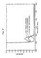
- Each solution was thoroughly stirred and then spin coated on a quartz substrate and baked in an oven at 100°C for one half hour to remove the solvent. The absorbance spectra of the two layers were then measured.
- Figure 1 is a plot of these absorbance characteristics of the two layers and the dye, individually.
- the dye alone curve was obtained by dissolving the dye in chloroform, measuring its absorbance and subtract the chloroform absorbance to get the dye only absorbance.
- the absorbance characteristics of the two layers were indistinguishable except at wavelengths between about 300 and 400 nm.
- the plain polyester had low absorbance in this frequency range, while the dye containing layer had an absorption peak in the vicinity of 350 nm where the dye's own absorption peak is located.
- an IC chip was mounted on a substrate in the manner taught in the above-referenced patents and a Kapton® layer was bonded thereover using the polyester adhesive at a lamination temperature of 150°C.
- a laser at 351 nm was then used to drill holes in the Kapton® polyimide and polyester layers to expose underlying aluminum contact pads.
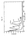
- a polysulfone polymer available under the name Udel from Union Carbide Corporation was used to prepare polymer layers having p-phenylazophenol dye concentrations of 0%, 1% and 2% by weight of the polymer.
- These compositions were formed by dissolving the dye in a solution of the polysulfone in o-dichlorobenzene. Films were formed from these source solutions on quartz in the manner of Example 1 and their absorption spectrum measured. These absorption spectra appear in Figure 2. As can be seen in Figure 2, the dye greatly enhances the absorbance of the Udel at 351 nm.
- thin layers of these compositions were spray coated on aluminum and baked to remove the solvent. The resulting layers were each about 4 microns thick.
- Elvax 410 is a copolymer of ethylene and vinylacetate commercially available for E.I. DuPont de Nemours which has applications as a hot melt adhesive. This material softens well below 100°C and is supplied in pellet form. A formulation was prepared to render this material laser ablatable. 0.4 gram of p-phenylazophenol was mixed at about 120°C with 1 gram of Elvax 410 in the absence of solvents. At this temperature, the copolymer viscosity was low enough to allow uniform mixing and dissolution of the dye. After a few minutes of mixing, the uniform dye/copolymer blend (dyed copolymer) was cooled to room temperature. The dyed copolymer solidified during this cooling.
- the Kapton was laser drilled, but the underlying Elvax layer was unaffected upon microscopic examination.
- the plain ethylene vinylacetate copolymer could not be laser drilled.
- the copolymer sample with 4% dye added was completely laser drilled at power levels as low as 1.5W and 2 scans per hole.
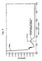
- the extinction coefficient of the azo dye in formulation 2 is larger than the extinction coefficient of the anthroquinone dye in formulation 3.
- sample #1 was laser drilled at power levels as low as 1.2W with 2 scan passes and sample #3 was laser drilled at power levels as low as 1.8W and 2 scan passes.
- the efficiency of the dye additive is directly related to the extinction coefficient and the concentration of dye additive used as is shown by the absorbance of formulation #2 being higher at 351 nm than the absorbance of formulation #3 as shown in Figure 4.
- the dye concentration in the polymer and its depth of penetration into the polymer naturally depends on the dye concentration in the solvent and the length of time allowed for the desired interdiffusion to occur.
- Beneficial dye concentrations may vary from as little as about 0.1% or 1.0% to as much as 10% or more by weight of the source or plain polymer.
- a dye concentration of at least 0.5% is generally needed to significantly increase the laser ablatability of the polymer. While there is in concept no strict upper limit on dye concentration, it is preferred to keep the dye concentration below 10% to minimize effects on the polymer's other properties.
- a dye concentration in the range from 0.5% to 5% is preferred.
- amorphous fluoropolymer family is now commercially available from DuPont De Nemours, Inc. which has desirable characteristics for high density interconnect structures. Two of these products are sold under the trade names teflon AF 1600 and AF 2400. These polymers are amorphous teflon and are soluble in certain perfluorinated solvents. These polymers by themselves have high optical clarity down to 200 nm, however, by addition of the dyes disclosed herein, the polymer can be made laser ablatable at 351 nm. These amorphous fluoropolymers can be readily coated from solution to form dielectric layers for HDI and other structures. The addition of dyes to render these materials laser ablatable makes them fully compatible with the HDI process.
- any of a wide variety of dyes other than p-phenylazophenol, N-p-methoxybenzylidene-p-phenylazoaniline and dihydroxyanthraquinone may be used, either as already formulated, or with substitutions to adjust their absorbance frequencies or newly synthesized dyes may be used.
- These dyes include Sudan III, whose maximum absorbance is at 354 nm, Sudan IV, whose maximum absorbance is at 357 nm, Sudan Orange G, whose maximum absorbance is at 388 nm, Sudan Red 7B, beta carotene, other anthraquinone dyes and so on.
- polystyrene, maleic anhydride copolymers, other polyesters, polycarbonates, vinyl ether copolymers, vinyl acetate polymers and copolymers, polyethersulfones and others may be used.
- a high density interconnect structure 10 incorporating a dielectric layer in accordance with the present invention is illustrated in cross-section in Figure 6 where a substrate 12 has integrated circuit chips 15 disposed in cavities therein.
- the integrated circuits 15 have contact pads 16 disposed on the upper surfaces thereof.
- a Kapton® polyimide layer 20 is bonded to the top of the integrated circuit and the substrate by an adhesive layer 21 of p-phenylazophenol-dye-containing polyester.
- Via holes are laser drilled in the dielectric layers 20/21 and an overlying metal layer 30 is disposed on the top of the dielectric layer and in the via holes and patterned to produce individual conductors 32.
- An additional dielectric layer 40 is disposed over the conductive layer 30 and has via holes 42 disposed therein into which a second metal layer 50 extends to make contact to the first metal layer 30.
- the adhesive layer 21 is a polyester having a melting point in the vicinity of 150°C which is generally considered to be too low a temperature for use in a final product high density interconnect structure in a high temperature environment.
- this structure is ideal for intermediate testing prior to assembly of the final structure since the low melting point of the adhesive 21 facilitates the non-destructive disassembly of the structure at the end of testing, for instance as taught in US-A- entitled “Method and Configuration for Testing Electronic Circuits and Integrated Circuit Chips Using a Removable Overlay Layer" (application Serial No. 230,654 filed August 5, 1988).
- Many other dyes and other polymers may be used in this high density interconnect structure in accordance with this invention.
- the dye be soluble in the polymer with the result that individual molecules of the dye are spaced from each other and substantially evenly distributed in the polymer layer
- this invention can also be successful where the dye is not soluble in the polymer provided it can be distributed substantially uniformly through the polymer as minute particles smaller than about 1 micron in size. Such small particles act very much like individual molecules in transferring their absorbed energy to the host polymer material in order to affect its ablation.
- the dye material may be mixed with the basic polymer at the time of its manufacture with the result that the polymer pellets or powder or the solvent source solution of the polymer, as the case may be, will already incorporate a dye in accordance with this invention.
- This has the advantage of saving the user from the labor and expense of mixing a selected dye with the host polymer in order to provide the desired layer or film.
Applications Claiming Priority (2)
| Application Number | Priority Date | Filing Date | Title |
|---|---|---|---|
| US07/456,421 US5169678A (en) | 1989-12-26 | 1989-12-26 | Laser ablatable polymer dielectrics and methods |
| US456421 | 1989-12-26 |
Publications (1)
| Publication Number | Publication Date |
|---|---|
| EP0436320A2 true EP0436320A2 (fr) | 1991-07-10 |
Family
ID=23812696
Family Applications (1)
| Application Number | Title | Priority Date | Filing Date |
|---|---|---|---|
| EP90313485A Withdrawn EP0436320A2 (fr) | 1989-12-26 | 1990-12-12 | Diélectrique à base de polymÀ¨re attaquable par laser et procédés |
Country Status (3)
| Country | Link |
|---|---|
| US (1) | US5169678A (fr) |
| EP (1) | EP0436320A2 (fr) |
| JP (1) | JP3068213B2 (fr) |
Cited By (12)
| Publication number | Priority date | Publication date | Assignee | Title |
|---|---|---|---|---|
| EP0634695A1 (fr) * | 1993-06-25 | 1995-01-18 | PT Sub, Inc. | Plaque d'impression imagée au laser |
| EP0652486A2 (fr) * | 1993-11-05 | 1995-05-10 | Texas Instruments Incorporated | Production de composantes électroniques et optoélectroniques |
| WO1995017006A1 (fr) * | 1993-12-13 | 1995-06-22 | National Semiconductor Corporation | Procede pour planariser une couche dielectrique d'un circuit integre |
| EP0687009A3 (fr) * | 1994-06-02 | 1996-04-10 | Ibm | Empaquetage multicouche de circuit électronique comprenant des couches polymères diélectriques ayant des pouvoirs d'absorption optique différents et procédé de sa fabrication |
| EP0803769A1 (fr) * | 1996-04-23 | 1997-10-29 | Agfa-Gevaert N.V. | Elément pour l'enregistrement pour la fabrication d'une plaque lithographique avec masque thermosensible incorporé |
| EP0803772A2 (fr) * | 1996-04-23 | 1997-10-29 | Agfa-Gevaert N.V. | Elément formateur d'image et procédé pour la fabrication d'une plaque lithographique avec cet élément |
| EP0803771A1 (fr) * | 1996-04-23 | 1997-10-29 | Agfa-Gevaert N.V. | Méthode pour la fabrication d'une plaque lithographique utilisant un élément formateur d'image contenant un masque thermosensible |
| EP0803770A1 (fr) * | 1996-04-23 | 1997-10-29 | Agfa-Gevaert N.V. | Elément formateur d'images et procédé pour la fabrication d'une plaque lithographique avec cet élément |
| US5879861A (en) * | 1996-04-23 | 1999-03-09 | Agfa-Gevaert, N.V. | Method for making a lithographic printing plate wherein an imaging element is used that comprises a thermosensitive mask |
| US6605410B2 (en) | 1993-06-25 | 2003-08-12 | Polyfibron Technologies, Inc. | Laser imaged printing plates |
| WO2005007735A2 (fr) * | 2003-07-11 | 2005-01-27 | Eastman Chemical Company | Addition d'agents d'absorption d'uv au processus de production de pet pour un rendement maximum |
| US8546723B2 (en) | 2005-09-15 | 2013-10-01 | Plastic Logic Limited | Forming holes using laser energy |
Families Citing this family (58)
| Publication number | Priority date | Publication date | Assignee | Title |
|---|---|---|---|---|
| US5456955A (en) * | 1992-12-11 | 1995-10-10 | Illuminated Display Division Of Bell Industries, Inc. | Method and apparatus for forming an illuminated display |
| US5401687A (en) * | 1993-04-15 | 1995-03-28 | Martin Marietta Corporation | Process for high density interconnection of substrates and integrated circuit chips containing sensitive structures |
| US6916596B2 (en) | 1993-06-25 | 2005-07-12 | Michael Wen-Chein Yang | Laser imaged printing plates |
| US5628926A (en) * | 1993-12-28 | 1997-05-13 | Nec Corporation | Method of forming via holes in a insulation film and method of cutting the insulation film |
| US5449427A (en) * | 1994-05-23 | 1995-09-12 | General Electric Company | Processing low dielectric constant materials for high speed electronics |
| US5527741A (en) * | 1994-10-11 | 1996-06-18 | Martin Marietta Corporation | Fabrication and structures of circuit modules with flexible interconnect layers |
| US5521050A (en) * | 1994-12-16 | 1996-05-28 | Eastman Kodak Company | UV dyes for laser ablative recording process |
| US5561085A (en) | 1994-12-19 | 1996-10-01 | Martin Marietta Corporation | Structure for protecting air bridges on semiconductor chips from damage |
| US5567329A (en) * | 1995-01-27 | 1996-10-22 | Martin Marietta Corporation | Method and system for fabricating a multilayer laminate for a printed wiring board, and a printed wiring board formed thereby |
| US7033648B1 (en) * | 1995-02-06 | 2006-04-25 | International Business Machines Corporations | Means of seeding and metallizing polyimide |
| US5745984A (en) * | 1995-07-10 | 1998-05-05 | Martin Marietta Corporation | Method for making an electronic module |
| US5866952A (en) | 1995-11-30 | 1999-02-02 | Lockheed Martin Corporation | High density interconnected circuit module with a compliant layer as part of a stress-reducing molded substrate |
| US5824374A (en) * | 1996-07-22 | 1998-10-20 | Optical Coating Laboratory, Inc. | In-situ laser patterning of thin film layers during sequential depositing |
| US5932485A (en) * | 1997-10-21 | 1999-08-03 | Micron Technology, Inc. | Method of laser ablation of semiconductor structures |
| GB2338201A (en) * | 1998-06-13 | 1999-12-15 | Exitech Ltd | Laser drilling of holes in materials |
| US5997985A (en) * | 1998-09-10 | 1999-12-07 | Northrop Grumman Corporation | Method of forming acoustic attenuation chambers using laser processing of multi-layered polymer films |
| US6080959A (en) * | 1999-03-12 | 2000-06-27 | Lexmark International, Inc. | System and method for feature compensation of an ablated inkjet nozzle plate |
| US6272271B1 (en) | 1999-04-29 | 2001-08-07 | General Electric Company | Alignment of optical interfaces for data communication |
| WO2001015819A1 (fr) * | 1999-08-30 | 2001-03-08 | Board Of Regents University Of Nebraska-Lincoln | Interconnexions electriques en trois dimensions |
| TWI226814B (en) | 1999-12-16 | 2005-01-11 | Matsushita Electric Ind Co Ltd | A removable film, a substrate with film, a process for forming the removable film and a process for the manufacturing of the circuit board |
| US6624383B1 (en) | 2000-08-30 | 2003-09-23 | Parker-Hannifin Corporation | Using laser etching to improve surface contact resistance of conductive fiber filler polymer composites |
| JP4497262B2 (ja) * | 2000-09-29 | 2010-07-07 | 日本ゼオン株式会社 | 回路基板の製造方法 |
| US6631977B2 (en) | 2001-07-25 | 2003-10-14 | Xerox Corporation | Laser ablatable hydrophobic fluorine-containing graft copolymers |
| US6964881B2 (en) * | 2002-08-27 | 2005-11-15 | Micron Technology, Inc. | Multi-chip wafer level system packages and methods of forming same |
| US6921975B2 (en) * | 2003-04-18 | 2005-07-26 | Freescale Semiconductor, Inc. | Circuit device with at least partial packaging, exposed active surface and a voltage reference plane |
| EP1634673A4 (fr) * | 2003-04-25 | 2009-04-08 | Nitto Denko Corp | Methode de production d'un produit traite par laser et d'une feuille adhesive, pour un traitement laser utilise pour ce produit |
| WO2005057625A2 (fr) * | 2003-12-04 | 2005-06-23 | Matsushita Electric Industrial Co., Ltd. | Procede de formation differentiee de motifs des couches de materiau de film organique mince permettant de ne pas endommager les couches sous-jacentes |
| US20050136333A1 (en) * | 2003-12-19 | 2005-06-23 | Lawrence Brian L. | Novel optical storage materials based on narrowband optical properties |
| JP2005181958A (ja) * | 2003-12-22 | 2005-07-07 | Rohm & Haas Electronic Materials Llc | レーザーアブレーションを用いる電子部品および光学部品の形成方法 |
| WO2005063435A1 (fr) * | 2003-12-25 | 2005-07-14 | Nitto Denko Corporation | Feuille de protection pour traitement laser et procede de production d'un article traite par laser |
| US20070095393A1 (en) * | 2004-03-30 | 2007-05-03 | Piero Zucchelli | Devices and methods for programmable microscale manipulation of fluids |
| JP4854059B2 (ja) * | 2004-07-27 | 2012-01-11 | 日東電工株式会社 | レーザー加工用保護シートを用いたレーザー加工品の製造方法 |
| JP4854061B2 (ja) | 2005-01-14 | 2012-01-11 | 日東電工株式会社 | レーザー加工品の製造方法及びレーザー加工用保護シート |
| JP4873863B2 (ja) * | 2005-01-14 | 2012-02-08 | 日東電工株式会社 | レーザー加工品の製造方法及びレーザー加工用粘着シート |
| US20070031282A1 (en) * | 2005-08-04 | 2007-02-08 | Piero Zucchelli | Devices and methods for interfacing microfluidic devices with fluid handling devices |
| US7262444B2 (en) * | 2005-08-17 | 2007-08-28 | General Electric Company | Power semiconductor packaging method and structure |
| US7829386B2 (en) * | 2005-08-17 | 2010-11-09 | General Electric Company | Power semiconductor packaging method and structure |
| US8497449B1 (en) * | 2006-05-26 | 2013-07-30 | Synchron Laser Service Inc. | Micro-machining of ceramics using an ytterbium fiber-laser |
| EP1975276A1 (fr) * | 2007-03-30 | 2008-10-01 | Danmarks Tekniske Universitet | Préparation d'un article polymère pour une métallisation sélective |
| US20080318413A1 (en) * | 2007-06-21 | 2008-12-25 | General Electric Company | Method for making an interconnect structure and interconnect component recovery process |
| US20080313894A1 (en) * | 2007-06-21 | 2008-12-25 | General Electric Company | Method for making an interconnect structure and low-temperature interconnect component recovery process |
| US9610758B2 (en) * | 2007-06-21 | 2017-04-04 | General Electric Company | Method of making demountable interconnect structure |
| US9953910B2 (en) * | 2007-06-21 | 2018-04-24 | General Electric Company | Demountable interconnect structure |
| US20080318054A1 (en) * | 2007-06-21 | 2008-12-25 | General Electric Company | Low-temperature recoverable electronic component |
| US20080318055A1 (en) * | 2007-06-21 | 2008-12-25 | General Electric Company | Recoverable electronic component |
| US20090028491A1 (en) * | 2007-07-26 | 2009-01-29 | General Electric Company | Interconnect structure |
| US9077206B2 (en) * | 2008-05-14 | 2015-07-07 | National Semiconductor Corporation | Method and system for activating and deactivating an energy generating system |
| US8872062B2 (en) * | 2009-02-03 | 2014-10-28 | Abbott Cardiovascular Systems Inc. | Laser cutting process for forming stents |
| US8530783B2 (en) * | 2009-02-03 | 2013-09-10 | Abbott Cardiovascular Systems Inc. | Laser cutting system |
| EP2393627B1 (fr) * | 2009-02-03 | 2018-05-09 | Abbott Cardiovascular Systems Inc. | Système laser à faisceaux multiples pour former des stents |
| US8556511B2 (en) | 2010-09-08 | 2013-10-15 | Abbott Cardiovascular Systems, Inc. | Fluid bearing to support stent tubing during laser cutting |
| KR102068957B1 (ko) * | 2012-11-28 | 2020-01-22 | 엘지디스플레이 주식회사 | 감광성 유기물질의 절연층을 포함하는 표시장치용 기판 및 그 제조방법 |
| US9566666B2 (en) | 2013-03-13 | 2017-02-14 | Abbott Cardiovascular Systems Inc. | Short pulse laser machining of polymers enhanced with light absorbers for fabricating medical devices |
| US20140299356A1 (en) * | 2013-04-04 | 2014-10-09 | Chong Zhang | Protective film with dye materials for laser absorption enhancement for via drilling |
| US10018912B2 (en) * | 2014-06-13 | 2018-07-10 | Sharp Kabushiki Kaisha | Photosensitive resin composition, wavelength conversion substrate and light emitting device |
| US20160133497A1 (en) * | 2014-11-07 | 2016-05-12 | International Business Machines Corporation | Multi-layer laser debonding structure with tunable absorption |
| US9418895B1 (en) | 2015-03-14 | 2016-08-16 | International Business Machines Corporation | Dies for RFID devices and sensor applications |
| US10780498B2 (en) * | 2018-08-22 | 2020-09-22 | General Electric Company | Porous tools and methods of making the same |
Family Cites Families (6)
| Publication number | Priority date | Publication date | Assignee | Title |
|---|---|---|---|---|
| US4504548A (en) * | 1982-06-25 | 1985-03-12 | Nec Corporation | Optical information recording medium for semiconductor laser |
| US4568632A (en) * | 1982-10-07 | 1986-02-04 | International Business Machines Corporation | Patterning of polyimide films with far ultraviolet light |
| US4547444A (en) * | 1983-12-23 | 1985-10-15 | Minnesota Mining And Manufacturing Company | Recording element for optical data storage |
| US4824699A (en) * | 1987-08-21 | 1989-04-25 | Minnesota Mining And Manufacturing Company | Process for improved adhesion to semicrystalline polymer film |
| US4915981A (en) * | 1988-08-12 | 1990-04-10 | Rogers Corporation | Method of laser drilling fluoropolymer materials |
| US5061341A (en) * | 1990-01-25 | 1991-10-29 | Eastman Kodak Company | Laser-ablating a marking in a coating on plastic articles |
-
1989
- 1989-12-26 US US07/456,421 patent/US5169678A/en not_active Expired - Lifetime
-
1990
- 1990-12-12 EP EP90313485A patent/EP0436320A2/fr not_active Withdrawn
- 1990-12-21 JP JP2412649A patent/JP3068213B2/ja not_active Expired - Fee Related
Cited By (18)
| Publication number | Priority date | Publication date | Assignee | Title |
|---|---|---|---|---|
| US5925500A (en) * | 1993-06-25 | 1999-07-20 | Polyfibron Technologies, Inc. | Method of making laser imaged printing plates utilizing ultraviolet absorbing layer |
| EP0634695A1 (fr) * | 1993-06-25 | 1995-01-18 | PT Sub, Inc. | Plaque d'impression imagée au laser |
| US6756181B2 (en) | 1993-06-25 | 2004-06-29 | Polyfibron Technologies, Inc. | Laser imaged printing plates |
| US6605410B2 (en) | 1993-06-25 | 2003-08-12 | Polyfibron Technologies, Inc. | Laser imaged printing plates |
| EP0652486A2 (fr) * | 1993-11-05 | 1995-05-10 | Texas Instruments Incorporated | Production de composantes électroniques et optoélectroniques |
| EP0652486A3 (fr) * | 1993-11-05 | 1995-12-27 | Texas Instruments Inc | Production de composantes électroniques et optoélectroniques. |
| WO1995017006A1 (fr) * | 1993-12-13 | 1995-06-22 | National Semiconductor Corporation | Procede pour planariser une couche dielectrique d'un circuit integre |
| EP0687009A3 (fr) * | 1994-06-02 | 1996-04-10 | Ibm | Empaquetage multicouche de circuit électronique comprenant des couches polymères diélectriques ayant des pouvoirs d'absorption optique différents et procédé de sa fabrication |
| US5626771A (en) * | 1994-06-02 | 1997-05-06 | International Business Machines Corporation | Design of high density structures with laser etch stop |
| EP0803771A1 (fr) * | 1996-04-23 | 1997-10-29 | Agfa-Gevaert N.V. | Méthode pour la fabrication d'une plaque lithographique utilisant un élément formateur d'image contenant un masque thermosensible |
| EP0803770A1 (fr) * | 1996-04-23 | 1997-10-29 | Agfa-Gevaert N.V. | Elément formateur d'images et procédé pour la fabrication d'une plaque lithographique avec cet élément |
| EP0803772A3 (fr) * | 1996-04-23 | 1997-11-05 | Agfa-Gevaert N.V. | Elément formateur d'image et procédé pour la fabrication d'une plaque lithographique avec cet élément |
| US5879861A (en) * | 1996-04-23 | 1999-03-09 | Agfa-Gevaert, N.V. | Method for making a lithographic printing plate wherein an imaging element is used that comprises a thermosensitive mask |
| EP0803772A2 (fr) * | 1996-04-23 | 1997-10-29 | Agfa-Gevaert N.V. | Elément formateur d'image et procédé pour la fabrication d'une plaque lithographique avec cet élément |
| EP0803769A1 (fr) * | 1996-04-23 | 1997-10-29 | Agfa-Gevaert N.V. | Elément pour l'enregistrement pour la fabrication d'une plaque lithographique avec masque thermosensible incorporé |
| WO2005007735A2 (fr) * | 2003-07-11 | 2005-01-27 | Eastman Chemical Company | Addition d'agents d'absorption d'uv au processus de production de pet pour un rendement maximum |
| WO2005007735A3 (fr) * | 2003-07-11 | 2005-04-14 | Eastman Chem Co | Addition d'agents d'absorption d'uv au processus de production de pet pour un rendement maximum |
| US8546723B2 (en) | 2005-09-15 | 2013-10-01 | Plastic Logic Limited | Forming holes using laser energy |
Also Published As
| Publication number | Publication date |
|---|---|
| US5169678A (en) | 1992-12-08 |
| JP3068213B2 (ja) | 2000-07-24 |
| JPH04120173A (ja) | 1992-04-21 |
Similar Documents
| Publication | Publication Date | Title |
|---|---|---|
| EP0436320A2 (fr) | Diélectrique à base de polymÀ¨re attaquable par laser et procédés | |
| US5040047A (en) | Enhanced fluorescence polymers and interconnect structures using them | |
| EP1484949B1 (fr) | Traitement de matériaux à faible constante diélectrique pour l'électronique à vitesse élevée | |
| US5460921A (en) | High density pattern template: materials and processes for the application of conductive pastes | |
| EP0957664B1 (fr) | Feuille de metal porteuse de resine pour tableau de cablage multicouche, procede de fabrication de cette feuille, tableau de cablage multicouche, et dispositif electronique | |
| KR100270414B1 (ko) | 집적회로 및 그 제조 프로세스 | |
| KR100271487B1 (ko) | 칼라필터용 도너필름 | |
| US5300812A (en) | Plasticized polyetherimide adhesive composition and usage | |
| US5401687A (en) | Process for high density interconnection of substrates and integrated circuit chips containing sensitive structures | |
| US20120276343A1 (en) | Article having closed microchannels | |
| JPH01500974A (ja) | 多重電子回路チップ・パッケージの為に重合体誘電体にバイア孔を作る方法 | |
| MXPA02002381A (es) | Proceso y elemento de transferencia termica con capa de transferencia que contiene plastificante. | |
| JPS61190942A (ja) | 半導体装置の製造に使用するための反射防止膜、この種の反射防止膜の製造方法および製造溶液、並びに紫外線写真平板法にて吸光するための反射防止膜の使用方法 | |
| JP2007099849A (ja) | 樹脂組成物、耐熱性樹脂の製造方法およびそれを用いた電子部品 | |
| JPS61244094A (ja) | 多層配線板の製造方法 | |
| JP2003198100A (ja) | 電気回路を有する基板の製造方法 | |
| JP2021197362A (ja) | 溶融可能および湿潤リンクを有するデバイスの薄膜コーティングパッケージング | |
| JPH0780670A (ja) | レーザによる樹脂膜加工方法 | |
| MXPA95004867A (en) | Processing of low dielectric constant materials for altaveloci electronics | |
| KR20000075833A (ko) | 폴리카보네이트-함유 액상 화학배합물 및 폴리카보네이트 막의제조방법 | |
| KR19980028618A (ko) | 새로운 액정 디스플레이용 칼라필터의 제조방법 | |
| JP2004281657A (ja) | 導電層の形成方法 | |
| DE4332876A1 (de) | Hochwärmebeständige Reliefstrukturen | |
| JPS63165801A (ja) | レ−ザ用光学材料 | |
| JPH11251744A (ja) | 高密度多層プリント基板の作製方法 |
Legal Events
| Date | Code | Title | Description |
|---|---|---|---|
| PUAI | Public reference made under article 153(3) epc to a published international application that has entered the european phase |
Free format text: ORIGINAL CODE: 0009012 |
|
| AK | Designated contracting states |
Kind code of ref document: A2 Designated state(s): DE FR GB IT |
|
| STAA | Information on the status of an ep patent application or granted ep patent |
Free format text: STATUS: THE APPLICATION HAS BEEN WITHDRAWN |
|
| 18W | Application withdrawn |
Withdrawal date: 19920221 |
|
| R18W | Application withdrawn (corrected) |
Effective date: 19920221 |