EP0436282A2 - Procédé de métallisation sélective - Google Patents
Procédé de métallisation sélective Download PDFInfo
- Publication number
- EP0436282A2 EP0436282A2 EP90311953A EP90311953A EP0436282A2 EP 0436282 A2 EP0436282 A2 EP 0436282A2 EP 90311953 A EP90311953 A EP 90311953A EP 90311953 A EP90311953 A EP 90311953A EP 0436282 A2 EP0436282 A2 EP 0436282A2
- Authority
- EP
- European Patent Office
- Prior art keywords
- metal
- plating
- compound
- enabling
- forming
- Prior art date
- Legal status (The legal status is an assumption and is not a legal conclusion. Google has not performed a legal analysis and makes no representation as to the accuracy of the status listed.)
- Withdrawn
Links
Images


Classifications
-
- H—ELECTRICITY
- H10—SEMICONDUCTOR DEVICES; ELECTRIC SOLID-STATE DEVICES NOT OTHERWISE PROVIDED FOR
- H10W—GENERIC PACKAGES, INTERCONNECTIONS, CONNECTORS OR OTHER CONSTRUCTIONAL DETAILS OF DEVICES COVERED BY CLASS H10
- H10W70/00—Package substrates; Interposers; Redistribution layers [RDL]
- H10W70/60—Insulating or insulated package substrates; Interposers; Redistribution layers
- H10W70/611—Insulating or insulated package substrates; Interposers; Redistribution layers for connecting multiple chips together
- H10W70/614—Insulating or insulated package substrates; Interposers; Redistribution layers for connecting multiple chips together the multiple chips being integrally enclosed
-
- C—CHEMISTRY; METALLURGY
- C25—ELECTROLYTIC OR ELECTROPHORETIC PROCESSES; APPARATUS THEREFOR
- C25D—PROCESSES FOR THE ELECTROLYTIC OR ELECTROPHORETIC PRODUCTION OF COATINGS; ELECTROFORMING; APPARATUS THEREFOR
- C25D5/00—Electroplating characterised by the process; Pretreatment or after-treatment of workpieces
- C25D5/02—Electroplating of selected surface areas
- C25D5/022—Electroplating of selected surface areas using masking means
-
- C—CHEMISTRY; METALLURGY
- C25—ELECTROLYTIC OR ELECTROPHORETIC PROCESSES; APPARATUS THEREFOR
- C25D—PROCESSES FOR THE ELECTROLYTIC OR ELECTROPHORETIC PRODUCTION OF COATINGS; ELECTROFORMING; APPARATUS THEREFOR
- C25D5/00—Electroplating characterised by the process; Pretreatment or after-treatment of workpieces
- C25D5/48—After-treatment of electroplated surfaces
- C25D5/50—After-treatment of electroplated surfaces by heat-treatment
-
- C—CHEMISTRY; METALLURGY
- C25—ELECTROLYTIC OR ELECTROPHORETIC PROCESSES; APPARATUS THEREFOR
- C25D—PROCESSES FOR THE ELECTROLYTIC OR ELECTROPHORETIC PRODUCTION OF COATINGS; ELECTROFORMING; APPARATUS THEREFOR
- C25D7/00—Electroplating characterised by the article coated
- C25D7/12—Semiconductors
- C25D7/123—Semiconductors first coated with a seed layer or a conductive layer
-
- H—ELECTRICITY
- H05—ELECTRIC TECHNIQUES NOT OTHERWISE PROVIDED FOR
- H05K—PRINTED CIRCUITS; CASINGS OR CONSTRUCTIONAL DETAILS OF ELECTRIC APPARATUS; MANUFACTURE OF ASSEMBLAGES OF ELECTRICAL COMPONENTS
- H05K3/00—Apparatus or processes for manufacturing printed circuits
- H05K3/10—Apparatus or processes for manufacturing printed circuits in which conductive material is applied to the insulating support in such a manner as to form the desired conductive pattern
- H05K3/108—Apparatus or processes for manufacturing printed circuits in which conductive material is applied to the insulating support in such a manner as to form the desired conductive pattern by semi-additive methods; masks therefor
-
- H—ELECTRICITY
- H10—SEMICONDUCTOR DEVICES; ELECTRIC SOLID-STATE DEVICES NOT OTHERWISE PROVIDED FOR
- H10W—GENERIC PACKAGES, INTERCONNECTIONS, CONNECTORS OR OTHER CONSTRUCTIONAL DETAILS OF DEVICES COVERED BY CLASS H10
- H10W70/00—Package substrates; Interposers; Redistribution layers [RDL]
- H10W70/01—Manufacture or treatment
- H10W70/05—Manufacture or treatment of insulating or insulated package substrates, or of interposers, or of redistribution layers
-
- H—ELECTRICITY
- H05—ELECTRIC TECHNIQUES NOT OTHERWISE PROVIDED FOR
- H05K—PRINTED CIRCUITS; CASINGS OR CONSTRUCTIONAL DETAILS OF ELECTRIC APPARATUS; MANUFACTURE OF ASSEMBLAGES OF ELECTRICAL COMPONENTS
- H05K2203/00—Indexing scheme relating to apparatus or processes for manufacturing printed circuits covered by H05K3/00
- H05K2203/03—Metal processing
- H05K2203/0315—Oxidising metal
-
- H—ELECTRICITY
- H05—ELECTRIC TECHNIQUES NOT OTHERWISE PROVIDED FOR
- H05K—PRINTED CIRCUITS; CASINGS OR CONSTRUCTIONAL DETAILS OF ELECTRIC APPARATUS; MANUFACTURE OF ASSEMBLAGES OF ELECTRICAL COMPONENTS
- H05K2203/00—Indexing scheme relating to apparatus or processes for manufacturing printed circuits covered by H05K3/00
- H05K2203/03—Metal processing
- H05K2203/0361—Stripping a part of an upper metal layer to expose a lower metal layer, e.g. by etching or using a laser
-
- H—ELECTRICITY
- H05—ELECTRIC TECHNIQUES NOT OTHERWISE PROVIDED FOR
- H05K—PRINTED CIRCUITS; CASINGS OR CONSTRUCTIONAL DETAILS OF ELECTRIC APPARATUS; MANUFACTURE OF ASSEMBLAGES OF ELECTRICAL COMPONENTS
- H05K2203/00—Indexing scheme relating to apparatus or processes for manufacturing printed circuits covered by H05K3/00
- H05K2203/10—Using electric, magnetic and electromagnetic fields; Using laser light
- H05K2203/107—Using laser light
-
- H—ELECTRICITY
- H05—ELECTRIC TECHNIQUES NOT OTHERWISE PROVIDED FOR
- H05K—PRINTED CIRCUITS; CASINGS OR CONSTRUCTIONAL DETAILS OF ELECTRIC APPARATUS; MANUFACTURE OF ASSEMBLAGES OF ELECTRICAL COMPONENTS
- H05K3/00—Apparatus or processes for manufacturing printed circuits
- H05K3/38—Improvement of the adhesion between the insulating substrate and the metal
- H05K3/388—Improvement of the adhesion between the insulating substrate and the metal by the use of a metallic or inorganic thin film adhesion layer
Definitions
- the present invention relates to the field of electroplating and microelectronic conductor formation, and more particularly, to selective formation of thick conductive patterns on microelectronic structures and other bodies.
- a high density interconnect (HDI) structure or system which has been developed by General Electric Company offers many advantages in the compact assembly of electronic systems.
- This high density interconnect structure, methods of fabricating it and tools for fabricating it are disclosed in U.S. Patent 4,783,695, entitled “Multichip Integrated Circuit Packaging Configuration and Method" by C.W. Eichelberger, et al.; U.S. Patent 4,835,704, entitled “Adaptive Lithography System to Provide High Density Interconnect” by C.W. Eichelberger, et al.; U.S. Patent 4,714,516, entitled “Method to Produce Via Holes in Polymer Dielectrics for Multiple Electronic Circuit Chip Packaging” by C.W. Eichelberger, et al.; U.S.
- Patent 4,780,177 entitled “Excimer Laser Patterning of a Novel Resist” by R.J. Wojnarowski et al.; U.S. Patent Application Serial No. 249,927, filed September 27, 1988, entitled “Method and Apparatus for Removing Components Bonded to a Substrate” by R.J. Wojnarowski, et al.; U.S. Patent Application Serial No. 310,149 *, filed February 14, 1989, entitled “Laser Beam Scanning Method for Forming Via Holes in Polymer Materials” by C.W. Eichelberger, et al.; U.S. Patent Application Serial No.
- the electronic chips or components of a system are disposed a cavity or cavities of a substrate with their upper surfaces in substantially the same plane as the upper surface of the the rest of the substrate.
- This structure is assembled by providing a thermoplastic adhesive on the bottom of the cavity.
- This thermoplastic adhesive layer may preferably be polyetherimide resin available under the trade name ULTEM® from the General Electric Company.
- the various components are then placed in their desired locations within the cavity, the entire structure is heated to the softening point of the ULTEM® polyetherimide (in the vicinity of 217°C to 235°C depending on the formulation used) and then cooled to thermoplastically bond the individual components to the cavity.
- a polyimide film which may be Kapton® polyimide, available from E.I. du Pont de Nemours Company, which is ⁇ 0.0005-0.003 inch ( ⁇ 12.5-75 microns) thick is pre-treated to promote adhesion and coated on one side with the ULTEM® polyetherimide resin or another thermoplastic and laminated across the top of the chips, other components and the substrate with the ULTEM® resin serving as a thermoplastic adhesive to hold the Kapton® in place.
- via holes are laser drilled in the Kapton® and ULTEM® layers in alignment with contact pads on the electronic components to which it is desired to make contact.
- a metallization layer is deposited over the Kapton® layer.
- This metallization extends into the via holes and makes electrical contact to contact pads disposed at the bottoms thereof.
- a layer of titanium or chromium is normally sputtered directly on top of the dielectric layer to provide good adhesion.
- a layer of copper is then sputtered on the adhesion layer.
- a relatively thick layer of copper is then electroplated on top of the sputtered copper layer to provide a thick, high conductivity conductor. That electroplated copper layer is coated with photoresist which is then laser exposed and developed to provide a mask for etching the copper. The copper is then etched to form a pattern of accurately aligned conductors at the end of the process. Additional dielectric and metallization layers are provided as required in order to provide the desired interconnection pattern. There is a need in this HDI system for a technique which will provide high quality, relatively thick patterned conductor layers in a more efficient manner.
- Electrolytic metal deposition is a widely used industrial process having application to a wide variety of products and fields. In electronic applications where a specific metal pattern is required, electrolytic deposition may be used in either of two manners. In the first, a uniform metal layer is formed by electrolytic deposition, the exposed surface of that layer is coated with a photoresist, the photoresist is then exposed in the desired pattern for the final metal structure, the photoresist is developed and the structure is etched to remove the unprotected electroplated material. In the second technique, a photoresist pattern is disposed on the conductive surface of a substrate structure, exposed and developed to expose the underlying conductive layer in the desired plating pattern.
- the structure is electroplated to produce a thick layer on the exposed portion of the underlying conductive layer.
- these processes both present problems with respect to the durability of the photoresist in the etching or plating bath because extended time periods in these solutions can cause deterioration of the photoresist. Sufficient deterioration of the photoresist results in plating or etching in undesired locations.
- Another technique for plating which can be used for a connected structure is to define the conductor to be plated with photoresist and remove the rest of the layer. This process depends on carrying the plating current through the structure being plated itself.
- Application Serial No. 289,944 discloses a technique which we call selective electrolytic deposition or SED. Selective electrolytic deposition overcomes many of the problems with prior electroplating techniques.
- a body to be plated is provided with an exterior surface which is comprised of two different conductive materials.
- One of these conductive materials forms a plating-preventing compound such as an oxide, while the other does not.
- the metal which does not form the plating-preventing compound is exposed at the surface in the desired plating pattern, while the remainder of the surface is the metal which forms the plating-preventing layer.
- the plating-preventing layer is allowed to form naturally in the case of some oxide plating-preventing compounds such as titanium oxide, chromium oxide and aluminum oxide, respectively on titanium, chromium and aluminum surfaces. In some cases, it is considered desirable to enhance the plating-preventing layer by high temperature oxidation. With other materials, specific processing may be necessary to create a plating-preventing layer.
- the metal on which the plating-preventing layer forms may be disposed on top of the metal on which plating takes place or vice versa. To perform the electroplating, the body is connected to the plating electrode, power turned on and then the body is immersed in the plating bath.
- the portions of the plating-preventing layer and the metal on which it forms which are not covered by the electroplated metal are removed after the electroplating by chemically selective etching as are any underlying metal layers.
- the interdiffusion of the plating-enabling metal may be done either before or after the plating-preventing compound has formed on the surface of the compound-forming metal.
- a number of techniques may be used to selectively interdiffuse the plating-enabling metal.
- a uniform coating of the plating-enabling metal may be formed on the compound-forming metal under conditions in which there is little (preferably no) interdiffusion of the two metals.
- the body is selectively treated in a manner to cause interdiffusion of the metals in those regions where electroplating is desired. This may preferably be done by scanning a laser beam in the desired plating pattern to heat the layer of plating-enabling metal to cause it to interdiffuse with the compound-forming metal.
- the non-interdiffused plating-enabling metal is removed from the body by etching in an etchant for that metal which does not etch the compound-forming metal or which etches it only very slowly.
- the interdiffusion of the plating-preventing metal with the compound-forming metal in the treated areas is sufficient to retain enough of the plating-enabling metal in those locations after etching to ensure that plating will take place in those locations.
- the plating-enabling metal may be provided in the form of an organometallic compound which may be optically, thermally, or otherwise selectively decomposed by appropriate irradiation of the surface of the body in the desired plating pattern in the presence of that organometallic compound.
- This process for depositing the plating-enabling metal may inherently result in the interdiffusion necessary to provide the selective plating.
- additional heating or other treatment may be performed to cause the selectively deposited plating-enabling metal to sufficiently interdiffuse with the compound-forming metal.
- the plating-enabling metal is coated onto a transparent substrate which is placed with the plating-enabling metal layer in contact with or directly adjacent to the body to be selectively plated.
- a laser beam or other appropriate source of energy is then directed through the substrate onto the plating-enabling metal layer to heat it sufficiently to cause evaporation or other transfer of that material onto the body to be plated in a pattern controlled by the pattern of the irradiation of the layer of plating-enabling metal.
- This transfer process itself may produce sufficient interdiffusion to provide selective electrolytic deposition.
- additional heat treatment may be used to cause further interdiffusion of the selectively deposited plating-enabling metal.
- a particularly useful structure which results from this process is one in which spaced apart, conductors are located on a surface of a body. These spaced-apart conductors comprise an electroplated metal disposed on a compound-forming metal which has a plating-enabling metal interdiffused into the surface thereof.
- the electroplated metal can be disposed on the body in a uniform manner, since the plating-enabling metal interdiffusion into the compound-forming metal enables the electroplating of the body which is otherwise not readily electroplatable.
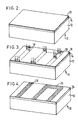
- Figure 1 is a perspective illustration of a substrate 12 on which it is desired to form a patterned layer of electroplated metal.
- the substrate 12 may be electrically insulating or electrically conducting. It may be a uniform body or may have a complex internal structure such as that of an integrated circuit chip or a high density interconnection structure. It may have a substantially planar upper surface as shown, or it may have a surface having substantial topography. The process of this invention is effective with most surface contours.
- the substrate 12 has a layer 14 of a metal which forms a plating-preventing compound (i.e. a layer of a compound-forming metal) disposed on its upper surface.
- the compound-forming metal 14 is a metal which forms a plating-preventing compound under appropriate circumstances as discussed above with reference to application No. 289,944. Titanium, chromium and aluminum are examples of such metals.
- the commonly formed plating-preventing compound is the oxide of the metal which forms as a tight, thin, oxide, dielectric barrier which is effective for preventing electroplating of the compound coated surface of the layer. Other metals and other compounds may also be used.
- a thin layer 16 of a plating-enabling metal is disposed on the upper surface of the compound-forming metal 14.
- the plating-enabling metal 16 is one which (1) does not form a plating-preventing compound under the conditions to which the body 12 will be exposed during the overall process and (2) can be induced to sufficiently interdiffuse into the compound-forming metal that stripping the plating-enabling metal (with an etchant which is selective for the plating-enabling metal as compared to the compound-forming metal) will leave sufficient plating-enabling metal present in the compound-forming metal to enable electroplating of the surface of the interdiffused portion of the compound-forming metal.
- the interdiffused plating-enabling metal defeats the plating-preventing effect of the plating-preventing compound which forms on the surface of the compound-forming metal.
- a preferred plating-enabling metal is gold.
- the plating-enabling metal layer 16 must be deposited in a manner which avoids inducing any significant interdiffusion of the metal 16 into the surface of the metal 14 for reasons discussed briefly above.
- the substrate 12 in combination with the layers 14 and 16 comprise a body 10 which is to be selectively electroplated.
- the body 10 is shown being exposed to actinic radiation in a patterned manner in which the actinic radiation strikes the layer 16 only in those locations which are in alignment with portions of the substrate 12 where electroplating is desired.
- This actinic radiation may be a laser beam, thermal energy, a particle beam or any other radiation which is effective for the purpose.
- the purpose of this exposure is to cause interdiffusion of the plating-enabling metal 16 into the surface of the compound-forming metal in those locations (and only those locations) which are irradiated with the actinic radiation.
- the plating-enabling metal layer is stripped from the body 10 with an etchant which is selective for the plating-enabling metal as opposed to the compound-forming metal.
- the plating-enabling metal 16 is gold
- it is stripped from the body by immersion in aqua regia (a mixture of nitric and hydrochloric acids) to dissolve the non-interdiffused gold everywhere.
- aqua regia a mixture of nitric and hydrochloric acids
- the compound-forming metal 14 has a surface which differs in those areas which were irradiated and those areas which were not. This is shown schematically in Figure 4 by the stippling within the dashed outlines of the regions 20 which were irradiated to cause interdiffusion.
- the exposed surface of the compound-forming metal 14 is substantially pure and has a continuous, pinhole-free oxide coating on it once the body has been exposed to air.
- the plating-enabling metal is interdiffused with the compound-forming metal in a manner which either (1) prevents the formation of the plating-preventing compound or (2) provides a high enough density of pinholes in the surface layer of the plating-preventing compound that good plating contact results and a substantially uniform electroplated layer is formed during the electroplating step. The latter possibility is thought to be what actually occurs.
- Sufficient plating-enabling metal is present in the regions 20 that when the body 10 is connected to the cathode of a copper plating bath, the power turned on and the body immersed in the plating bath, copper electroplates uniformly on the treated regions 20 of the compound-forming metal and not at all on the untreated regions.
- This electroplating is successful even when the body 10 is 2 inches by 2 inches or larger and the only continuous conducting layer in the body 10 through which the plating current can flow is a layer of titanium which is only about 1000 ⁇ thick.
- the body is removed from the plating bath and appears generally as illustrated in Figure 5.
- those portions of the compound-forming metal 14 which are not covered by the electroplated metal are removed by selective chemical etching to produce the structure shown in Figure 6.
- this etching may be done with hydrofluoric acid.
- the quality of the electroplated conductor or line is a function of the degree of laser focus and the quality of the electroplating bath. Using this process, we have plated conductors as narrow as 25 microns wide to a thickness of as much as 4 microns with only slight mushrooming of the plated line as it thickens.
- the body 10, as shown in Figure 2, may be formed in a variety of ways.
- the substrate 12 may be inserted in sputtering apparatus and the layer 14 of the compound-forming metal may be sputtered thereon.
- the substrate 12 and the layer 14 should be cooled prior to and preferably during sputtering of the plating-enabling metal onto the surface of the compound-forming metal in order to ensure that undesired interdiffusion does not take place during the deposition process. Unless such precautions are taken, excessive interdiffusion may occur with the result that uniform plating takes place on the compound-forming metal after stripping of the plating-enabling metal, independent of the selective nature of the patterning interdiffusion step which will be discussed subsequently.
- the plating-enabling metal may be deposited on the compound-forming metal during the same vacuum cycle in which the compound-forming metal was deposited. When that is done, the plating-preventing compound is not present at the interface between the plating-enabling metal 16 and the compound-forming metal 14.
- the vacuum in the sputtering system may be broken and air may be admitted to the sputtering system following the deposition of the compound-forming metal. The vacuum may thereafter be re-established and the plating-enabling metal sputtered onto the now plating-preventing-compound-coated surface of the compound-forming metal 14. Such subsequent deposition may be done in the same sputtering chamber or in a separate sputtering chamber or by other processes.
- the interdiffusion process renders the interdiffused portions 20 of the surface of the compound-forming metal 14 electroplatable.
- the interdiffusion process causes sufficient interdiffusion of the plating-enabling metal through that oxide layer into electrical contact with the underlying compound-forming metal 14 to provide good electroplating contact. More is not required in order to provide selective electrolytic deposition.
- Our work has not shown any difference between (1) test samples in which no oxide was allowed to form prior to the deposition and interdiffusion of gold and (2) test samples where the gold was deposited after formation of an oxide layer on the titanium.
- the gold interdiffusion apparently locally destroys the titanium oxide on at least a microscopic scale, or penetrates the titanium oxide layer in a manner which displaces the oxygen of the titanium oxide in a manner which leaves the gold exposed for electrical contact to the plating bath.
- characteristics of the final body as far as contact resistance between the plated metal and an underlying metal (layer 14) may be affected by such things as the presence of that oxide compound at the interface prior to interdiffusion and the atomic percent in which the plating-enabling metal is present in that surface layer.
- the layer 14 of compound-forming metal which is disposed on the surface of the substrate 12 is the component of the body 10 which interacts in the electroplating process.
- the details of the internal configuration of the substrate 12 are unimportant to the selective electrolytic deposition aspects of the present invention.
- the actual structure of the substrate 12 is quite important, especially if the purpose of the electroplated conductor portions 30 is to provide electrical connections between different portions of the substrate 12, since in that situation, the conductor portions 30 must be properly aligned with respect to the underlying substrate 12 in order to serve their intended purpose.
- interdiffusion as a general term to describe the process of treating the surface of the compound-forming metal 14.
- Other terms which may be used include alloying, diffusion and surface modification.
- the significant feature being the presence of sufficient gold or other plating-enabling metal in the surface of the compound-forming metal to enable electroplating of that surface.
- Our RBS analysis of the gold interdiffused surface of a titanium layer indicates that in the case of gold and titanium, the gold may be present at 1 atomic percent to a depth of as much as 200 ⁇ .
- these two metals are interdiffused such that prior to stripping the gold, there is not a crisp interface at which one could say there is gold only above this point and titanium only below this point.
- the gold etchant aqua regia is incapable of removing that interdiffused gold from the titanium surface. This leads to the selective electrolytic deposition which takes place in this process.
- the process which has just been described involves the deposition of a uniform layer of the plating-enabling metal across the surface of the compound-forming metal, at least in those areas where it is desired to be able to electroplate the body. Obviously, on a body with a large surface, it is only necessary to deposit the plating-enabling metal in the vicinity of regions where plating is desired.
- that plating-enabling metal may be deposited in the precise pattern in which plating is desired and either interdiffused into the compound-forming metal as part of that deposition process, or subsequently, by substantially uniform treatment of the body. Under these circumstances, the patterned nature of the layer of plating-enabling metal controls the locations in which the interdiffusion takes place.
- a combination of selective deposition and selective interdiffusion may be used to provide interdiffusion only in those locations where the plating-enabling metal was deposited and interdiffused.
- a body 10' to be plated comprises a substrate 12 having a uniform layer of a compound-forming metal 14 disposed on the upper surface thereof. Disposed immediately adjacent thereto and preferably in contact therewith, is a plate, a slide or a film 40 comprising a substrate 42 having a uniform layer 46 of the plating-enabling metal disposed thereon.
- the slide 40 is positioned with the plating-enabling metal 46 in direct contact with, or directly adjacent to, the compound-forming metal 14.
- the slide 40 is illustrated slightly displaced from the body 10' in order that the dividing line between the body 10' and the slide 40 will be clear.
- FIG 8 the process of selectively depositing the plating-enabling metal 46 onto the body 10' is illustrated.
- actinic radiation 18 is directed through the transparent substrate 42 onto the layer 46 of plating-enabling metal.
- the actinic radiation is sufficiently intense that the plating-enabling metal 46 is evaporated off the slide 40 and deposited on the upper surface of the compound-forming metal 14 in those locations where the actinic radiation reaches the plating-enabling metal layer.
- the plating-enabling metal may deposit on or may directly interdiffuse into the compound-forming metal 14 to form a selective pattern of the plating-enabling metal 46 on/in the compound-forming metal 14. This is a transfer deposition process, in that the plating-enabling metal is selectively transferred from the slide onto the body to be electroplated.
- the patterning of the actinic radiation 18 may be controlled by a mask 48 as illustrated.
- a laser or other light beam may be scanned across the plate 40 in the desired pattern of the deposition of the plating-enabling metal.
- a substrate 42 of LEXAN® polycarbonate film available from the General Electric Company
- a layer 46 of gold 200 ⁇ thick disposed thereon We used a cw Argon-ion (351nm) laser which was scanned across the film 40 (without a mask) in the desired deposition pattern at a rate of 1.5 mm/sec with a spot size of about 6 microns.
- LEXAN® or another flexible film is a desirable material for use as the transfer substrate because it is flexible and can be wrapped around a curved body or can be held tightly against any body by evacuating the toward-the-body side of the structure to cause air pressure on the away-from-the-body side of the film to cause intimate contact between the gold film and the body for improved resolution in the transfer process.
- Figure 9 the structure of Figures 7 and 8 is illustrated following the transfer process in which the plating enabling layer 46 on the LEXAN® film was ablated off the film in those locations where it was exposed to actinic radiation and formed interdiffused regions 20 on the surface of the compound-forming metal 14 in alignment therewith.
- This body was then electroplated and appeared as shown in Figure 5.
- the electroplated metal 30 deposited only in those locations which had been sensitized or prepared by the plating enabling transfer process.
- the compound forming metal 14 can be removed from this structure in a manner similar to that in the process already described to yield a structure like that in Figure 6.
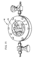
- a body 10 comprises a substrate 12 having a compound-forming metal layer 14 on the surface thereof, is disposed in a reaction chamber 50 ready for the deposition of the plating-enabling metal from a gaseous source material.
- the chamber 50 is formed of stainless steel and has a quartz window.
- the atmosphere in the chamber 50 is controlled by inlet and outlet valves 52 and 54, respectively, and the gas supply and vacuum conditions which are applied thereto.
- a solid source 56 of the gaseous source material is disposed in the chamber 50.
- a sufficient vapor pressure of the source material may be established by heating the entire chamber, or just the source material itself, as may be appropriate under the circumstances when the source material vapor pressure is not sufficient under ambient temperature conditions.
- a laser beam or other energy source is directed at the body 10" in the presence of an appropriate concentration of an organometallic compound of the desired plating-enabling metal in order to deposit the plating-enabling metal in the desired pattern on the body 10".
- suitable organometallic compounds include dimethyl gold-hexafluoroacetylacetonate, dimethyl gold-trifluoroacetylacetonate and dimethyl gold-acetylacetonate.
- Other source compounds may also be used. we prefer the dimethyl hexafluoro compound because of its relatively high vapor pressure. During the decomposition reaction, this source material also releases fluorine which may attack the titanium oxide plating-preventing compound.
- organometallic compounds decompose either thermally or by photoactivation. In either case, focusing a laser beam on the surface of the compound-forming metal 14 on which deposition is desired, results in the deposition of the plating-enabling metal in those locations.
- Two different mechanisms can contribute to this deposition. In the first, the laser heats the surface with the result that molecules of the organometallic compound coming in contact with that portion of the surface are decomposed and leave their metal ions behind on the surface. In the other mechanism, the laser light photodecomposes the organometallic compound with the result that the metal ions deposit on the substrate directly adjacent to the location in which the decomposition takes place.
- the entire body 10" may be heated as shown schematically in Figure 12. This heating may be done in an oven or the body may be treated in another uniform manner to cause further interdiffusion of the plating-enabling metal in those locations where it has already been selectively deposited. Alternatively, the interdiffusion can be done selectively to cause interdiffusion only in those locations where the plating-enabling metal was deposited and which are also selectively treated to cause interdiffusion. Following that interdiffusion step, the body 10" is readied for electroplating to produce the structure illustrated in Figure 5. The background, compound-forming metal may be selectively removed to leave individual electrolytically deposited photoconductors 30 disposed on the substrate 12 as shown in Figure 6.
- the energy delivered to the substrate in the process of thermally or optically decomposing the organometallic compounds produces sufficient interdiffusion of the plating-enabling metal into the compound-forming metal through the plating-preventing compound to produce the desired selective electrolytic deposition upon electroplating.
- plating-enabling metal While each of the specific examples to this point has used gold as the plating-enabling metal, it will be understood that many other metals are potentially suitable, including platinum, palladium, silver and so forth. These metals may be provided as organometallic compounds for metallic deposition. What is required when the plating-enabling metal is deposited on the compound-forming metal without breaking vacuum in a sputtering or other process is that the plating-enabling metal is subsequently sufficiently interdiffused with the compound-forming metal that removal of the bulk of the plating-enabling metal layer in a particular etching or other removal process leaves a sufficient quantity of the plating-enabling metal present only on those portions of the surface which have been "interdiffused" to provide good electroplating contact in those regions while the plating-preventing compound forms on the remainder of the surface of the compound-forming metal. When the plating-preventing compound is already present before deposition of the plating-enabling metal, what is required is sufficient interdiffusion of the plating-enabling metal into the compound-forming metal to provide good electropla
- an electroplated conductor which is disposed on what may be characterized as an adhesion promoting metal (which may be the compound-forming metal) in which a plating enabling or noble-like metal is present in the surface portion of that compound-forming metal in sufficient concentration to provide electroplating contact.
- an adhesion promoting metal which may be the compound-forming metal
- a plating enabling or noble-like metal is present in the surface portion of that compound-forming metal in sufficient concentration to provide electroplating contact.
- Structures which may appear similar which are made by a different process will not contain that typically small percentage of the plating-enabling metal interdiffused in only the surface portion of the compound-forming metal.
- the discussion thus far has focused on selective electroplating of the surface of a body because of the importance of that capability in the microelectronics arts.
- the present invention has much wider applicability in that it provides a means of electroplating metals which form plating-preventing compounds when exposed to air.
- the entire body to be plated can be a compound-forming metal such that the layer 14 is a part of the substrate, rather than a separately formed layer. Titanium, chromium and aluminum are important, common metals which form such plating-preventing compounds which are oxides.
- Diffusing a plating-enabling metal into the surface of such compound-forming metals provides a means of ensuring high quality, uniform electroplating on such metals while eliminating the need for the use of hot, aggressive descaling baths in an attempt to remove surface oxides in a manner which ensures good plating.
- Such aggressive baths are a particular problem when it is desired to plate one of these compound-forming metals which is part of a larger body having portions which would be damaged by the use of normal descaling baths.
- Whether a particular metal is effective as the plating-enabling metal can be easily determined by depositing the potential plating-enabling metal on a substrate having the compound-forming metal as its surface, annealing or otherwise treating the body to ensure that interdiffusion has taken place, stripping the potential plating-enabling metal from the body and electroplating the body. If the electroplating is successful, then the metal being tested is effective as the plating-enabling metal. If no plating takes place, then it is not effective as the plating-enabling metal. Where the metal would be deposited by gas decomposition, such that interdiffusion may not be necessary the metal can be deposited on the test body and the electroplating undertaken to determine its suitability as the plating-enabling metal
Landscapes
- Chemical & Material Sciences (AREA)
- Engineering & Computer Science (AREA)
- Chemical Kinetics & Catalysis (AREA)
- Electrochemistry (AREA)
- Materials Engineering (AREA)
- Metallurgy (AREA)
- Organic Chemistry (AREA)
- Manufacturing & Machinery (AREA)
- Microelectronics & Electronic Packaging (AREA)
- Electroplating Methods And Accessories (AREA)
- Manufacturing Of Printed Wiring (AREA)
- Physical Vapour Deposition (AREA)
Applications Claiming Priority (2)
| Application Number | Priority Date | Filing Date | Title |
|---|---|---|---|
| US459844 | 1990-01-02 | ||
| US07/459,844 US5127998A (en) | 1990-01-02 | 1990-01-02 | Area-selective metallization process |
Publications (1)
| Publication Number | Publication Date |
|---|---|
| EP0436282A2 true EP0436282A2 (fr) | 1991-07-10 |
Family
ID=23826345
Family Applications (1)
| Application Number | Title | Priority Date | Filing Date |
|---|---|---|---|
| EP90311953A Withdrawn EP0436282A2 (fr) | 1990-01-02 | 1990-11-01 | Procédé de métallisation sélective |
Country Status (3)
| Country | Link |
|---|---|
| US (1) | US5127998A (fr) |
| EP (1) | EP0436282A2 (fr) |
| JP (1) | JPH03207886A (fr) |
Cited By (15)
| Publication number | Priority date | Publication date | Assignee | Title |
|---|---|---|---|---|
| US7576369B2 (en) | 2005-10-25 | 2009-08-18 | Udt Sensors, Inc. | Deep diffused thin photodiodes |
| US7656001B2 (en) | 2006-11-01 | 2010-02-02 | Udt Sensors, Inc. | Front-side illuminated, back-side contact double-sided PN-junction photodiode arrays |
| US7655999B2 (en) | 2006-09-15 | 2010-02-02 | Udt Sensors, Inc. | High density photodiodes |
| US7709921B2 (en) | 2008-08-27 | 2010-05-04 | Udt Sensors, Inc. | Photodiode and photodiode array with improved performance characteristics |
| US7880258B2 (en) | 2003-05-05 | 2011-02-01 | Udt Sensors, Inc. | Thin wafer detectors with improved radiation damage and crosstalk characteristics |
| US7898055B2 (en) | 2005-03-16 | 2011-03-01 | Udt Sensors, Inc. | Photodiode with controlled current leakage |
| US8035183B2 (en) | 2003-05-05 | 2011-10-11 | Udt Sensors, Inc. | Photodiodes with PN junction on both front and back sides |
| US8120023B2 (en) | 2006-06-05 | 2012-02-21 | Udt Sensors, Inc. | Low crosstalk, front-side illuminated, back-side contact photodiode array |
| US8324670B2 (en) | 2006-05-15 | 2012-12-04 | Osi Optoelectronics, Inc. | Edge illuminated photodiodes |
| US8399909B2 (en) | 2009-05-12 | 2013-03-19 | Osi Optoelectronics, Inc. | Tetra-lateral position sensing detector |
| US8519503B2 (en) | 2006-06-05 | 2013-08-27 | Osi Optoelectronics, Inc. | High speed backside illuminated, front side contact photodiode array |
| US8686529B2 (en) | 2010-01-19 | 2014-04-01 | Osi Optoelectronics, Inc. | Wavelength sensitive sensor photodiodes |
| US9035412B2 (en) | 2007-05-07 | 2015-05-19 | Osi Optoelectronics, Inc. | Thin active layer fishbone photodiode with a shallow N+ layer and method of manufacturing the same |
| US9178092B2 (en) | 2006-11-01 | 2015-11-03 | Osi Optoelectronics, Inc. | Front-side illuminated, back-side contact double-sided PN-junction photodiode arrays |
| US9691934B2 (en) | 2013-01-24 | 2017-06-27 | Osi Optoelectronics, Inc. | Shallow junction photodiode for detecting short wavelength light |
Families Citing this family (10)
| Publication number | Priority date | Publication date | Assignee | Title |
|---|---|---|---|---|
| US5410179A (en) * | 1990-04-05 | 1995-04-25 | Martin Marietta Corporation | Microwave component having tailored operating characteristics and method of tailoring |
| US5291066A (en) * | 1991-11-14 | 1994-03-01 | General Electric Company | Moisture-proof electrical circuit high density interconnect module and method for making same |
| US5455459A (en) * | 1992-03-27 | 1995-10-03 | Martin Marietta Corporation | Reconstructable interconnect structure for electronic circuits |
| US5561085A (en) | 1994-12-19 | 1996-10-01 | Martin Marietta Corporation | Structure for protecting air bridges on semiconductor chips from damage |
| US5866952A (en) | 1995-11-30 | 1999-02-02 | Lockheed Martin Corporation | High density interconnected circuit module with a compliant layer as part of a stress-reducing molded substrate |
| DE19634488A1 (de) * | 1996-08-26 | 1998-03-05 | Siemens Matsushita Components | Elektro-keramisches Bauelement und Verfahren zu seiner Herstellung |
| US5989994A (en) * | 1998-12-29 | 1999-11-23 | Advantest Corp. | Method for producing contact structures |
| US10197708B2 (en) | 2013-12-19 | 2019-02-05 | Hrl Laboratories, Llc | Structures having selectively metallized regions and methods of manufacturing the same |
| JP7354944B2 (ja) | 2020-07-06 | 2023-10-03 | トヨタ自動車株式会社 | 配線基板の製造方法 |
| JP7456330B2 (ja) | 2020-08-21 | 2024-03-27 | トヨタ自動車株式会社 | 配線基板の製造方法 |
Family Cites Families (6)
| Publication number | Priority date | Publication date | Assignee | Title |
|---|---|---|---|---|
| GB1075634A (en) * | 1963-05-29 | 1967-07-12 | Secr Defence | Electrolytic treatment of titanium surfaces |
| US3708403A (en) * | 1971-09-01 | 1973-01-02 | L Terry | Self-aligning electroplating mask |
| SE7601702L (sv) * | 1975-04-18 | 1976-10-19 | Stauffer Chemical Co | Forfarande for pletering av metaller |
| US4236940A (en) * | 1979-06-12 | 1980-12-02 | United Technologies Corporation | Wear resistant titanium alloy coating |
| FR2476913B1 (fr) * | 1980-02-25 | 1985-09-13 | Nippon Electric Co | Circuit a plusieurs couches pour integration a grande echelle et procede de fabrication de ce circuit |
| US4628149A (en) * | 1981-11-30 | 1986-12-09 | Nippon Electric Co., Ltd. | Substrate having a pattern of an alloy of gold and a noble and a base metal with the pattern isolated by oxides of the noble and the base metals |
-
1990
- 1990-01-02 US US07/459,844 patent/US5127998A/en not_active Expired - Fee Related
- 1990-11-01 EP EP90311953A patent/EP0436282A2/fr not_active Withdrawn
- 1990-11-02 JP JP2295601A patent/JPH03207886A/ja active Pending
Cited By (27)
| Publication number | Priority date | Publication date | Assignee | Title |
|---|---|---|---|---|
| US8035183B2 (en) | 2003-05-05 | 2011-10-11 | Udt Sensors, Inc. | Photodiodes with PN junction on both front and back sides |
| US8907440B2 (en) | 2003-05-05 | 2014-12-09 | Osi Optoelectronics, Inc. | High speed backside illuminated, front side contact photodiode array |
| US7880258B2 (en) | 2003-05-05 | 2011-02-01 | Udt Sensors, Inc. | Thin wafer detectors with improved radiation damage and crosstalk characteristics |
| US7898055B2 (en) | 2005-03-16 | 2011-03-01 | Udt Sensors, Inc. | Photodiode with controlled current leakage |
| US7576369B2 (en) | 2005-10-25 | 2009-08-18 | Udt Sensors, Inc. | Deep diffused thin photodiodes |
| US8324670B2 (en) | 2006-05-15 | 2012-12-04 | Osi Optoelectronics, Inc. | Edge illuminated photodiodes |
| US8120023B2 (en) | 2006-06-05 | 2012-02-21 | Udt Sensors, Inc. | Low crosstalk, front-side illuminated, back-side contact photodiode array |
| US9276022B2 (en) | 2006-06-05 | 2016-03-01 | Osi Optoelectronics, Inc. | Low crosstalk, front-side illuminated, back-side contact photodiode array |
| US8519503B2 (en) | 2006-06-05 | 2013-08-27 | Osi Optoelectronics, Inc. | High speed backside illuminated, front side contact photodiode array |
| US7968964B2 (en) | 2006-09-15 | 2011-06-28 | Osi Optoelectronics, Inc. | High density photodiodes |
| US7655999B2 (en) | 2006-09-15 | 2010-02-02 | Udt Sensors, Inc. | High density photodiodes |
| US8049294B2 (en) | 2006-11-01 | 2011-11-01 | Udt Sensors, Inc. | Front side illuminated, back-side contact double-sided PN-junction photodiode arrays |
| US7656001B2 (en) | 2006-11-01 | 2010-02-02 | Udt Sensors, Inc. | Front-side illuminated, back-side contact double-sided PN-junction photodiode arrays |
| US8278729B2 (en) | 2006-11-01 | 2012-10-02 | Udt Sensors, Inc. | Front-side illuminated, back-side contact double-sided PN-junction photodiode arrays |
| US9178092B2 (en) | 2006-11-01 | 2015-11-03 | Osi Optoelectronics, Inc. | Front-side illuminated, back-side contact double-sided PN-junction photodiode arrays |
| US9035412B2 (en) | 2007-05-07 | 2015-05-19 | Osi Optoelectronics, Inc. | Thin active layer fishbone photodiode with a shallow N+ layer and method of manufacturing the same |
| US7948049B2 (en) | 2008-08-27 | 2011-05-24 | Udt Sensors, Inc. | Photodiode and photodiode array with improved performance characteristics |
| US8816464B2 (en) | 2008-08-27 | 2014-08-26 | Osi Optoelectronics, Inc. | Photodiode and photodiode array with improved performance characteristics |
| US8338905B2 (en) | 2008-08-27 | 2012-12-25 | Osi Optoelectronics, Inc. | Photodiode and photodiode array with improved performance characteristics |
| US7709921B2 (en) | 2008-08-27 | 2010-05-04 | Udt Sensors, Inc. | Photodiode and photodiode array with improved performance characteristics |
| US8698197B2 (en) | 2009-05-12 | 2014-04-15 | Osi Optoelectronics, Inc. | Tetra-lateral position sensing detector |
| US8399909B2 (en) | 2009-05-12 | 2013-03-19 | Osi Optoelectronics, Inc. | Tetra-lateral position sensing detector |
| US9147777B2 (en) | 2009-05-12 | 2015-09-29 | Osi Optoelectronics, Inc. | Tetra-lateral position sensing detector |
| US9577121B2 (en) | 2009-05-12 | 2017-02-21 | Osi Optoelectronics, Inc. | Tetra-lateral position sensing detector |
| US8686529B2 (en) | 2010-01-19 | 2014-04-01 | Osi Optoelectronics, Inc. | Wavelength sensitive sensor photodiodes |
| US9214588B2 (en) | 2010-01-19 | 2015-12-15 | Osi Optoelectronics, Inc. | Wavelength sensitive sensor photodiodes |
| US9691934B2 (en) | 2013-01-24 | 2017-06-27 | Osi Optoelectronics, Inc. | Shallow junction photodiode for detecting short wavelength light |
Also Published As
| Publication number | Publication date |
|---|---|
| US5127998A (en) | 1992-07-07 |
| JPH03207886A (ja) | 1991-09-11 |
Similar Documents
| Publication | Publication Date | Title |
|---|---|---|
| US5127998A (en) | Area-selective metallization process | |
| US5182230A (en) | Laser methods for circuit repair on integrated circuits and substrates | |
| EP0480703B1 (fr) | La formation de configurations de métal sur un substrat | |
| US4349583A (en) | Laser enhanced maskless method for plating and simultaneous plating and etching of patterns | |
| US5292559A (en) | Laser transfer process | |
| JP2683696B2 (ja) | 金属製基層の選択的メッキ法 | |
| US5221426A (en) | Laser etch-back process for forming a metal feature on a non-metal substrate | |
| US5580668A (en) | Aluminum-palladium alloy for initiation of electroless plating | |
| JP3153682B2 (ja) | 回路板の製造方法 | |
| US5167992A (en) | Selective electroless plating process for metal conductors | |
| US4981715A (en) | Method of patterning electroless plated metal on a polymer substrate | |
| EP0787219B1 (fr) | Procede laser de plaquage de traversees | |
| US5084299A (en) | Method for patterning electroless plated metal on a polymer substrate | |
| JPS63105973A (ja) | 光選択的金属付着法 | |
| US4898648A (en) | Method for providing a strengthened conductive circuit pattern | |
| US5230965A (en) | High density interconnect with electroplated conductors | |
| US5192581A (en) | Protective layer for preventing electroless deposition on a dielectric | |
| US4711822A (en) | Metal core printed circuit boards | |
| US5171709A (en) | Laser methods for circuit repair on integrated circuits and substrates | |
| US4909895A (en) | System and method for providing a conductive circuit pattern utilizing thermal oxidation | |
| EP0536376A1 (fr) | Procede de preparation d'une couche d'activation pour effectuer un depot de metal selectif. | |
| KR19980018163A (ko) | 유기 전자 패키지 및 이에 팔라듐-주석 씨드층을 도포하는 방법 | |
| JP2008524871A (ja) | フレキシブル回路およびその製造方法 | |
| KR20230028238A (ko) | 배선 구조체 및 그 제조 방법, 및 반도체 패키지 | |
| JPH04109510A (ja) | 異方導電膜の製造方法 |
Legal Events
| Date | Code | Title | Description |
|---|---|---|---|
| PUAI | Public reference made under article 153(3) epc to a published international application that has entered the european phase |
Free format text: ORIGINAL CODE: 0009012 |
|
| AK | Designated contracting states |
Kind code of ref document: A2 Designated state(s): DE FR GB IT |
|
| STAA | Information on the status of an ep patent application or granted ep patent |
Free format text: STATUS: THE APPLICATION HAS BEEN WITHDRAWN |
|
| 18W | Application withdrawn |
Withdrawal date: 19920221 |
|
| R18W | Application withdrawn (corrected) |
Effective date: 19920221 |