EP0436211A2 - Verfahren und Vorrichtung zur Beobachtung interner speicherzugeodneter Register - Google Patents
Verfahren und Vorrichtung zur Beobachtung interner speicherzugeodneter Register Download PDFInfo
- Publication number
- EP0436211A2 EP0436211A2 EP90125335A EP90125335A EP0436211A2 EP 0436211 A2 EP0436211 A2 EP 0436211A2 EP 90125335 A EP90125335 A EP 90125335A EP 90125335 A EP90125335 A EP 90125335A EP 0436211 A2 EP0436211 A2 EP 0436211A2
- Authority
- EP
- European Patent Office
- Prior art keywords
- registers
- bus
- external
- cpu
- data
- Prior art date
- Legal status (The legal status is an assumption and is not a legal conclusion. Google has not performed a legal analysis and makes no representation as to the accuracy of the status listed.)
- Granted
Links
Images
Classifications
-
- G—PHYSICS
- G06—COMPUTING OR CALCULATING; COUNTING
- G06F—ELECTRIC DIGITAL DATA PROCESSING
- G06F12/00—Accessing, addressing or allocating within memory systems or architectures
- G06F12/02—Addressing or allocation; Relocation
- G06F12/06—Addressing a physical block of locations, e.g. base addressing, module addressing, memory dedication
-
- G—PHYSICS
- G06—COMPUTING OR CALCULATING; COUNTING
- G06F—ELECTRIC DIGITAL DATA PROCESSING
- G06F11/00—Error detection; Error correction; Monitoring
- G06F11/36—Prevention of errors by analysis, debugging or testing of software
- G06F11/362—Debugging of software
- G06F11/3648—Debugging of software using additional hardware
- G06F11/3656—Debugging of software using additional hardware using a specific debug interface
-
- G—PHYSICS
- G06—COMPUTING OR CALCULATING; COUNTING
- G06F—ELECTRIC DIGITAL DATA PROCESSING
- G06F13/00—Interconnection of, or transfer of information or other signals between, memories, input/output devices or central processing units
-
- G—PHYSICS
- G06—COMPUTING OR CALCULATING; COUNTING
- G06F—ELECTRIC DIGITAL DATA PROCESSING
- G06F13/00—Interconnection of, or transfer of information or other signals between, memories, input/output devices or central processing units
- G06F13/10—Program control for peripheral devices
- G06F13/12—Program control for peripheral devices using hardware independent of the central processor, e.g. channel or peripheral processor
Definitions
- the present invention relates to data processing systems, and more specifically to a method and apparatus for observing the contents of a central processing unit's internal memory-mapped registers.
- the central processing unit In conventional digital data processing system with n-bit architecture, the central processing unit (CPU) is capable of generating 2 n addresses for referencing instructions or data. For example, a 16-bit computer is capable of generating 216 or 65,536 addresses. These addresses are generally used to reference devices which are located outside the CPU environment, so-called peripheral or external devices.
- the interface between the CPU and the peripheral devices consists of a system bus, including an address bus and a data bus, wherein the CPU, responding to an instruction request, sends an address onto the address bus which is connected to the peripheral device.
- the peripheral device is memory storage, then data can be transferred directly between the CPU and memory by means of the data bus. If, however, the peripheral device is something other than a memory device, such as a printer, modem, or a co-processor, then additional hardware is generally required in the peripheral device in order to decode and act on the address reference.
- a technique called "memory-mapped I/O" is used. According to this technique, the transfer of data to and from peripheral devices is accomplished by using some of the normally available memory space. Memory addresses are decoded within the peripheral device and thus are used to determine when a specific device is being addressed. Usually, each type of function within the peripheral device is assigned a memory address and may then be accessed by the CPU. For example, the status, control and data registers within the peripheral devices are each assigned a memory address and thus three addresses are required for the CPU to perform an I/O operation with this peripheral device. Using memory-mapped I/O in this fashion allows I/O operations to be performed directly in a high-level language, i.e., an I/O device may be declared as a data structure and then manipulated with the use of pointers.
- the sequence of events occurring during a basic CPU access to either memory or peripheral device for a read transaction or a write transaction is performed in two cycles of a bus clock, the cycles commonly being labeled T1 and T2.
- the CPU asserts an Address Strobe signal ADS which indicates that a bus cycle has begun and that a valid address is on the Address Bus. From the beginning of cycle T1 until the completion of the bus cycle, the CPU drives the Address Bus and other relevant control signals. If the bus cycle is not cancelled (e.g. cycle T2 is entered in the next clock cycle), the CPU will assert a Confirm signal CONF in the middle of cycle T1 to indicate that the bus cycle initiated by the Address Strobe ADS is valid.
- a confirmed bus cycle is completed at the end of cycle T2.
- the CPU samples the Data Bus at the end of cycle T2. If a bus exception is detected, then data on the Data Bus is ignored. For write operations, valid data is output on the Data Bus to the address indicated on the Address Bus from the middle of cycle T1 until the end of the cycle.
- Some systems e.g., the Intel 80186 microprocessor, solve the problem by showing accesses to internal memory-mapped registers as normal read/write cycles, as described above. However, the CPU ignores the synchronous and asynchronous ready bits as well as the data bus, thus the data contained in the internal memory-mapped registers can not be observed.
- the present invention as defined in claims 1 and 4, in brief provides a microprocessor architecture which allows the contents of internal memory-mapped registers to be observed. This is achieved by adding a new CPU output signal to the conventional architecture which indicates that an internal bus cycle is underway, deactivating the CPU output signal which validates an external reference cycle and then accessing the contents of the internal memory-mapped registers and placing the information contained therein on the data bus for observation.
- the present invention will thus aid system programmers by allowing them to trace program activity with the internal registers of the CPU, an invaluable debugging tool. This will further facilitate the integration of controllers and co-processors on-chip since system designers will now be able to troubleshoot internal problems associated with integration.
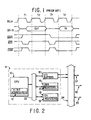
- Fig.1 is a timing diagram illustrating a read and write cycle of a conventional microprocessor.
- Fig.2 is a block diagram illustrating a typical microprocessor chip with integrated controllers.
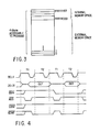
- Fig.3 is a block diagram illustrating memory allocation of a microprocessor which utilizes memory-mapped addressing.
- Fig.4 is a timing diagram illustrating internal read and write cycles of a microprocessor in accord with the present invention.
- Fig.2 shows a general block diagram of a microprocessor (CPU) 10 with Direct Memory Access (DMA) 16 and Interrupt Control Unit (ICU) 18 integrated on chip 11.
- the DMA 16 and ICU 18 are interfaced with the CPU 10 by means of an internal bus 22.
- User interface to the DMA 16 and ICU 18 is provided via the I/O buffers 15 on the system bus 34, which includes a Data Bus 35, an Address Bus 36 and I/O pins 37.
- the CPU 10 is capable of addressing 2 N locations, where N is the number of bits in the CPU's address field 12.
- the memory of the CPU 10 is organized as a set of linear addresses beginning at 0 and ending at N-1. A portion of these memory addresses are dedicated for memory-mapping.
- 232 (4 gigabytes) of linear address space can be referenced and these addresses are numbered sequentially starting at zero and ending at 232-1.
- the hex addresses in the range FFFFF000 to FFFFFFFF are dedicated to on-chip ("internal") memory-mapped registers.
- the DMA 16 and ICU 18 each have Control and Status Registers 17 and 19, respectively, which are referenced as memory-mapped registers.
- the basic CPU operation to read from and write to external memory and peripheral devices consists of activating a first output signal to indicate that a bus cycle has begun and that there is a valid address on the Address Bus 36. Next, if the bus cycle is not cancelled, a second output signal is asserted which qualifies access to the peripheral by confirming that a valid bus cycle is underway. Lastly, access to the peripheral is gained and the data is presented on the Data Bus 35, the direction of data transfer depending on the value of a third output signal. For example, referring to Fig. 1, in the National Semiconductor NS-32532 microprocessor, the basic bus cycles occur during two cycles (T1 and T2) of the Bus Clock BCLK.
- the CPU asserts Address Strobe signal ADS during the first half of cycle T1 to indicate the beginning of a bus cycle.
- the CPU asserts a Confirm Bus Cycle signal CONF to allow external access, CONF being active from the middle of cycle T1 until the completion of the bus cycle, at which time CONF is negated.
- Data transfer may then take place and be observed on the Data Bus 35.
- the direction of transfer is indicated by output signal Data Direction DDIN , i.e., write when DDIN is high and read when DDIN is low.
- the normal read/write cycle may be modified by deactivating the output signal which allows external access and by asserting a fourth output signal which indicates that access to internal memory-mapped registers 17 and 19 will take place.
- the contents of the internal registers 17 and 19 may then be observed on the Data Bus 35.
- CONF is held inactive, thus disabling external memory access.
- a new output signal, Confirm Internal Bus Cycle ICONF is then asserted indicating internal access is requested and bus control inputs should be ignored.
- Data is presented on the Data Bus 35. Note however, that on internal read cycles, DDIN is low, but the data direction is the same as in a write cycle.
Landscapes
- Engineering & Computer Science (AREA)
- Theoretical Computer Science (AREA)
- Physics & Mathematics (AREA)
- General Engineering & Computer Science (AREA)
- General Physics & Mathematics (AREA)
- Computer Hardware Design (AREA)
- Quality & Reliability (AREA)
- Debugging And Monitoring (AREA)
Applications Claiming Priority (2)
| Application Number | Priority Date | Filing Date | Title |
|---|---|---|---|
| US46102390A | 1990-01-04 | 1990-01-04 | |
| US461023 | 1999-12-15 |
Publications (3)
| Publication Number | Publication Date |
|---|---|
| EP0436211A2 true EP0436211A2 (de) | 1991-07-10 |
| EP0436211A3 EP0436211A3 (en) | 1992-03-18 |
| EP0436211B1 EP0436211B1 (de) | 2001-07-11 |
Family
ID=23830931
Family Applications (1)
| Application Number | Title | Priority Date | Filing Date |
|---|---|---|---|
| EP90125335A Expired - Lifetime EP0436211B1 (de) | 1990-01-04 | 1990-12-22 | Vorrichtung die die Beobachtung interner speicherzugeordneten Register ermöglicht |
Country Status (4)
| Country | Link |
|---|---|
| EP (1) | EP0436211B1 (de) |
| JP (1) | JPH0773132A (de) |
| KR (1) | KR100223096B1 (de) |
| DE (1) | DE69033759T2 (de) |
Cited By (5)
| Publication number | Priority date | Publication date | Assignee | Title |
|---|---|---|---|---|
| EP0628909A3 (de) * | 1993-06-11 | 1996-01-24 | Nec Corp | Programm zur Ablaufverfolgung und Verfahren zur Ablaufverfolgung. |
| WO1998007091A1 (en) * | 1996-08-14 | 1998-02-19 | Advanced Micro Devices, Inc. | A microcontroller configured to convey data corresponding to internal memory accesses externally |
| US5860161A (en) * | 1996-08-14 | 1999-01-12 | Advanced Micro Devices, Inc. | Microcontroller configured to indicate internal memory accesses externally |
| US5862148A (en) * | 1997-02-11 | 1999-01-19 | Advanced Micro Devices, Inc. | Microcontroller with improved debug capability for internal memory |
| EP1089182A2 (de) * | 1999-10-01 | 2001-04-04 | STMicroelectronics, Inc. | System und Verfahren zur Übertragung mit einer integrierten Schaltung |
Family Cites Families (2)
| Publication number | Priority date | Publication date | Assignee | Title |
|---|---|---|---|---|
| US4674089A (en) * | 1985-04-16 | 1987-06-16 | Intel Corporation | In-circuit emulator |
| US5084814A (en) * | 1987-10-30 | 1992-01-28 | Motorola, Inc. | Data processor with development support features |
-
1990
- 1990-12-22 EP EP90125335A patent/EP0436211B1/de not_active Expired - Lifetime
- 1990-12-22 DE DE69033759T patent/DE69033759T2/de not_active Expired - Lifetime
- 1990-12-28 JP JP2418536A patent/JPH0773132A/ja active Pending
- 1990-12-29 KR KR1019900022362A patent/KR100223096B1/ko not_active Expired - Lifetime
Cited By (6)
| Publication number | Priority date | Publication date | Assignee | Title |
|---|---|---|---|---|
| EP0628909A3 (de) * | 1993-06-11 | 1996-01-24 | Nec Corp | Programm zur Ablaufverfolgung und Verfahren zur Ablaufverfolgung. |
| WO1998007091A1 (en) * | 1996-08-14 | 1998-02-19 | Advanced Micro Devices, Inc. | A microcontroller configured to convey data corresponding to internal memory accesses externally |
| US5860161A (en) * | 1996-08-14 | 1999-01-12 | Advanced Micro Devices, Inc. | Microcontroller configured to indicate internal memory accesses externally |
| US5903912A (en) * | 1996-08-14 | 1999-05-11 | Advanced Micro Devices, Inc. | Microcontroller configured to convey data corresponding to internal memory accesses externally |
| US5862148A (en) * | 1997-02-11 | 1999-01-19 | Advanced Micro Devices, Inc. | Microcontroller with improved debug capability for internal memory |
| EP1089182A2 (de) * | 1999-10-01 | 2001-04-04 | STMicroelectronics, Inc. | System und Verfahren zur Übertragung mit einer integrierten Schaltung |
Also Published As
| Publication number | Publication date |
|---|---|
| DE69033759T2 (de) | 2002-05-08 |
| DE69033759D1 (de) | 2001-08-16 |
| KR100223096B1 (ko) | 1999-10-15 |
| EP0436211A3 (en) | 1992-03-18 |
| JPH0773132A (ja) | 1995-03-17 |
| EP0436211B1 (de) | 2001-07-11 |
| KR910014812A (ko) | 1991-08-31 |
Similar Documents
| Publication | Publication Date | Title |
|---|---|---|
| KR0168656B1 (ko) | 데이터 처리 시스템 | |
| US5640542A (en) | On-chip in-circuit-emulator memory mapping and breakpoint register modules | |
| US5664199A (en) | Microcomputer free from control of central processing unit (CPU) for receiving and writing instructions into memory independent of and during execution of CPU | |
| US5577230A (en) | Apparatus and method for computer processing using an enhanced Harvard architecture utilizing dual memory buses and the arbitration for data/instruction fetch | |
| EP0523764A2 (de) | Rechnersystem mit Direktbusanschluss zwischen dem Prozessor und dem dynamischen Datenspeicher und mit einer im Prozessor aufgenommenen DMA-Steuerung in Bezug auf eine Anzahl von Datenaustauschmitteln ebenfalls im Anschluss an den Bus und Zentralprozessor zur Verwendung in einem derartigen Rechnersystem | |
| US6205509B1 (en) | Method for improving interrupt response time | |
| US6484273B1 (en) | Integrated EJTAG external bus interface | |
| US6092219A (en) | Method for use of bus parking states to communicate diagnostic information | |
| US5379402A (en) | Data processing device for preventing inconsistency of data stored in main memory and cache memory | |
| US5574937A (en) | Method and apparatus for improving instruction tracing operations in a computer system | |
| US5900014A (en) | External means of overriding and controlling cacheability attribute of selected CPU accesses to monitor instruction and data streams | |
| US5212775A (en) | Method and apparatus for observing internal memory-mapped registers | |
| US5933613A (en) | Computer system and inter-bus control circuit | |
| EP0676687B1 (de) | Stromverwaltungseinheiten für Rechnersysteme | |
| EP0436211B1 (de) | Vorrichtung die die Beobachtung interner speicherzugeordneten Register ermöglicht | |
| KR920002830B1 (ko) | 다이렉트 메모리 액세스 제어장치 | |
| JP3323341B2 (ja) | エミュレーション用プロセッサおよびそれを搭載したエミュレータ | |
| US20040221212A1 (en) | Digital signal processor including an interface therein capable of allowing direct access to registers from an external device | |
| US6282600B1 (en) | Method and apparatus of resolving conflicting register access requests from a service processor and system processor | |
| JPS59197946A (ja) | メモリ装置 | |
| JPH0581087A (ja) | プロセサのモニタ方式 | |
| JP2520158B2 (ja) | ディジタルシグナルプロセッサのデバッグ方式 | |
| JP3199138B2 (ja) | マイクロプロセッサ | |
| JPS6215644A (ja) | キヤツシユメモリ制御回路 | |
| JPH0324640A (ja) | 情報処理装置のデバッグ方式 |
Legal Events
| Date | Code | Title | Description |
|---|---|---|---|
| PUAI | Public reference made under article 153(3) epc to a published international application that has entered the european phase |
Free format text: ORIGINAL CODE: 0009012 |
|
| AK | Designated contracting states |
Kind code of ref document: A2 Designated state(s): DE FR GB IT |
|
| PUAL | Search report despatched |
Free format text: ORIGINAL CODE: 0009013 |
|
| AK | Designated contracting states |
Kind code of ref document: A3 Designated state(s): DE FR GB IT |
|
| 17P | Request for examination filed |
Effective date: 19920723 |
|
| 17Q | First examination report despatched |
Effective date: 19950201 |
|
| RTI1 | Title (correction) |
Free format text: APPARATUS ENABLING OBSERVATION OF INTERNAL MEMORY-MAPPED REGISTERS |
|
| GRAG | Despatch of communication of intention to grant |
Free format text: ORIGINAL CODE: EPIDOS AGRA |
|
| GRAG | Despatch of communication of intention to grant |
Free format text: ORIGINAL CODE: EPIDOS AGRA |
|
| GRAH | Despatch of communication of intention to grant a patent |
Free format text: ORIGINAL CODE: EPIDOS IGRA |
|
| GRAH | Despatch of communication of intention to grant a patent |
Free format text: ORIGINAL CODE: EPIDOS IGRA |
|
| GRAA | (expected) grant |
Free format text: ORIGINAL CODE: 0009210 |
|
| AK | Designated contracting states |
Kind code of ref document: B1 Designated state(s): DE FR GB IT |
|
| PG25 | Lapsed in a contracting state [announced via postgrant information from national office to epo] |
Ref country code: IT Free format text: LAPSE BECAUSE OF FAILURE TO SUBMIT A TRANSLATION OF THE DESCRIPTION OR TO PAY THE FEE WITHIN THE PRE;WARNING: LAPSES OF ITALIAN PATENTS WITH EFFECTIVE DATE BEFORE 2007 MAY HAVE OCCURRED AT ANY TIME BEFORE 2007. THE CORRECT EFFECTIVE DATE MAY BE DIFFERENT FROM THE ONE RECORDED.SCRIBED TIME-LIMIT Effective date: 20010711 Ref country code: FR Free format text: LAPSE BECAUSE OF FAILURE TO SUBMIT A TRANSLATION OF THE DESCRIPTION OR TO PAY THE FEE WITHIN THE PRESCRIBED TIME-LIMIT Effective date: 20010711 |
|
| REF | Corresponds to: |
Ref document number: 69033759 Country of ref document: DE Date of ref document: 20010816 |
|
| EN | Fr: translation not filed | ||
| PG25 | Lapsed in a contracting state [announced via postgrant information from national office to epo] |
Ref country code: GB Free format text: LAPSE BECAUSE OF NON-PAYMENT OF DUE FEES Effective date: 20011222 |
|
| REG | Reference to a national code |
Ref country code: GB Ref legal event code: IF02 |
|
| PLBE | No opposition filed within time limit |
Free format text: ORIGINAL CODE: 0009261 |
|
| STAA | Information on the status of an ep patent application or granted ep patent |
Free format text: STATUS: NO OPPOSITION FILED WITHIN TIME LIMIT |
|
| 26N | No opposition filed | ||
| GBPC | Gb: european patent ceased through non-payment of renewal fee |
Effective date: 20011222 |
|
| PGFP | Annual fee paid to national office [announced via postgrant information from national office to epo] |
Ref country code: DE Payment date: 20091028 Year of fee payment: 20 |
|
| PG25 | Lapsed in a contracting state [announced via postgrant information from national office to epo] |
Ref country code: DE Free format text: LAPSE BECAUSE OF EXPIRATION OF PROTECTION Effective date: 20101222 |