EP0436070A1 - Appareillage et procédé de depôt chimique en phase vapeur pour la production d'une couche mince - Google Patents
Appareillage et procédé de depôt chimique en phase vapeur pour la production d'une couche mince Download PDFInfo
- Publication number
- EP0436070A1 EP0436070A1 EP90116005A EP90116005A EP0436070A1 EP 0436070 A1 EP0436070 A1 EP 0436070A1 EP 90116005 A EP90116005 A EP 90116005A EP 90116005 A EP90116005 A EP 90116005A EP 0436070 A1 EP0436070 A1 EP 0436070A1
- Authority
- EP
- European Patent Office
- Prior art keywords
- substrate
- temperature
- power supply
- heating
- cooling
- Prior art date
- Legal status (The legal status is an assumption and is not a legal conclusion. Google has not performed a legal analysis and makes no representation as to the accuracy of the status listed.)
- Granted
Links
- 238000000034 method Methods 0.000 title claims abstract description 27
- 239000010409 thin film Substances 0.000 title claims abstract description 22
- 238000005229 chemical vapour deposition Methods 0.000 title claims abstract description 11
- 239000000758 substrate Substances 0.000 claims abstract description 143
- 238000001816 cooling Methods 0.000 claims abstract description 34
- 238000010438 heat treatment Methods 0.000 claims abstract description 34
- 239000010432 diamond Substances 0.000 claims abstract description 27
- 229910003460 diamond Inorganic materials 0.000 claims abstract description 26
- 230000008569 process Effects 0.000 claims abstract description 9
- 238000000151 deposition Methods 0.000 claims description 20
- 230000008021 deposition Effects 0.000 claims description 14
- 239000010408 film Substances 0.000 claims description 11
- 230000004044 response Effects 0.000 claims description 4
- XLYOFNOQVPJJNP-UHFFFAOYSA-N water Substances O XLYOFNOQVPJJNP-UHFFFAOYSA-N 0.000 claims 1
- 238000006243 chemical reaction Methods 0.000 abstract description 14
- 239000013078 crystal Substances 0.000 abstract description 6
- 239000007789 gas Substances 0.000 description 22
- 239000000498 cooling water Substances 0.000 description 9
- 230000005855 radiation Effects 0.000 description 7
- VNWKTOKETHGBQD-UHFFFAOYSA-N methane Chemical compound C VNWKTOKETHGBQD-UHFFFAOYSA-N 0.000 description 6
- 238000005268 plasma chemical vapour deposition Methods 0.000 description 6
- VYPSYNLAJGMNEJ-UHFFFAOYSA-N Silicium dioxide Chemical compound O=[Si]=O VYPSYNLAJGMNEJ-UHFFFAOYSA-N 0.000 description 5
- XUIMIQQOPSSXEZ-UHFFFAOYSA-N Silicon Chemical compound [Si] XUIMIQQOPSSXEZ-UHFFFAOYSA-N 0.000 description 5
- 238000005259 measurement Methods 0.000 description 5
- 229910052710 silicon Inorganic materials 0.000 description 5
- 239000010703 silicon Substances 0.000 description 5
- 238000004050 hot filament vapor deposition Methods 0.000 description 4
- 235000012239 silicon dioxide Nutrition 0.000 description 4
- 238000001069 Raman spectroscopy Methods 0.000 description 3
- 239000000463 material Substances 0.000 description 3
- 238000005240 physical vapour deposition Methods 0.000 description 3
- 239000010453 quartz Substances 0.000 description 3
- 238000010183 spectrum analysis Methods 0.000 description 3
- OKTJSMMVPCPJKN-UHFFFAOYSA-N Carbon Chemical compound [C] OKTJSMMVPCPJKN-UHFFFAOYSA-N 0.000 description 2
- RYGMFSIKBFXOCR-UHFFFAOYSA-N Copper Chemical compound [Cu] RYGMFSIKBFXOCR-UHFFFAOYSA-N 0.000 description 2
- UFHFLCQGNIYNRP-UHFFFAOYSA-N Hydrogen Chemical compound [H][H] UFHFLCQGNIYNRP-UHFFFAOYSA-N 0.000 description 2
- 229910052799 carbon Inorganic materials 0.000 description 2
- 230000008859 change Effects 0.000 description 2
- 229910052802 copper Inorganic materials 0.000 description 2
- 239000010949 copper Substances 0.000 description 2
- PMHQVHHXPFUNSP-UHFFFAOYSA-M copper(1+);methylsulfanylmethane;bromide Chemical compound Br[Cu].CSC PMHQVHHXPFUNSP-UHFFFAOYSA-M 0.000 description 2
- 229910052739 hydrogen Inorganic materials 0.000 description 2
- 239000001257 hydrogen Substances 0.000 description 2
- 239000011810 insulating material Substances 0.000 description 2
- 229910052751 metal Inorganic materials 0.000 description 2
- 239000002184 metal Substances 0.000 description 2
- 238000007740 vapor deposition Methods 0.000 description 2
- 229910052582 BN Inorganic materials 0.000 description 1
- PZNSFCLAULLKQX-UHFFFAOYSA-N Boron nitride Chemical compound N#B PZNSFCLAULLKQX-UHFFFAOYSA-N 0.000 description 1
- 229910052581 Si3N4 Inorganic materials 0.000 description 1
- BQCADISMDOOEFD-UHFFFAOYSA-N Silver Chemical compound [Ag] BQCADISMDOOEFD-UHFFFAOYSA-N 0.000 description 1
- PNEYBMLMFCGWSK-UHFFFAOYSA-N aluminium oxide Inorganic materials [O-2].[O-2].[O-2].[Al+3].[Al+3] PNEYBMLMFCGWSK-UHFFFAOYSA-N 0.000 description 1
- 238000009529 body temperature measurement Methods 0.000 description 1
- 238000009835 boiling Methods 0.000 description 1
- 238000005219 brazing Methods 0.000 description 1
- 238000002485 combustion reaction Methods 0.000 description 1
- 239000002131 composite material Substances 0.000 description 1
- 239000004020 conductor Substances 0.000 description 1
- 239000002826 coolant Substances 0.000 description 1
- 230000003247 decreasing effect Effects 0.000 description 1
- 238000010586 diagram Methods 0.000 description 1
- 238000010292 electrical insulation Methods 0.000 description 1
- 150000002431 hydrogen Chemical class 0.000 description 1
- 239000012535 impurity Substances 0.000 description 1
- 238000009413 insulation Methods 0.000 description 1
- 238000004519 manufacturing process Methods 0.000 description 1
- 239000000203 mixture Substances 0.000 description 1
- 230000006911 nucleation Effects 0.000 description 1
- 238000010899 nucleation Methods 0.000 description 1
- 230000003287 optical effect Effects 0.000 description 1
- 239000002245 particle Substances 0.000 description 1
- 238000000623 plasma-assisted chemical vapour deposition Methods 0.000 description 1
- 238000003825 pressing Methods 0.000 description 1
- 239000004065 semiconductor Substances 0.000 description 1
- HBMJWWWQQXIZIP-UHFFFAOYSA-N silicon carbide Chemical compound [Si+]#[C-] HBMJWWWQQXIZIP-UHFFFAOYSA-N 0.000 description 1
- 229910010271 silicon carbide Inorganic materials 0.000 description 1
- 239000000377 silicon dioxide Substances 0.000 description 1
- HQVNEWCFYHHQES-UHFFFAOYSA-N silicon nitride Chemical compound N12[Si]34N5[Si]62N3[Si]51N64 HQVNEWCFYHHQES-UHFFFAOYSA-N 0.000 description 1
- 229910052709 silver Inorganic materials 0.000 description 1
- 239000004332 silver Substances 0.000 description 1
- 238000004544 sputter deposition Methods 0.000 description 1
- 239000000126 substance Substances 0.000 description 1
- WFKWXMTUELFFGS-UHFFFAOYSA-N tungsten Chemical compound [W] WFKWXMTUELFFGS-UHFFFAOYSA-N 0.000 description 1
- 229910052721 tungsten Inorganic materials 0.000 description 1
- 239000010937 tungsten Substances 0.000 description 1
Images

Classifications
-
- C—CHEMISTRY; METALLURGY
- C23—COATING METALLIC MATERIAL; COATING MATERIAL WITH METALLIC MATERIAL; CHEMICAL SURFACE TREATMENT; DIFFUSION TREATMENT OF METALLIC MATERIAL; COATING BY VACUUM EVAPORATION, BY SPUTTERING, BY ION IMPLANTATION OR BY CHEMICAL VAPOUR DEPOSITION, IN GENERAL; INHIBITING CORROSION OF METALLIC MATERIAL OR INCRUSTATION IN GENERAL
- C23C—COATING METALLIC MATERIAL; COATING MATERIAL WITH METALLIC MATERIAL; SURFACE TREATMENT OF METALLIC MATERIAL BY DIFFUSION INTO THE SURFACE, BY CHEMICAL CONVERSION OR SUBSTITUTION; COATING BY VACUUM EVAPORATION, BY SPUTTERING, BY ION IMPLANTATION OR BY CHEMICAL VAPOUR DEPOSITION, IN GENERAL
- C23C16/00—Chemical coating by decomposition of gaseous compounds, without leaving reaction products of surface material in the coating, i.e. chemical vapour deposition [CVD] processes
- C23C16/44—Chemical coating by decomposition of gaseous compounds, without leaving reaction products of surface material in the coating, i.e. chemical vapour deposition [CVD] processes characterised by the method of coating
- C23C16/46—Chemical coating by decomposition of gaseous compounds, without leaving reaction products of surface material in the coating, i.e. chemical vapour deposition [CVD] processes characterised by the method of coating characterised by the method used for heating the substrate
- C23C16/463—Cooling of the substrate
-
- C—CHEMISTRY; METALLURGY
- C23—COATING METALLIC MATERIAL; COATING MATERIAL WITH METALLIC MATERIAL; CHEMICAL SURFACE TREATMENT; DIFFUSION TREATMENT OF METALLIC MATERIAL; COATING BY VACUUM EVAPORATION, BY SPUTTERING, BY ION IMPLANTATION OR BY CHEMICAL VAPOUR DEPOSITION, IN GENERAL; INHIBITING CORROSION OF METALLIC MATERIAL OR INCRUSTATION IN GENERAL
- C23C—COATING METALLIC MATERIAL; COATING MATERIAL WITH METALLIC MATERIAL; SURFACE TREATMENT OF METALLIC MATERIAL BY DIFFUSION INTO THE SURFACE, BY CHEMICAL CONVERSION OR SUBSTITUTION; COATING BY VACUUM EVAPORATION, BY SPUTTERING, BY ION IMPLANTATION OR BY CHEMICAL VAPOUR DEPOSITION, IN GENERAL
- C23C16/00—Chemical coating by decomposition of gaseous compounds, without leaving reaction products of surface material in the coating, i.e. chemical vapour deposition [CVD] processes
- C23C16/44—Chemical coating by decomposition of gaseous compounds, without leaving reaction products of surface material in the coating, i.e. chemical vapour deposition [CVD] processes characterised by the method of coating
- C23C16/46—Chemical coating by decomposition of gaseous compounds, without leaving reaction products of surface material in the coating, i.e. chemical vapour deposition [CVD] processes characterised by the method of coating characterised by the method used for heating the substrate
Definitions
- the present invention relates to an apparatus for forming a thin film by chemical vapor deposition (abbreviated as "CVD” hereinafter). More particularly, the present invention is concerned with a chemical vapor forming apparatus suitable for forming a thin film of diamond, silicon, silicon dioxide, alumina, silicon carbide, silicon nitride, boron nitride and so forth.
- CVD chemical vapor deposition
- Kaneko et al. discloses the production of thin films by methods of hot filament type, substrate heating type and cooling type, at pp 546-552, Applied Surface Science Vol. 33/34 (1988).
- a filament is heated to about 2000°C so as to decompose a source gas thereby producing active species which contribute to deposition of diamond. It is therefore necessary that a substrate is disposed within the reach of the active species.
- a hot filament is disposed at a position which is several millimeters from the substrate, so that the substrate receives a large quantity of heat radiated from the filament. It is therefore extremely difficult to maintain a given constant temperature of the substrate surface.
- the microwave plasma CVD method disclosed in Japanese Examined Patent Publication No. 59-27754 has difficulty in accurately controlling the substrate temperature, because the substrate temperature varies due to various factors including variations in the characteristics of plasma and variations in the configuration and material of the substrate.
- the microwave plasma CVD method disclosed in Japanese Unexamined Patent Publication No. 58-156594 is intended to obviate the problems mentioned above, and employs means for heating the substrate thereby to control the substrate temperature.
- This method relying upon positive heating of the substrate, can effectively be applied to the microwave plasma CVD method in which the substrate receives only a small quantity of heat from the substrate, but is not suitable in other methods in which the substrate receives a large quantity of heat, such as the hot filament CVD method, plasma jet method and combustion flame method.
- Japanese Examined Patent Publication No. 62-21757 proposes a CVD method in which the substrate temperature is controlled by cooling the substrate using a coolant. This method, however, is unsatisfactory in that the substrate temperature is controllable only over a limited range and in that the temperature control cannot be conducted with a good response.
- an object of the present invention is to provide a chemical vapor deposition apparatus for forming a thin film, capable of overcoming the above-described problems of the prior art.
- an apparatus for forming, by chemical vapor deposition, a thin film on the surface of a heated substrate placed in a vessel comprising: gas supplying and exhausting means for supplying a source gas into the vessel and exhausting the gas from the vessel; decomposing means for decomposing the source gas; substrate supporting means for supporting the substrate; substrate cooling means for cooling the substrate; substrate heating means for heating the substrate; substrate temperature measuring means for measuring the temperature of the substrate; and substrate temperature control means for controlling the temperature of said substrate.
- Fig. 1 is a schematic illustration of an embodiment of a chemical vapor deposition apparatus of the invention for forming a thin film
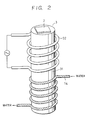
- Fig. 2 is a schematic perspective view of a substrate supporting device with a temperature controller, used in another embodiment of the present invention
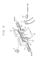
- Fig. 3 is a schematic illustration of an electric power supply holder with a temperature controller, used in still another embodiment of the present invention.
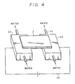
- Fig. 4 is a schematic perspective view of another example of the power supply holder of the present invention.
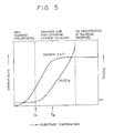
- Fig. 5 is a diagram showing the relationship between the substrate temperature and the growth rate and the quality of the diamond thin film.
- Fig. 1 is a schematic illustration of an embodiment of the apparatus of the present invention, applied to a system for forming a thin film by chemical vapor deposition employing a hot filament.
- Fig.5 a relationship as shown in Fig.5 exists between the substrate temperature and the rate of growth of diamond, as well as the quality of the crystal.
- the quality of the crystal is expressed in terms of a ratio Ind/Id between the peak intensity Ind of non-diamond carbon as impurity and the peak intensity Id of diamond, the peak intensities being determined through Raman spectral analysis of the deposited diamond.
- a smaller value of the ratio Ind/In indicates better quality of the diamond crystal.
- the growth rate and the purity of the diamond can be freely controlled by suitably setting the substrate temperature.
- a diamond of a high purity can be deposited at a low substrate temperature T A
- deposition at a substrate temperature T B enables diamond to deposit at a high growth rate although the purity is slightly reduced.
- the substrate temperature is controlled over a wide range and with good accuracy, in order to obtain a desired quality and growth rate of crystal.
- the apparatus has a reaction vessel 1 provided with a pressure gauge 17.
- the reaction vessel 1 accommodates a substrate supporting device 3 for supporting a substrate 2 on which a thin film is to be formed by deposition.
- the reaction vessel 1 also is provided with a work Port 11 through which the substrate 2 is brought into and out of the reaction vessel 1.
- the substrate supporting device 3 includes heating means 4 for heating the substrate 2 and a cooling means 5 under the heating means 4.
- the heating means 4 includes a thermocouple 13 and is capable of heating the substrate 2 when supplied with electric power through power terminals 12, while the cooling means 5 includes a cooling pipe 14 for circulating cooling water, a flowmeter 15 and a thermometer 16 for cooling water.
- the reaction vessel 1 also is provided at its upper or lower portions with a source gas supply port 7 and a gas exhaust port 8.
- a source gas such as CH4 gas diluted with H2 gas is introduced into the reaction vessel 1 through the source gas supply port 7 and is subjected to decompose and the resultant gas is exhausted through the exhaust port 8 by means of a vacuum pump 19.
- a hot filament 6 is disposed in the reaction vessel 1 which filament is connected to a power supply 18.
- a plasma may be used in place of the filament, as the decomposing means for decomposing the source gas.
- thermometer 9 e.g., a radiation pyrometer
- the apparatus has temperature control means 10 which includes, for example, a thermocouple voltage converter 21, a PID controller 22 and a thyristor regulator 23 for controlling the electric power supplied to the substrate heating means 4.
- the temperature controller 10 controls the operation of the heating means 4 in accordance with the substrate temperature measured by the non-contact type thermometer 9 or the thermocouple 13, thereby controlling the substrate temperature in combination with the cooling means 5.
- a switch 24 is provided for enabling change-over between the thermocouple 13 and the non-contact thermometer 9.
- the described arrangement in the apparatus of the present invention enables a control of the substrate temperature over a much wider temperature range than in known apparatuses in which the substrate temperature is controlled solely by heating or cooling.
- both the electric power and the cooling water are simultaneously supplied and the level of the electrical current is varied in accordance with a change in the substrate temperature, thereby maintaining the substrate temperature at a constant level.
- the substrate temperature can be controlled with much higher response speed and much better accuracy than in the case where the substrate temperature is controlled through a control of flow rate of the cooling water.
- there is no risk of boiling of the cooling water because a certain sufficient flow rate of the cooling water is maintained.
- FIG. 2 is a schematic perspective view of this embodiment.
- the substrate supporting device 3 for supporting a substrate 2 is a metal bar 31 on an upper portion of which is provided an RF heating coil 32 as the heating means 4, while a cooling water pipe 14 as the cooling means 5 is provided on a lower portion of the metal bar 31 by silver brazing.
- the present inventors also have considered an arrangement in which a substrate is held by a power supply holder which also serves as electrodes, the holder holding the substrate being placed in a reaction vessel of a reduced pressure so that an electric current is supplied through the power supply holder so as to heat the substrate.
- the inventors prepared test pieces of silicon substrates 50 mm long and 10 mm wide.
- the inventors connected electrodes to both ends of the test piece and supplied electric current to the test piece through these electrodes.
- the test piece was not red-heated at all when the voltage applied is still low.
- the substrate test piece was suddenly red-heated while drastically reducing its resistance from several k ⁇ to several ⁇ or below. It was confirmed through a measurement by a radiation pyrometer that the substrate surface temperature can be raised up to 1300°C by this method.
- the substrate test piece was uniformly red-heated over the entire portion thereof and enabled accurate measurement of the surface temperature. It was also confirmed that the temperature control can be done in a stable manner because the power supply holder, which will be detailed later, can stably hold the substrate without substantial change in the resistances at the contacts between the holder and the substrate.
- the apparatus employs a hot filament 6 for thermally decomposing the source gas.
- the apparatus also has a heating electric power supply 43 for supplying electric power which heats the substrate 2.
- a power supply holder 41 includes a power supply electrode 42 and an insulating means 44 for insulating the cooling means 5 from the substrate 2 and the power supply electrodes.
- the power supply holder 41 is capable of holding the substrate 2 and supplying the substrate 2 with an electric current from the heating electric power supply 43.
- the apparatus also has cooling means 5 which is held in contact with the power supply electrodes 42 through the insulating means 44.
- Numeral 47 designates a nozzle made of quartz which corresponds to the source gas supply port 7 and is capable of introducing the source gas into the zone near the surface of the substrate 2.
- Numeral 9 denotes a radiation pyrometer capable of measuring the substrate temperature in a non-contact manner. These components, except the radiation pyrometer, are encased in a reaction vessel as in the case of the embodiment shown in Fig. 1.
- the substrate 2 is disposed in the reaction vessel 1 such that its major surfaces are held vertically. This, however, is not exclusive and the power supply holder 41 and other components may be arranged horizontally so that the major surfaces of the substrate 2 extend substantially horizontally as in Fig. 1.
- the aforementioned radiation pyrometer 9 is disposed to oppose the reverse side, i.e.,the side opposite to the thin film depositing surface, of the substrate 2.
- the substrate 2 due to its high heat conductivity, exhibits almost the same temperature at both of its surfaces. It is therefore possible to accurately measure the temperature of the thin film depositing surface of the substrate by the radiation pyrometer 9 which senses the temperature of the surface of the substrate opposite to the depositing surface. If the substrate temperature is measured directly by contacting a thermocouple to the thin film depositing surface, a measuring error may be caused by influence of the heat radiated from the filament 6. Such an error, however, can be eliminated and a high accuracy of the temperature measurement is attained since the temperature is sensed and measured by the radiation pyrometer 9 which faces the reverse side of the substrate 2.
- the insulating means 44 are interposed between the cooling means 5 such as copper chill blocks and the power supply electrodes 42. More specifically, the arrangement is such that substrate 2 is received in slits 46 formed in the power supply electrodes 42 and pressing screws 45 are tightened to fix the substrate 2 between the power supply electrodes 42 and the insulating means 44.
- the insulating means 44 may be formed of an insulating material such as aluminum nitride plate. Although a quartz plate 2 can be used as the material of the insulating means 44, the use of aluminum nitride is preferred because this material exhibits a greater insulation and higher thermal conductivity than quartz. If the cooling means 5 is made of an insulating material or if the surface of the cooling means 5 is insulated, it is not necessary to interpose insulating means between the cooling means 5 and the electrodes 42.
- each power supply electrode 42 has a large cross-sectional area so as to reduce electrical resistance therethrough and is constructed to tightly contact with a large surface area of the substrate 2 so as to reduce the electrical and heat resistance across the contact between the power supply electrode 42 and the substrate 2.
- Fig.4 is a perspective view of another example of the power supply holder.
- the power supply holder employs a cooling means 5 through which cooling water is circulated.
- the substrate 2 is placed on the cooling means 5 such that the whole area of one surface of the substrate 2 contacts the cooling means 5.
- a pair of electrodes 42 are positioned in contact with two spaced portions of the upper surface of the substrate 2 so that the substrate 2 can be supplied with electric power through these electrodes 42 from a heating electric power supply 43.
- the substrate 2 itself functions as the heating means by electrically heating with electric power supplied thereto.
- the cooling means 5 is made of an electrically conductive material such as copper, it is necessary that an insulating means 44 is placed between the substrate 2 and the cooling means 5 as illustrated.
- Example 1 Example 1
- Diamond was deposited by hot filament CVD method, using the apparatus of the invention shown in Fig. 1.
- a silicon plate of 10 mm wide, 20 mm long and 0.5 mm thick was ground by diamond grains of particle size of about 20 ⁇ m, and used as the substrate 2.
- a tungsten filament 6 was set at a position about 2 mm apart from the deposition surface.
- the temperature of the filament during deposition was measured by an optical pyrometer,while the substrate temperature was measured by a sheet-type thermocouple of 0.07 mm thick.
- the power supply to the substrate 2 was adjusted so as to maintain the substrate temperature at any desired temperature between 500 and 1200°C.
- the temperature control could be done with a very small error of less than ⁇ 0.5°C.
- the deposition was conducted under the conditions of: a methane flow rate of 5 sccm, hydrogen flow rate of 500 sccm, atmospheric pressure of 30 Torr, filament temperature of 2100°C and substrate temperature of 850°C.
- Deposition of diamond film was confirmed by an observation through a scanning electron microscope and by Raman spectral analysis. A section of the film was observed by the scanning electron microscope for the measurement of the film thickness. The film growth rate was calculated from the film thickness to be 10 ⁇ m/hr. A micro-Raman spectral analysis was conducted on a plurality of points on a section of the film of 20 ⁇ m thick, for the measurement of the peak intensity Id exhibited by diamond and peak intensity Ind exhibited by non-diamond carbon. All these measuring points exhibited the same value of the ratio Ind/Id. The cooling was conducted by circulating cooling water of 25°C at a flow rate of 3 l/min. Example 2
- the CVD proces was carried out by using, as the source gas, CH4 gas diluted with hydrogen gas to 1% concentration.
- the source gas was supplied from the nozzle at a rate of 200 sccm onto the substrate 2 placed in the reaction vessel 1 in which an atmosphere of 30 Torr or lower pressure was maintained.
- the command substrate temperature was 870°C.
- a silicon plate of 10 mm wide, 20 mm long and 0.5 mm thick was used as the substrate.
- the temperature of the substrate surface could be controlled with a very small error of ⁇ 0.2°C with respect to the command temperature of 870°C, by virtue of the heating of the substrate with electrical current supplied to the substrate itself.
- the diamond film formed by this process exhibited a resistivity of 1013 to 1014 ⁇ m and a hardness Hv of 8000 to 9000 which well approximate those of natural diamonds, over the entire area of the film.
- the apparatus of the present invention makes it possible to form a thin film of uniform thickness and quality.
- the apparatus of the present invention can equally be applied to other CVD processes such as plasma-assisted CVD and to PVD (physical vapor deposition) processes such as sputtering PVD, and thin films of superior quality can be obtained also in such applications.
Landscapes
- Chemical & Material Sciences (AREA)
- General Chemical & Material Sciences (AREA)
- Chemical Kinetics & Catalysis (AREA)
- Engineering & Computer Science (AREA)
- Materials Engineering (AREA)
- Mechanical Engineering (AREA)
- Metallurgy (AREA)
- Organic Chemistry (AREA)
- Chemical Vapour Deposition (AREA)
- Crystals, And After-Treatments Of Crystals (AREA)
Applications Claiming Priority (4)
| Application Number | Priority Date | Filing Date | Title |
|---|---|---|---|
| JP312509/89 | 1989-12-01 | ||
| JP31250989 | 1989-12-01 | ||
| JP3949590A JPH02289494A (ja) | 1989-02-22 | 1990-02-20 | ダイヤモンドの合成装置 |
| JP39495/90 | 1990-02-20 |
Publications (2)
| Publication Number | Publication Date |
|---|---|
| EP0436070A1 true EP0436070A1 (fr) | 1991-07-10 |
| EP0436070B1 EP0436070B1 (fr) | 1995-02-01 |
Family
ID=26378907
Family Applications (1)
| Application Number | Title | Priority Date | Filing Date |
|---|---|---|---|
| EP90116005A Expired - Lifetime EP0436070B1 (fr) | 1989-12-01 | 1990-08-21 | Appareillage et procédé de depôt chimique en phase vapeur pour la production d'une couche mince |
Country Status (4)
| Country | Link |
|---|---|
| US (1) | US5225245A (fr) |
| EP (1) | EP0436070B1 (fr) |
| CA (1) | CA2023684A1 (fr) |
| DE (1) | DE69016633T2 (fr) |
Cited By (2)
| Publication number | Priority date | Publication date | Assignee | Title |
|---|---|---|---|---|
| EP0776988A3 (fr) * | 1995-12-01 | 1997-06-25 | Teisan Kk | |
| DE10239486A1 (de) * | 2002-08-21 | 2004-03-04 | Carl Zeiss Smt Ag | Verfahren zur Herstellung von teilbeschichteten Substraten |
Families Citing this family (9)
| Publication number | Priority date | Publication date | Assignee | Title |
|---|---|---|---|---|
| US6121061A (en) | 1997-11-03 | 2000-09-19 | Asm America, Inc. | Method of processing wafers with low mass support |
| JP4294140B2 (ja) * | 1999-01-27 | 2009-07-08 | 有限会社アプライドダイヤモンド | ダイヤモンド薄膜の改質方法及びダイヤモンド薄膜の改質及び薄膜形成方法並びにダイヤモンド薄膜の加工方法 |
| US6191399B1 (en) | 2000-02-01 | 2001-02-20 | Asm America, Inc. | System of controlling the temperature of a processing chamber |
| US6596973B1 (en) | 2002-03-07 | 2003-07-22 | Asm America, Inc. | Pyrometer calibrated wafer temperature estimator |
| US6818864B2 (en) * | 2002-08-09 | 2004-11-16 | Asm America, Inc. | LED heat lamp arrays for CVD heating |
| US6976782B1 (en) * | 2003-11-24 | 2005-12-20 | Lam Research Corporation | Methods and apparatus for in situ substrate temperature monitoring |
| US7833581B2 (en) * | 2006-09-11 | 2010-11-16 | The Hong Kong University Of Science And Technology | Method for making a highly stable diamond film on a substrate |
| US9885123B2 (en) | 2011-03-16 | 2018-02-06 | Asm America, Inc. | Rapid bake of semiconductor substrate with upper linear heating elements perpendicular to horizontal gas flow |
| US12195842B2 (en) * | 2019-11-11 | 2025-01-14 | Beijing Naura Microelectronics Equipment Co., Ltd. | Sputtering device with microwave heating mechanism |
Citations (2)
| Publication number | Priority date | Publication date | Assignee | Title |
|---|---|---|---|---|
| DE2808462A1 (de) * | 1977-03-02 | 1978-09-07 | Komatsu Mfg Co Ltd | Verfahren und vorrichtung zur herstellung von hochreinen siliziumstaeben |
| EP0276061A1 (fr) * | 1987-01-15 | 1988-07-27 | Varian Associates, Inc. | Dispositif pour déposition thermique rapide à partir d'une phase gazeuse |
-
1990
- 1990-08-17 US US07/568,857 patent/US5225245A/en not_active Expired - Fee Related
- 1990-08-21 CA CA002023684A patent/CA2023684A1/fr not_active Abandoned
- 1990-08-21 EP EP90116005A patent/EP0436070B1/fr not_active Expired - Lifetime
- 1990-08-21 DE DE69016633T patent/DE69016633T2/de not_active Expired - Fee Related
Patent Citations (2)
| Publication number | Priority date | Publication date | Assignee | Title |
|---|---|---|---|---|
| DE2808462A1 (de) * | 1977-03-02 | 1978-09-07 | Komatsu Mfg Co Ltd | Verfahren und vorrichtung zur herstellung von hochreinen siliziumstaeben |
| EP0276061A1 (fr) * | 1987-01-15 | 1988-07-27 | Varian Associates, Inc. | Dispositif pour déposition thermique rapide à partir d'une phase gazeuse |
Non-Patent Citations (3)
| Title |
|---|
| APPLIED SURFACE SCIENCE, vol. 33/34, 1988, pages 546-552; H. KANEKO et al.: "Influence of substrate- and atmospheric-temperatures on diamond deposition" * |
| PATENT ABSTRACTS OF JAPAN, vol. 10, no. 120 (C-343)[2177], 6th May 1986; & JP-A-60 245 776 (HITACHI SEISAKUSHO) 05-12-1985 * |
| PATENT ABSTRACTS OF JAPAN, vol. 10, no. 120 (C-343)[2177], 6th May 1986; & JP-A-60 245 778 (HITACHI SEISAKUSHO) 05-12-1985 * |
Cited By (3)
| Publication number | Priority date | Publication date | Assignee | Title |
|---|---|---|---|---|
| EP0776988A3 (fr) * | 1995-12-01 | 1997-06-25 | Teisan Kk | |
| US5892207A (en) * | 1995-12-01 | 1999-04-06 | Teisan Kabushiki Kaisha | Heating and cooling apparatus for reaction chamber |
| DE10239486A1 (de) * | 2002-08-21 | 2004-03-04 | Carl Zeiss Smt Ag | Verfahren zur Herstellung von teilbeschichteten Substraten |
Also Published As
| Publication number | Publication date |
|---|---|
| EP0436070B1 (fr) | 1995-02-01 |
| DE69016633D1 (de) | 1995-03-16 |
| DE69016633T2 (de) | 1995-05-24 |
| CA2023684A1 (fr) | 1991-06-02 |
| US5225245A (en) | 1993-07-06 |
Similar Documents
| Publication | Publication Date | Title |
|---|---|---|
| US5209182A (en) | Chemical vapor deposition apparatus for forming thin film | |
| Sommer et al. | Activity of tungsten and rhenium filaments in CH4/H2 and C2H2/H2 mixtures: Importance for diamond CVD | |
| US4935303A (en) | Novel diamond-like carbon film and process for the production thereof | |
| JP6353986B2 (ja) | 自立型cvd多結晶ダイアモンド膜を製造する装置および方法 | |
| EP0493609B1 (fr) | Procede et appareil pour travailler le diamant | |
| KR910001367B1 (ko) | 기상 합성 다이아몬드막 및 그 합성방법 | |
| US5525815A (en) | Diamond film structure with high thermal conductivity | |
| US5225245A (en) | Chemical vapor deposition method for forming thin film | |
| Liaw et al. | Epitaxial Growth and Characterization of β‐SiC Thin Films | |
| EP0526468B1 (fr) | Diamant sur substrat pour applications electroniques | |
| US5900225A (en) | Formation of diamond materials by rapid-heating and rapid-quenching of carbon-containing materials | |
| EP0964433A2 (fr) | Elément de chauffage céramique multicouche | |
| Jansen et al. | The deposition of diamond films by filament techniques | |
| WO1996005337A9 (fr) | Formation de matieres de type diamant par chauffage rapide et refroidissement rapide de materiaux contenant du carbone | |
| US6270898B1 (en) | Tool tip and bonding tool comprising the tool tip and control method for the bonding tool | |
| US6274837B1 (en) | Method and apparatus for in-situ solid state doping of CVD diamonds and diamonds so made | |
| Okano et al. | Synthesis of B-doped diamond film | |
| JPH01230496A (ja) | 新規なダイヤモンド状炭素膜及びその製造方法 | |
| US20230392255A1 (en) | Multiple Chamber System for Plasma Chemical Vapor Deposition of Diamond and Related Materials | |
| JPH03223197A (ja) | ダイヤモンドの気相合成装置及びその基板温度調整方法 | |
| Cherry et al. | Experimental apparatus for determining charge exchange between hydrogen and hydrocarbon groups in the hot filament deposition of diamond | |
| JP3637505B2 (ja) | N型半導体薄膜の製造方法及び薄膜サーミスタの製造方法 | |
| Böhm et al. | Influence of plasma parameters on the properties of diamond films deposited by the dc arc technique | |
| CN113026001A (zh) | 一种介稳态控制制备金刚石的方法 | |
| Li et al. | Diamond deposition using a grid filament |
Legal Events
| Date | Code | Title | Description |
|---|---|---|---|
| PUAI | Public reference made under article 153(3) epc to a published international application that has entered the european phase |
Free format text: ORIGINAL CODE: 0009012 |
|
| 17P | Request for examination filed |
Effective date: 19900821 |
|
| AK | Designated contracting states |
Kind code of ref document: A1 Designated state(s): DE FR GB |
|
| 17Q | First examination report despatched |
Effective date: 19921223 |
|
| GRAA | (expected) grant |
Free format text: ORIGINAL CODE: 0009210 |
|
| AK | Designated contracting states |
Kind code of ref document: B1 Designated state(s): DE FR GB |
|
| ET | Fr: translation filed | ||
| REF | Corresponds to: |
Ref document number: 69016633 Country of ref document: DE Date of ref document: 19950316 |
|
| PLBE | No opposition filed within time limit |
Free format text: ORIGINAL CODE: 0009261 |
|
| STAA | Information on the status of an ep patent application or granted ep patent |
Free format text: STATUS: NO OPPOSITION FILED WITHIN TIME LIMIT |
|
| 26N | No opposition filed | ||
| PGFP | Annual fee paid to national office [announced via postgrant information from national office to epo] |
Ref country code: FR Payment date: 20010810 Year of fee payment: 12 |
|
| PGFP | Annual fee paid to national office [announced via postgrant information from national office to epo] |
Ref country code: DE Payment date: 20010813 Year of fee payment: 12 |
|
| PGFP | Annual fee paid to national office [announced via postgrant information from national office to epo] |
Ref country code: GB Payment date: 20010815 Year of fee payment: 12 |
|
| REG | Reference to a national code |
Ref country code: GB Ref legal event code: IF02 |
|
| REG | Reference to a national code |
Ref country code: GB Ref legal event code: 732E |
|
| PG25 | Lapsed in a contracting state [announced via postgrant information from national office to epo] |
Ref country code: GB Free format text: LAPSE BECAUSE OF NON-PAYMENT OF DUE FEES Effective date: 20020821 |
|
| PG25 | Lapsed in a contracting state [announced via postgrant information from national office to epo] |
Ref country code: DE Free format text: LAPSE BECAUSE OF NON-PAYMENT OF DUE FEES Effective date: 20030301 |
|
| GBPC | Gb: european patent ceased through non-payment of renewal fee |
Effective date: 20020821 |
|
| PG25 | Lapsed in a contracting state [announced via postgrant information from national office to epo] |
Ref country code: FR Free format text: LAPSE BECAUSE OF NON-PAYMENT OF DUE FEES Effective date: 20030430 |
|
| REG | Reference to a national code |
Ref country code: FR Ref legal event code: ST |