EP0435406B1 - Verfahren zur Herstellung von Leistungsmos- und Halbleiteranordnungen und damit hergestellten Anordnungen - Google Patents
Verfahren zur Herstellung von Leistungsmos- und Halbleiteranordnungen und damit hergestellten Anordnungen Download PDFInfo
- Publication number
- EP0435406B1 EP0435406B1 EP90203503A EP90203503A EP0435406B1 EP 0435406 B1 EP0435406 B1 EP 0435406B1 EP 90203503 A EP90203503 A EP 90203503A EP 90203503 A EP90203503 A EP 90203503A EP 0435406 B1 EP0435406 B1 EP 0435406B1
- Authority
- EP
- European Patent Office
- Prior art keywords
- layer
- gate
- formation
- slice
- spacer
- Prior art date
- Legal status (The legal status is an assumption and is not a legal conclusion. Google has not performed a legal analysis and makes no representation as to the accuracy of the status listed.)
- Expired - Lifetime
Links
Images

Classifications
-
- H—ELECTRICITY
- H10—SEMICONDUCTOR DEVICES; ELECTRIC SOLID-STATE DEVICES NOT OTHERWISE PROVIDED FOR
- H10D—INORGANIC ELECTRIC SEMICONDUCTOR DEVICES
- H10D30/00—Field-effect transistors [FET]
- H10D30/60—Insulated-gate field-effect transistors [IGFET]
- H10D30/64—Double-diffused metal-oxide semiconductor [DMOS] FETs
- H10D30/66—Vertical DMOS [VDMOS] FETs
-
- H—ELECTRICITY
- H10—SEMICONDUCTOR DEVICES; ELECTRIC SOLID-STATE DEVICES NOT OTHERWISE PROVIDED FOR
- H10P—GENERIC PROCESSES OR APPARATUS FOR THE MANUFACTURE OR TREATMENT OF DEVICES COVERED BY CLASS H10
- H10P95/00—Generic processes or apparatus for manufacture or treatments not covered by the other groups of this subclass
-
- H—ELECTRICITY
- H10—SEMICONDUCTOR DEVICES; ELECTRIC SOLID-STATE DEVICES NOT OTHERWISE PROVIDED FOR
- H10D—INORGANIC ELECTRIC SEMICONDUCTOR DEVICES
- H10D30/00—Field-effect transistors [FET]
- H10D30/01—Manufacture or treatment
- H10D30/021—Manufacture or treatment of FETs having insulated gates [IGFET]
- H10D30/028—Manufacture or treatment of FETs having insulated gates [IGFET] of double-diffused metal oxide semiconductor [DMOS] FETs
- H10D30/0291—Manufacture or treatment of FETs having insulated gates [IGFET] of double-diffused metal oxide semiconductor [DMOS] FETs of vertical DMOS [VDMOS] FETs
-
- H—ELECTRICITY
- H10—SEMICONDUCTOR DEVICES; ELECTRIC SOLID-STATE DEVICES NOT OTHERWISE PROVIDED FOR
- H10D—INORGANIC ELECTRIC SEMICONDUCTOR DEVICES
- H10D62/00—Semiconductor bodies, or regions thereof, of devices having potential barriers
- H10D62/80—Semiconductor bodies, or regions thereof, of devices having potential barriers characterised by the materials
- H10D62/83—Semiconductor bodies, or regions thereof, of devices having potential barriers characterised by the materials being Group IV materials, e.g. B-doped Si or undoped Ge
-
- H—ELECTRICITY
- H10—SEMICONDUCTOR DEVICES; ELECTRIC SOLID-STATE DEVICES NOT OTHERWISE PROVIDED FOR
- H10D—INORGANIC ELECTRIC SEMICONDUCTOR DEVICES
- H10D64/00—Electrodes of devices having potential barriers
- H10D64/60—Electrodes characterised by their materials
- H10D64/62—Electrodes ohmically coupled to a semiconductor
-
- H—ELECTRICITY
- H10—SEMICONDUCTOR DEVICES; ELECTRIC SOLID-STATE DEVICES NOT OTHERWISE PROVIDED FOR
- H10D—INORGANIC ELECTRIC SEMICONDUCTOR DEVICES
- H10D64/00—Electrodes of devices having potential barriers
- H10D64/60—Electrodes characterised by their materials
- H10D64/66—Electrodes having a conductor capacitively coupled to a semiconductor by an insulator, e.g. MIS electrodes
- H10D64/661—Electrodes having a conductor capacitively coupled to a semiconductor by an insulator, e.g. MIS electrodes the conductor comprising a layer of silicon contacting the insulator, e.g. polysilicon having vertical doping variation
- H10D64/662—Electrodes having a conductor capacitively coupled to a semiconductor by an insulator, e.g. MIS electrodes the conductor comprising a layer of silicon contacting the insulator, e.g. polysilicon having vertical doping variation the conductor further comprising additional layers, e.g. multiple silicon layers having different crystal structures
- H10D64/663—Electrodes having a conductor capacitively coupled to a semiconductor by an insulator, e.g. MIS electrodes the conductor comprising a layer of silicon contacting the insulator, e.g. polysilicon having vertical doping variation the conductor further comprising additional layers, e.g. multiple silicon layers having different crystal structures the additional layers comprising a silicide layer contacting the layer of silicon, e.g. polycide gates
-
- Y—GENERAL TAGGING OF NEW TECHNOLOGICAL DEVELOPMENTS; GENERAL TAGGING OF CROSS-SECTIONAL TECHNOLOGIES SPANNING OVER SEVERAL SECTIONS OF THE IPC; TECHNICAL SUBJECTS COVERED BY FORMER USPC CROSS-REFERENCE ART COLLECTIONS [XRACs] AND DIGESTS
- Y10—TECHNICAL SUBJECTS COVERED BY FORMER USPC
- Y10S—TECHNICAL SUBJECTS COVERED BY FORMER USPC CROSS-REFERENCE ART COLLECTIONS [XRACs] AND DIGESTS
- Y10S148/00—Metal treatment
- Y10S148/126—Power FETs
Definitions
- the present invention relates to a process of manufacture of power-MOS semiconductor devices with high density of the elementary MOS cells as well as the power-MOS devices obtained by said process.
- the minimum dimensions of the cell obtained in accordance with conventional processes are conditioned by the resolving power and the alignment limits of the photographic exposure system used, as well as the tolerances imposed by the various steps of the production process. More precisely, the minimal dimensions Xc are determined by the requirement to effect three successive alignments inside the polycrystalline silicon. and by the technological limit associated with the smallest possible openings. Using conventional photographic exposure equipment with projection the minimal dimensions of Xc are approximately 8 ⁇ m.
- the smallest side dimensions of the gate (Xd) are linked to the requirement of allowing sufficiently deep diffusion of the body dopant to prevent the formation of short circuits due to the so-called spikes of aluminium which occur in conventional metallizations. Said minimal dimensions of Xd are approximately 6-7 ⁇ m regardless of the technique used.
- the object of the present invention is to considerably reduce the minimal dimensions of the elementary cells (Xpitch) of a power-MOS device so as to increase the density of integration of the corresponding devices and at the same time simplify the manufacturing process.
- the process for manufacture of power-MOS semiconductor devices in accordance with the invention comprises the steps described in following claim 1.
- the process comprises in sequence the following steps. of which the initial ones, specifically from a. to d., are already provided for in the known art.
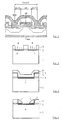
- FIG. 11 The structure of the device obtained at the end of the process is shown schematically in FIG. 11.
- Step o. of the process indicated above may be carried out later. Indeed, implantation of dopant for formation of the source regions can take place without previous stripping of the layer of Si3N4.
- photolithographic exposure equipment of the 5:1 stepper type which allows minimum apertures on the order of 1 ⁇ m with maximum misalignment between two successive photoengravings of .35 ⁇ m.
- Xc can be approximately 1.8 ⁇ m.
- Xd about 1 ⁇ m.
- the Xc dimension is conditioned by a single alignment and can fall to values of approximately 1.8 ⁇ m while Xd can fall to values of approximately 1 ⁇ m.
- Silicides on the source, on the body and on the gate polysilicon allow considerable reduction of the increase in parasite resistances due to the considerable reduction of the metal/semiconductor contact areas on the active regions and reduction of the increase in the resistance of the gate poly due to high integration. This also allows elimination of the risk of spikes on the aluminium of the metallization and consequently permits reduction of the body depth (not more than .4 ⁇ m) and the side dimensions of the body and gate.
- the RTA process makes it possible to limit the side growth or the silicide on the spacer, which would otherwise risk short circuiting the gate with the other electrodes.
- one of the variants can provide in step t. of the above described process the deposition of another refractory metal such as Co, W or an alloy thereof and in the latter case the formation of the related silicides in step u.
- another refractory metal such as Co, W or an alloy thereof
- Another variant can consist of effecting a further self-aligned ionic implantation of dopant to form a deep body P+ region between steps i. and l. described above.
Landscapes
- Electrodes Of Semiconductors (AREA)
- Insulated Gate Type Field-Effect Transistor (AREA)
Claims (6)
- Verfahren zur Herstellung von Leistungs-MOS-Halbleiter-Anordnungen, das die folgenden Schritte umfaßt:- auf einem Siliziumsubstrat mit einem ersten Leitungstyp erfolgendes epitaktisches Wachstum mindestens einer Schicht aus Silizium des selben Leitungstyps,- Gate-Oxidation auf dem gesamten Wafer,- Abscheidung einer Schicht aus polykristallinem Silizium auf der Stirnseite des Wafers,- Ausnehmung eines Fensters - im folgenden "Gate-Fenster" genannt - in der Schicht aus polykristallinem Silizium mittels Photolithographie zur Festlegung des Gate-Polysiliziums,- Implantation und Eindiffundieren einer Dotierung eines zweiten Leitungstyps an dem vorhergenannten Gate-Fenster zur Bildung der Masse,- Implantation und Eindiffundieren einer Dotierung eines ersten Leitungstyps in die Masse zur Bildung der Source-Bereiche,- Abscheidung eines p-Vapox-Dielektrikums auf der Stirnseite des Wafers,- Ausnehmung von Fenstern auf der Stirnseite des Wafers zur Bildung der Sourcekontakte, und- Abscheidung von Aluminium auf der Stirnseite des Wafers, um einen Metallbelag der Source- und Gate-Schichten bereitzustellen, dadurch gekennzeichnet, daß
die Ausnehmung des obigen Gate-Fensters in der polykristallinen Siliziumschicht gefolgt wird durch:- Ionenimplantation einer Dotierung eines zweiten Leitungstyps in die Oberfläche des Wafers an dem Fenster zur Bildung der Masse (8),- CVD-Abscheidung einer dünnen Schicht (5) aus Siliziumnitrid Si₃N₄ über dem gesamten Wafer,- CVD-Abscheidung einer Schicht (6) eines Dielektrikums auf der Oberfläche des Wafers,- RIE der Schicht (6) eines Dielektrikums, um einen Abstandhalter (7) entlang der Wände des Gate-Fensters bereitzustellen,- Ätzen der Siliziumnitridschicht (5) in dem nicht durch den Abstandhalter geschützten Bereich,- Ablösen des Abstandhalters (7), um so das darunterliegende Siliziumnitrid aufzudecken,- Eindiffundieren der implantierten Dotierung zur Bildung des Massebereiches (8) und Bildung von Schichten (10, 9) aus Siliziumdioxid jeweils entsprechend auf dem Gate-Poly und der Masse unter Verwendung der Locos-Technologie,- Ablösen des Nitrids (5) von dem vorher durch den Abstandhalter (7) besetzten Bereich,- Verwendung der auf der Masse ausgebildeten Schicht (9) aus Siliziumdioxid als eine Maske zur Implantation oder Vorabscheidung einer Dotierung eines ersten Leitungstyps und nachfolgendes Eindiffundieren, um die Source-Bereiche (12) bereitzustellen,- Ablösen der vorher auf der Masse und dem Gate-Poly ausgebildeten Schichten (9, 10) aus Dioxid,- Erzeugung eines weiteren Abstandhalters (14) aus dielektrischem Material entlang der Gate-Wände,- Metallabscheidung der Source- und Gate-Kontaktflächen durch Abscheidung einer Schicht (15) aus hitzebeständigem Material und Brennen mittels RTA zur Bildung eines Silizids,- selektives Ätzen zur Beseitigung des hitzebeständigen Metalls, das den weiteren Abstandhalter bedeckt, gefolgt durch ein weiteres Brennen des Silizids mittles RTA,- Abscheidung eines Dielektrikums auf der Stirnseite des Wafers und Ausnehmung von Fenstern zur Bildung der Source-Kontake. - Verfahren zur Herstellung von Leistungs-MOS-Halbleiter-Anordnungen, das die folgenden Schritte umfaßt:- auf einem Siliziumsubstrat mit einem ersten Leitungstyp erfolgendes epitaktisches Wachstum mindestens einer Schicht aus Silizium des selben Leitungstyps,- Gate-Oxidation auf dem gesamten Wafer,- Abscheidung einer Schicht aus polykristallinem Silizium auf der Stirnseite des Wafers,- Ausnehmung eines Fensters - im folgenden "Gate-Fenster" genannt - in der Schicht aus polykristallinem Silizium mittels Photolithographie zur Festlegung des Gate-Polysiliziums,- Implantation und Eindiffundieren einer Dotierung eines zweiten Leitungstyps an dem vorhergenannten Gate-Fenster zur Bildung der Masse,- Implantation und Eindiffundieren einer Dotierung eines ersten Leitungstyps in der Masse zur Bildung der Source-Bereiche,- Abscheidung eines p-Vapox-Dielektrikums auf der Stirnseite des Wafers,- Ausnehmung von Fenstern auf der Stirnseite des Wafers zur Bildung der Sourcekontakte, und- Abscheidung von Aluminium auf der Stirnseite des Wafers, um einen Metallbelag der Source- und Gate-Schichten bereitzustellen, dadurch gekennzeichnet, daß
die Ausnehmung des obigen Gate-Fensters in der polykristallinen Siliziumschicht gefolgt wird durch:- Ionenimplantation einer Dotierung eines zweiten Leitungstyps in die Oberfläche des Wafers an dem Fenster zur Bildung der Masse (8),- CVD-Abscheidung einer dünnen Schicht (5) aus Siliziumnitrid Si₃N₄ über dem gesamten Wafer,- CVD-Abscheidung einer Schicht (6) eines Dielektrikums auf der Oberfläche des Wafers,- RIE der Schicht (6) eines Dielektrikums, um einen Abstandhalter (7) entlang der Wände des Gate-Fensters bereitzustellen,- Ätzen der Siliziumnitridschicht (5) in dem nicht durch den Abstandhalter geschützten Bereich,- Ablösen des Abstandhalters (7), um so das darunterliegende Siliziumnitrid aufzudecken,- Eindiffundieren der implantierten Dotierung zur Bildung des Massebereiches (8) und Bildung von Schichten (9, 10) aus Siliziumdioxid jeweils entsprechend auf dem Gate-Poly und der Masse unter Verwendung der Locos-Technologie,- Verwendung der auf der Masse ausgebildeten Siliziumdioxidschicht (9) als eine Maske zur Implantation einer Dotierung eines ersten Leitungstyps durch die Siliziumnitiridschicht und nachfolgendes Eindiffundieren zur Bereitstellung der Source-Bereiche (12),- Ablösen des Nitrids (5) von dem vorher durch den Abstandhalter (7) besetzten Bereich,- Ablösen der vorher auf der Masse und dem Gate-Poly ausgebildeten Schichten (9, 10) aus Dioxid,- Erzeugung eines weiteren Abstandhalters (14) aus dielektrischem Material entlang der Gate-Wände,- Metallabscheidung der Source- und Gate-Kontaktflächen durch Abscheidung einer Schicht (15) aus hitzebeständigem Material und Bildung eines Silizids durch Brennen mittels RTA,- selektives Ätzen zur Beseitigung des hitzebeständigen Metalls, das den weiteren Abstandhalter bedeckt, gefolgt durch ein weiteres Brennen des Silizids mittels RTA,- Abscheidung eines Dielektrikums auf der Stirnseite des Wafers und Ausnehmung von Fenstern zur Bildung der Source-Kontake. - Verfahren gemäß den Ansprüchen 1 oder 2, dadurch gekenn zeichnet, daß das Ätzen der Siliziumnitridschicht (5) in den nicht durch den Abstandhalter geschützten Bereichen von einer zweiten Ionenimplantation einer Dotierung eines zweiten Leitungstyps an dem durch den Abstandhalter (7) gebildeten Fenster zu Bildung eines tiefen Massebereiches und weiterhin durch ein Ablösen des Abstandhalters und durch das nachfolgende Eindiffundieren der implantierten Dotierung zur Bildung der Masse und der tiefen Massebereiche gefolgt wird.
- Verfahren gemäß den Ansprüchen 1 oder 2, dadurch gekenn zeichnet, daß:- die Siliziumnitridschicht (5) eine Dicke zwischen 20 und 40 nm (200 und 400 Ångström) besitzt,- die dielektrische Schicht (6) aus Siliziumdioxid SiO₂ besteht und eine Dicke von ungefähr 500 nm (5000 Ångström) besitzt,- die Erzeugung des Abstandhalters (14) durch die Abscheidung einer Schicht aus Siliziumdioxid SiO₂ vorgesehen ist, die eine Dicke von ungefähr 150 nm (1500 Ångström) besitzt.
- Verfahren gemäß Anspruch 1, dadurch gekennzeichnet, daß die photolithographischen Verfahren unter Verwendung einer photolithographischen Belichtungsapparatur des 5:1-Stufen-Typs stattfinden.
- Verfahren gemäß Anspruch 1, dadurch gekennzeichnet, daß zur Metallabscheidung der Masse-, Source- und Gate-Kontaktflächen Silizide von Titan oder Kobalt oder Wolfram oder deren Legierungen verwendet werden.
Applications Claiming Priority (2)
| Application Number | Priority Date | Filing Date | Title |
|---|---|---|---|
| IT02289189A IT1236994B (it) | 1989-12-29 | 1989-12-29 | Processo per la fabbricazione di dispositivi semiconduttori mos di potenza e dispositivi con esso ottenuti |
| IT2289189 | 1989-12-29 |
Publications (2)
| Publication Number | Publication Date |
|---|---|
| EP0435406A1 EP0435406A1 (de) | 1991-07-03 |
| EP0435406B1 true EP0435406B1 (de) | 1994-03-16 |
Family
ID=11201599
Family Applications (1)
| Application Number | Title | Priority Date | Filing Date |
|---|---|---|---|
| EP90203503A Expired - Lifetime EP0435406B1 (de) | 1989-12-29 | 1990-12-24 | Verfahren zur Herstellung von Leistungsmos- und Halbleiteranordnungen und damit hergestellten Anordnungen |
Country Status (6)
| Country | Link |
|---|---|
| US (1) | US5141883A (de) |
| EP (1) | EP0435406B1 (de) |
| JP (1) | JPH04305978A (de) |
| KR (1) | KR100202048B1 (de) |
| DE (1) | DE69007449T2 (de) |
| IT (1) | IT1236994B (de) |
Cited By (1)
| Publication number | Priority date | Publication date | Assignee | Title |
|---|---|---|---|---|
| DE19959346B4 (de) * | 1999-12-09 | 2004-08-26 | Micronas Gmbh | Verfahren zum Herstellen eines eine Mikrostruktur aufweisenden Festkörpers |
Families Citing this family (10)
| Publication number | Priority date | Publication date | Assignee | Title |
|---|---|---|---|---|
| US5288653A (en) * | 1991-02-27 | 1994-02-22 | Nec Corporation | Process of fabricating an insulated-gate field effect transistor |
| DE69434268T2 (de) * | 1994-07-14 | 2006-01-12 | Stmicroelectronics S.R.L., Agrate Brianza | Intergrierte Struktur einer Hochgeschwindigkeits-MOS-Technologe-Leistungsvorrichtung und zugehöriges Herstellungsverfahren |
| US5474946A (en) * | 1995-02-17 | 1995-12-12 | International Rectifier Corporation | Reduced mask process for manufacture of MOS gated devices |
| US5595918A (en) * | 1995-03-23 | 1997-01-21 | International Rectifier Corporation | Process for manufacture of P channel MOS-gated device |
| US5830798A (en) * | 1996-01-05 | 1998-11-03 | Micron Technology, Inc. | Method for forming a field effect transistor |
| KR100204805B1 (ko) * | 1996-12-28 | 1999-06-15 | 윤종용 | 디엠오에스 트랜지스터 제조방법 |
| EP0993033A1 (de) | 1998-10-06 | 2000-04-12 | STMicroelectronics S.r.l. | Gate-Isolierungsstruktur für Leistungs-MOS-Transistor und Herstellungsverfahren dafür |
| US6214673B1 (en) * | 1999-07-09 | 2001-04-10 | Intersil Corporation | Process for forming vertical semiconductor device having increased source contact area |
| US7166232B2 (en) | 2000-12-21 | 2007-01-23 | Micronas Gmbh | Method for producing a solid body including a microstructure |
| ITVA20010045A1 (it) * | 2001-12-14 | 2003-06-16 | St Microelectronics Srl | Flusso di processo per la realizzazione di un vdmos a canale scalato e basso gradiente di body per prestazioni ad elevata densita' di corren |
Family Cites Families (14)
| Publication number | Priority date | Publication date | Assignee | Title |
|---|---|---|---|---|
| US4443931A (en) * | 1982-06-28 | 1984-04-24 | General Electric Company | Method of fabricating a semiconductor device with a base region having a deep portion |
| US4489481A (en) * | 1982-09-20 | 1984-12-25 | Texas Instruments Incorporated | Insulator and metallization method for VLSI devices with anisotropically-etched contact holes |
| US4677735A (en) * | 1984-05-24 | 1987-07-07 | Texas Instruments Incorporated | Method of providing buried contacts for N and P channel devices in an SOI-CMOS process using a single N+polycrystalline silicon layer |
| IT1213234B (it) * | 1984-10-25 | 1989-12-14 | Sgs Thomson Microelectronics | Procedimento perfezionato per la fabbricazione di dispositivi a semiconduttore dmos. |
| EP0229362B1 (de) * | 1986-01-10 | 1993-03-17 | General Electric Company | Halbleitervorrichtung und Methode zur Herstellung |
| IT1204243B (it) * | 1986-03-06 | 1989-03-01 | Sgs Microelettronica Spa | Procedimento autoallineato per la fabbricazione di celle dmos di piccole dimensioni e dispositivi mos ottenuti mediante detto procedimento |
| US4798810A (en) * | 1986-03-10 | 1989-01-17 | Siliconix Incorporated | Method for manufacturing a power MOS transistor |
| US4716126A (en) * | 1986-06-05 | 1987-12-29 | Siliconix Incorporated | Fabrication of double diffused metal oxide semiconductor transistor |
| US4842675A (en) * | 1986-07-07 | 1989-06-27 | Texas Instruments Incorporated | Integrated circuit isolation process |
| US4772569A (en) * | 1986-10-30 | 1988-09-20 | Mitsubishi Denki Kabushiki Kaisha | Method for forming oxide isolation films on french sidewalls |
| US4735680A (en) * | 1986-11-17 | 1988-04-05 | Yen Yung Chau | Method for the self-aligned silicide formation in IC fabrication |
| JP2604777B2 (ja) * | 1988-01-18 | 1997-04-30 | 松下電工株式会社 | 二重拡散型電界効果半導体装置の製法 |
| US4949136A (en) * | 1988-06-09 | 1990-08-14 | University Of Connecticut | Submicron lightly doped field effect transistors |
| US4985740A (en) * | 1989-06-01 | 1991-01-15 | General Electric Company | Power field effect devices having low gate sheet resistance and low ohmic contact resistance |
-
1989
- 1989-12-29 IT IT02289189A patent/IT1236994B/it active IP Right Grant
-
1990
- 1990-12-24 DE DE69007449T patent/DE69007449T2/de not_active Expired - Fee Related
- 1990-12-24 US US07/632,485 patent/US5141883A/en not_active Expired - Lifetime
- 1990-12-24 EP EP90203503A patent/EP0435406B1/de not_active Expired - Lifetime
- 1990-12-28 KR KR1019900022248A patent/KR100202048B1/ko not_active Expired - Fee Related
- 1990-12-28 JP JP2418101A patent/JPH04305978A/ja active Pending
Non-Patent Citations (2)
| Title |
|---|
| Book "Integrated Circuit Mask Technology", 1985, pp. 160-165, Ed. Mc Graw-Hill Book Co., by D.J.Elliott * |
| Electronic Letters, Vol.25, Nr.16, 3rd August 1988, pp.1033-1034 * |
Cited By (1)
| Publication number | Priority date | Publication date | Assignee | Title |
|---|---|---|---|---|
| DE19959346B4 (de) * | 1999-12-09 | 2004-08-26 | Micronas Gmbh | Verfahren zum Herstellen eines eine Mikrostruktur aufweisenden Festkörpers |
Also Published As
| Publication number | Publication date |
|---|---|
| IT1236994B (it) | 1993-05-12 |
| KR100202048B1 (ko) | 1999-06-15 |
| DE69007449T2 (de) | 1994-08-25 |
| EP0435406A1 (de) | 1991-07-03 |
| JPH04305978A (ja) | 1992-10-28 |
| KR910013450A (ko) | 1991-08-08 |
| US5141883A (en) | 1992-08-25 |
| DE69007449D1 (de) | 1994-04-21 |
| IT8922891A0 (it) | 1989-12-29 |
Similar Documents
| Publication | Publication Date | Title |
|---|---|---|
| US5231038A (en) | Method of producing field effect transistor | |
| KR100352715B1 (ko) | 서브미크론금속게이트mos트랜지스터및그의형성방법 | |
| JP2605008B2 (ja) | 半導体装置の製造方法 | |
| US4384301A (en) | High performance submicron metal-oxide-semiconductor field effect transistor device structure | |
| US6852597B2 (en) | Method for fabricating power semiconductor device having trench gate structure | |
| US4102733A (en) | Two and three mask process for IGFET fabrication | |
| US5849616A (en) | Method of manufacturing a semiconductor device | |
| EP0179407B1 (de) | Verfahren zum Herstellen einer DMOS-Halbleiteranordnung | |
| US6252277B1 (en) | Embedded polysilicon gate MOSFET | |
| US5879994A (en) | Self-aligned method of fabricating terrace gate DMOS transistor | |
| US6261915B1 (en) | Process of making polysilicon resistor | |
| US5783474A (en) | Reduced mask process for manufacture of MOS gated devices using dopant-enhanced-oxidation of semiconductor | |
| KR19980018751A (ko) | 반도체 장치 및 그 제조 방법 (semiconductor device and method of manufacturing the same) | |
| US4985746A (en) | Semiconductor device and method of production | |
| JP2668081B2 (ja) | Cmosepromメモリセルを製造する方法 | |
| US4939154A (en) | Method of fabricating an insulated gate semiconductor device having a self-aligned gate | |
| EP0404372B1 (de) | Verfahren zur Herstellung von polykristallinen Siliziumkontakten | |
| US5141883A (en) | Process for the manufacture of power-mos semiconductor devices | |
| US5234851A (en) | Small cell, low contact assistance rugged power field effect devices and method of fabrication | |
| US5225357A (en) | Low P+ contact resistance formation by double implant | |
| US4076557A (en) | Method for providing semiconductor devices | |
| US6078079A (en) | Semiconductor device and method of manufacturing the same | |
| US4621412A (en) | Manufacturing a complementary MOSFET | |
| JPH05251694A (ja) | Mos型半導体装置及びその製造方法 | |
| US6686276B2 (en) | Semiconductor chip having both polycide and salicide gates and methods for making same |
Legal Events
| Date | Code | Title | Description |
|---|---|---|---|
| PUAI | Public reference made under article 153(3) epc to a published international application that has entered the european phase |
Free format text: ORIGINAL CODE: 0009012 |
|
| AK | Designated contracting states |
Kind code of ref document: A1 Designated state(s): DE FR GB NL |
|
| 17P | Request for examination filed |
Effective date: 19911223 |
|
| 17Q | First examination report despatched |
Effective date: 19920512 |
|
| GRAA | (expected) grant |
Free format text: ORIGINAL CODE: 0009210 |
|
| AK | Designated contracting states |
Kind code of ref document: B1 Designated state(s): DE FR GB NL |
|
| PG25 | Lapsed in a contracting state [announced via postgrant information from national office to epo] |
Ref country code: NL Effective date: 19940316 |
|
| REF | Corresponds to: |
Ref document number: 69007449 Country of ref document: DE Date of ref document: 19940421 |
|
| ET | Fr: translation filed | ||
| NLV1 | Nl: lapsed or annulled due to failure to fulfill the requirements of art. 29p and 29m of the patents act | ||
| PLBE | No opposition filed within time limit |
Free format text: ORIGINAL CODE: 0009261 |
|
| STAA | Information on the status of an ep patent application or granted ep patent |
Free format text: STATUS: NO OPPOSITION FILED WITHIN TIME LIMIT |
|
| 26N | No opposition filed | ||
| REG | Reference to a national code |
Ref country code: FR Ref legal event code: D6 |
|
| REG | Reference to a national code |
Ref country code: GB Ref legal event code: IF02 |
|
| PGFP | Annual fee paid to national office [announced via postgrant information from national office to epo] |
Ref country code: FR Payment date: 20021210 Year of fee payment: 13 |
|
| PGFP | Annual fee paid to national office [announced via postgrant information from national office to epo] |
Ref country code: GB Payment date: 20021218 Year of fee payment: 13 |
|
| PGFP | Annual fee paid to national office [announced via postgrant information from national office to epo] |
Ref country code: DE Payment date: 20021231 Year of fee payment: 13 |
|
| PG25 | Lapsed in a contracting state [announced via postgrant information from national office to epo] |
Ref country code: GB Free format text: LAPSE BECAUSE OF NON-PAYMENT OF DUE FEES Effective date: 20031224 |
|
| PG25 | Lapsed in a contracting state [announced via postgrant information from national office to epo] |
Ref country code: DE Free format text: LAPSE BECAUSE OF NON-PAYMENT OF DUE FEES Effective date: 20040701 |
|
| GBPC | Gb: european patent ceased through non-payment of renewal fee |
Effective date: 20031224 |
|
| PG25 | Lapsed in a contracting state [announced via postgrant information from national office to epo] |
Ref country code: FR Free format text: LAPSE BECAUSE OF NON-PAYMENT OF DUE FEES Effective date: 20040831 |
|
| REG | Reference to a national code |
Ref country code: FR Ref legal event code: ST |