US4985746A - Semiconductor device and method of production - Google Patents
Semiconductor device and method of production Download PDFInfo
- Publication number
- US4985746A US4985746A US07/075,245 US7524587A US4985746A US 4985746 A US4985746 A US 4985746A US 7524587 A US7524587 A US 7524587A US 4985746 A US4985746 A US 4985746A
- Authority
- US
- United States
- Prior art keywords
- region
- drain
- semiconductor device
- source
- polycrystalline silicon
- Prior art date
- Legal status (The legal status is an assumption and is not a legal conclusion. Google has not performed a legal analysis and makes no representation as to the accuracy of the status listed.)
- Expired - Lifetime
Links
- 239000004065 semiconductor Substances 0.000 title claims abstract description 29
- 238000000034 method Methods 0.000 title abstract description 16
- 238000004519 manufacturing process Methods 0.000 title abstract description 9
- 229910021420 polycrystalline silicon Inorganic materials 0.000 claims abstract description 40
- 229910021332 silicide Inorganic materials 0.000 claims abstract description 15
- FVBUAEGBCNSCDD-UHFFFAOYSA-N silicide(4-) Chemical compound [Si-4] FVBUAEGBCNSCDD-UHFFFAOYSA-N 0.000 claims abstract description 15
- 238000009792 diffusion process Methods 0.000 claims description 18
- 239000000758 substrate Substances 0.000 claims description 9
- DFJQEGUNXWZVAH-UHFFFAOYSA-N bis($l^{2}-silanylidene)titanium Chemical compound [Si]=[Ti]=[Si] DFJQEGUNXWZVAH-UHFFFAOYSA-N 0.000 claims description 6
- 229910008814 WSi2 Inorganic materials 0.000 claims description 3
- 229910052751 metal Inorganic materials 0.000 claims description 3
- 239000002184 metal Substances 0.000 claims description 3
- YXTPWUNVHCYOSP-UHFFFAOYSA-N bis($l^{2}-silanylidene)molybdenum Chemical compound [Si]=[Mo]=[Si] YXTPWUNVHCYOSP-UHFFFAOYSA-N 0.000 claims description 2
- WQJQOUPTWCFRMM-UHFFFAOYSA-N tungsten disilicide Chemical compound [Si]#[W]#[Si] WQJQOUPTWCFRMM-UHFFFAOYSA-N 0.000 claims description 2
- 239000011810 insulating material Substances 0.000 claims 1
- 229920005591 polysilicon Polymers 0.000 abstract description 29
- 229910052698 phosphorus Inorganic materials 0.000 abstract description 26
- 230000010354 integration Effects 0.000 abstract description 5
- 230000015572 biosynthetic process Effects 0.000 abstract description 4
- 238000000151 deposition Methods 0.000 abstract description 2
- -1 boron ions Chemical class 0.000 description 15
- 229910052796 boron Inorganic materials 0.000 description 9
- 230000008569 process Effects 0.000 description 7
- XUIMIQQOPSSXEZ-UHFFFAOYSA-N Silicon Chemical compound [Si] XUIMIQQOPSSXEZ-UHFFFAOYSA-N 0.000 description 5
- 230000005540 biological transmission Effects 0.000 description 5
- 229910052710 silicon Inorganic materials 0.000 description 5
- 239000010703 silicon Substances 0.000 description 5
- 229910008479 TiSi2 Inorganic materials 0.000 description 4
- 230000000694 effects Effects 0.000 description 4
- 238000005530 etching Methods 0.000 description 4
- 238000002347 injection Methods 0.000 description 4
- 239000007924 injection Substances 0.000 description 4
- 239000011574 phosphorus Substances 0.000 description 4
- 238000001259 photo etching Methods 0.000 description 4
- QGZKDVFQNNGYKY-UHFFFAOYSA-N Ammonia Chemical compound N QGZKDVFQNNGYKY-UHFFFAOYSA-N 0.000 description 3
- 229910052782 aluminium Inorganic materials 0.000 description 3
- XAGFODPZIPBFFR-UHFFFAOYSA-N aluminium Chemical compound [Al] XAGFODPZIPBFFR-UHFFFAOYSA-N 0.000 description 3
- 238000007796 conventional method Methods 0.000 description 3
- 150000002500 ions Chemical class 0.000 description 3
- 239000005368 silicate glass Substances 0.000 description 3
- 239000010936 titanium Substances 0.000 description 3
- 239000012535 impurity Substances 0.000 description 2
- 230000003647 oxidation Effects 0.000 description 2
- 238000007254 oxidation reaction Methods 0.000 description 2
- 230000009467 reduction Effects 0.000 description 2
- 238000004544 sputter deposition Methods 0.000 description 2
- 229910015900 BF3 Inorganic materials 0.000 description 1
- ZOXJGFHDIHLPTG-UHFFFAOYSA-N Boron Chemical compound [B] ZOXJGFHDIHLPTG-UHFFFAOYSA-N 0.000 description 1
- 229910015811 MSi2 Inorganic materials 0.000 description 1
- 229910020968 MoSi2 Inorganic materials 0.000 description 1
- OAICVXFJPJFONN-UHFFFAOYSA-N Phosphorus Chemical compound [P] OAICVXFJPJFONN-UHFFFAOYSA-N 0.000 description 1
- RTAQQCXQSZGOHL-UHFFFAOYSA-N Titanium Chemical compound [Ti] RTAQQCXQSZGOHL-UHFFFAOYSA-N 0.000 description 1
- CSDREXVUYHZDNP-UHFFFAOYSA-N alumanylidynesilicon Chemical compound [Al].[Si] CSDREXVUYHZDNP-UHFFFAOYSA-N 0.000 description 1
- 229910021529 ammonia Inorganic materials 0.000 description 1
- 238000000137 annealing Methods 0.000 description 1
- 229910052785 arsenic Inorganic materials 0.000 description 1
- 239000003990 capacitor Substances 0.000 description 1
- 238000010276 construction Methods 0.000 description 1
- 230000003247 decreasing effect Effects 0.000 description 1
- 230000007547 defect Effects 0.000 description 1
- NTQGILPNLZZOJH-UHFFFAOYSA-N disilicon Chemical compound [Si]#[Si] NTQGILPNLZZOJH-UHFFFAOYSA-N 0.000 description 1
- 230000006870 function Effects 0.000 description 1
- 239000002784 hot electron Substances 0.000 description 1
- 239000000463 material Substances 0.000 description 1
- 238000001020 plasma etching Methods 0.000 description 1
- 239000003870 refractory metal Substances 0.000 description 1
- 230000001105 regulatory effect Effects 0.000 description 1
- 238000005389 semiconductor device fabrication Methods 0.000 description 1
- 239000000243 solution Substances 0.000 description 1
- 229910052719 titanium Inorganic materials 0.000 description 1
- XLYOFNOQVPJJNP-UHFFFAOYSA-N water Substances O XLYOFNOQVPJJNP-UHFFFAOYSA-N 0.000 description 1
Images


Classifications
-
- H—ELECTRICITY
- H01—ELECTRIC ELEMENTS
- H01L—SEMICONDUCTOR DEVICES NOT COVERED BY CLASS H10
- H01L27/00—Devices consisting of a plurality of semiconductor or other solid-state components formed in or on a common substrate
- H01L27/02—Devices consisting of a plurality of semiconductor or other solid-state components formed in or on a common substrate including semiconductor components specially adapted for rectifying, oscillating, amplifying or switching and having potential barriers; including integrated passive circuit elements having potential barriers
- H01L27/04—Devices consisting of a plurality of semiconductor or other solid-state components formed in or on a common substrate including semiconductor components specially adapted for rectifying, oscillating, amplifying or switching and having potential barriers; including integrated passive circuit elements having potential barriers the substrate being a semiconductor body
- H01L27/08—Devices consisting of a plurality of semiconductor or other solid-state components formed in or on a common substrate including semiconductor components specially adapted for rectifying, oscillating, amplifying or switching and having potential barriers; including integrated passive circuit elements having potential barriers the substrate being a semiconductor body including only semiconductor components of a single kind
- H01L27/085—Devices consisting of a plurality of semiconductor or other solid-state components formed in or on a common substrate including semiconductor components specially adapted for rectifying, oscillating, amplifying or switching and having potential barriers; including integrated passive circuit elements having potential barriers the substrate being a semiconductor body including only semiconductor components of a single kind including field-effect components only
- H01L27/088—Devices consisting of a plurality of semiconductor or other solid-state components formed in or on a common substrate including semiconductor components specially adapted for rectifying, oscillating, amplifying or switching and having potential barriers; including integrated passive circuit elements having potential barriers the substrate being a semiconductor body including only semiconductor components of a single kind including field-effect components only the components being field-effect transistors with insulated gate
- H01L27/092—Devices consisting of a plurality of semiconductor or other solid-state components formed in or on a common substrate including semiconductor components specially adapted for rectifying, oscillating, amplifying or switching and having potential barriers; including integrated passive circuit elements having potential barriers the substrate being a semiconductor body including only semiconductor components of a single kind including field-effect components only the components being field-effect transistors with insulated gate complementary MIS field-effect transistors
- H01L27/0928—Devices consisting of a plurality of semiconductor or other solid-state components formed in or on a common substrate including semiconductor components specially adapted for rectifying, oscillating, amplifying or switching and having potential barriers; including integrated passive circuit elements having potential barriers the substrate being a semiconductor body including only semiconductor components of a single kind including field-effect components only the components being field-effect transistors with insulated gate complementary MIS field-effect transistors comprising both N- and P- wells in the substrate, e.g. twin-tub
-
- H—ELECTRICITY
- H01—ELECTRIC ELEMENTS
- H01L—SEMICONDUCTOR DEVICES NOT COVERED BY CLASS H10
- H01L21/00—Processes or apparatus adapted for the manufacture or treatment of semiconductor or solid state devices or of parts thereof
- H01L21/70—Manufacture or treatment of devices consisting of a plurality of solid state components formed in or on a common substrate or of parts thereof; Manufacture of integrated circuit devices or of parts thereof
- H01L21/77—Manufacture or treatment of devices consisting of a plurality of solid state components or integrated circuits formed in, or on, a common substrate
- H01L21/78—Manufacture or treatment of devices consisting of a plurality of solid state components or integrated circuits formed in, or on, a common substrate with subsequent division of the substrate into plural individual devices
- H01L21/82—Manufacture or treatment of devices consisting of a plurality of solid state components or integrated circuits formed in, or on, a common substrate with subsequent division of the substrate into plural individual devices to produce devices, e.g. integrated circuits, each consisting of a plurality of components
- H01L21/822—Manufacture or treatment of devices consisting of a plurality of solid state components or integrated circuits formed in, or on, a common substrate with subsequent division of the substrate into plural individual devices to produce devices, e.g. integrated circuits, each consisting of a plurality of components the substrate being a semiconductor, using silicon technology
- H01L21/8232—Field-effect technology
- H01L21/8234—MIS technology, i.e. integration processes of field effect transistors of the conductor-insulator-semiconductor type
- H01L21/8238—Complementary field-effect transistors, e.g. CMOS
- H01L21/823828—Complementary field-effect transistors, e.g. CMOS with a particular manufacturing method of the gate conductors, e.g. particular materials, shapes
- H01L21/823835—Complementary field-effect transistors, e.g. CMOS with a particular manufacturing method of the gate conductors, e.g. particular materials, shapes silicided or salicided gate conductors
-
- H—ELECTRICITY
- H01—ELECTRIC ELEMENTS
- H01L—SEMICONDUCTOR DEVICES NOT COVERED BY CLASS H10
- H01L21/00—Processes or apparatus adapted for the manufacture or treatment of semiconductor or solid state devices or of parts thereof
- H01L21/70—Manufacture or treatment of devices consisting of a plurality of solid state components formed in or on a common substrate or of parts thereof; Manufacture of integrated circuit devices or of parts thereof
- H01L21/77—Manufacture or treatment of devices consisting of a plurality of solid state components or integrated circuits formed in, or on, a common substrate
- H01L21/78—Manufacture or treatment of devices consisting of a plurality of solid state components or integrated circuits formed in, or on, a common substrate with subsequent division of the substrate into plural individual devices
- H01L21/82—Manufacture or treatment of devices consisting of a plurality of solid state components or integrated circuits formed in, or on, a common substrate with subsequent division of the substrate into plural individual devices to produce devices, e.g. integrated circuits, each consisting of a plurality of components
- H01L21/822—Manufacture or treatment of devices consisting of a plurality of solid state components or integrated circuits formed in, or on, a common substrate with subsequent division of the substrate into plural individual devices to produce devices, e.g. integrated circuits, each consisting of a plurality of components the substrate being a semiconductor, using silicon technology
- H01L21/8232—Field-effect technology
- H01L21/8234—MIS technology, i.e. integration processes of field effect transistors of the conductor-insulator-semiconductor type
- H01L21/8238—Complementary field-effect transistors, e.g. CMOS
- H01L21/823871—Complementary field-effect transistors, e.g. CMOS interconnection or wiring or contact manufacturing related aspects
-
- H—ELECTRICITY
- H01—ELECTRIC ELEMENTS
- H01L—SEMICONDUCTOR DEVICES NOT COVERED BY CLASS H10
- H01L21/00—Processes or apparatus adapted for the manufacture or treatment of semiconductor or solid state devices or of parts thereof
- H01L21/70—Manufacture or treatment of devices consisting of a plurality of solid state components formed in or on a common substrate or of parts thereof; Manufacture of integrated circuit devices or of parts thereof
- H01L21/77—Manufacture or treatment of devices consisting of a plurality of solid state components or integrated circuits formed in, or on, a common substrate
- H01L21/78—Manufacture or treatment of devices consisting of a plurality of solid state components or integrated circuits formed in, or on, a common substrate with subsequent division of the substrate into plural individual devices
- H01L21/82—Manufacture or treatment of devices consisting of a plurality of solid state components or integrated circuits formed in, or on, a common substrate with subsequent division of the substrate into plural individual devices to produce devices, e.g. integrated circuits, each consisting of a plurality of components
- H01L21/822—Manufacture or treatment of devices consisting of a plurality of solid state components or integrated circuits formed in, or on, a common substrate with subsequent division of the substrate into plural individual devices to produce devices, e.g. integrated circuits, each consisting of a plurality of components the substrate being a semiconductor, using silicon technology
- H01L21/8232—Field-effect technology
- H01L21/8234—MIS technology, i.e. integration processes of field effect transistors of the conductor-insulator-semiconductor type
- H01L21/8238—Complementary field-effect transistors, e.g. CMOS
- H01L21/823878—Complementary field-effect transistors, e.g. CMOS isolation region manufacturing related aspects, e.g. to avoid interaction of isolation region with adjacent structure
-
- H—ELECTRICITY
- H01—ELECTRIC ELEMENTS
- H01L—SEMICONDUCTOR DEVICES NOT COVERED BY CLASS H10
- H01L23/00—Details of semiconductor or other solid state devices
- H01L23/52—Arrangements for conducting electric current within the device in operation from one component to another, i.e. interconnections, e.g. wires, lead frames
- H01L23/522—Arrangements for conducting electric current within the device in operation from one component to another, i.e. interconnections, e.g. wires, lead frames including external interconnections consisting of a multilayer structure of conductive and insulating layers inseparably formed on the semiconductor body
- H01L23/532—Arrangements for conducting electric current within the device in operation from one component to another, i.e. interconnections, e.g. wires, lead frames including external interconnections consisting of a multilayer structure of conductive and insulating layers inseparably formed on the semiconductor body characterised by the materials
- H01L23/53204—Conductive materials
- H01L23/53271—Conductive materials containing semiconductor material, e.g. polysilicon
-
- H—ELECTRICITY
- H01—ELECTRIC ELEMENTS
- H01L—SEMICONDUCTOR DEVICES NOT COVERED BY CLASS H10
- H01L2924/00—Indexing scheme for arrangements or methods for connecting or disconnecting semiconductor or solid-state bodies as covered by H01L24/00
- H01L2924/0001—Technical content checked by a classifier
- H01L2924/0002—Not covered by any one of groups H01L24/00, H01L24/00 and H01L2224/00
Definitions
- the invention relates to semiconductor devices and, in particular, to semiconductor devices in which short channel effects are minimized.
- VLSI very large scale integration
- the polycide consists of two layers, even though polysilicon beneath silicide is provided on both P and N channel regions having different polarities, the P and N channels are connected at the upper silicide. Furthermore, when the P and N channels are simultaneously formed by contact self-alignment, it is possible to connect the drain regions of the P and N channels to adjacent transistors. It, therefore, becomes possible to lower the resistance of the gate, source and drain of the P and N channels and the process of connecting the regions, that is, providing aluminum on the contact portion of the polysilicon between the different polarities of the P and N channel regions, is reduced.
- N+ polysilicon gate materials In order to reduce resistor/capacitor, RC delay in gate wiring, conventional N+ polysilicon gate materials have been replaced by silicide, polycide and refractory metals. In conventional polycide gates, the P channel is not formed by contact self-alignment because the polysilicon contains N type impurities. It has been necessary to inject boron ions, B + , into the P channel in order to decrease the differences in work function between the P and N channels and regulate threshold voltage. However, injection of boron ions causes punch through voltage to fall.
- a novel semiconductor device and method of making such a device are provided. Both the N and P channels of the novel semiconductor device are formed by contact self-alignment, thereby permitting high speed operation and high density integration to be realized.
- the invention accordingly comprises the several steps and the relation of one or more such steps with respect to each of the others, and the article possessing the features, properties and the relation of elements, which are exemplified in the following detailed disclosure, and the scope of the invention will be indicated in the claims.
- FIGS. 1(a)-(c) are cross-sectional views showing the steps in a conventional method for producing a semiconductor device including a conventional polycide gate;
- FIGS. 2(a)-(c) are cross-sectional views showing the steps in a method for forming a CMOS integrated circuit including a polycide gate prepared in accordance with the invention.
- FIGS. 3(a)-(d) are cross-sectional views showing the steps in a method for forming a CMOS integrated circuit using a silicide gate formed in accordance with the invention.
- a semiconductor device and a method for producing such device in which both the P and the N channels are formed by contact self-alignment are provided. This is accomplished by depositing a P type polysilicon layer on an N well region and an N type polysilicon layer on a P well region. A metal disilicon, MSi 2 or silicide layer is formed over both the P and N type polysilicon layers to form a polycide.
- both P and N channels can be formed simultaneously by contact self-alignment. Drain regions of P and N channels of adjacent transistors can be connected. This permits reduction in resistance of the gate, source and drain regions and an increase in the punch through voltage. Furthermore, the method for producing the device is improved, short channel effect is decreased, the variety of pattern designs increases and high integration is realized.
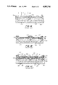
- FIGS. 1(a)-(c) illustrate the steps in a conventional method for producing a conventional polycide gate.
- a P well region 102 and an N well region 103 are formed in substrate 101.
- Boron ions, B + are injected in low concentration into the N well region as illustrated by arrows 106, in order to regulate the threshold voltage of the P channel region.
- FIG. 1(b) shows photoetching of a gate oxide layer 107 necessitated by the formation of the N channel region by contact self-alignment. Subsequently, a polysilicon layer 109 is deposited and N type impurities are thermally diffused resulting in formation of an N plus diffusion region 108 by contact self-alignment. A molybdenum disilicon MoSi 2 layer 110 is formed on the polysilicon layer 109 by sputtering.
- FIG. 1(c) shows photoetching of the polycide layer formed of silicide layer 110 over polysilicon layer 109.
- the entire polycide layer is etched with the exception of the portions that are to become gate electrodes and transmission lines from diffusion layer 108.
- Boron ions B + are injected into P well region 102 and phosphorus ions P + are injected into N well region 103.
- source and drain regions 111 and 112, respectively, are formed in each channel.
- a layer of phosphoric silicate glass (PSG) 113 is deposited across the structure.
- contact holes for connecting the diffusion regions and transmission lines are formed by etching PSG 113.
- an aluminum silicon connector 114 is deposited in the contact holes.
- PSG phosphoric silicate glass
- the P channel is not formed by contact self-alignment.
- the punch through voltage falls as the result of the injection of boron ions into the P channel to regulate the threshold voltage.
- the P channel In order to maintain satisfactory performance it is necessary to make the P channel about 0.5 u longer than the N channel.
- FIGS. 2(a)-(c) shows cross-sectional views of a semiconductor device manufactured in accordance with the process of the invention.
- a P well region 202 and an N well region 203 are formed in a substrate 201.
- Each active region is formed by local oxidation of silicon (Locos) 204.
- Locos regions 204 are an insulating layer for isolating adjacent elements.
- a gate insulating film 205 is formed over P well region 202 and N well region 203.
- an N type polysilicon layer 207 is formed on P well region 202 and a P type polysilicon layer 208 is formed on N well region 203. Since both the P and the N channels are formed by contact self-alignment, it is not necessary to inject boron ions, B + , into the P channel for regulating the threshold voltage.
- Gate insulating film 205 is formed by photoetching.
- P+ and N+ diffusion regions 210 and 209, respectively, are formed by thermal diffusion utilizing gate oxide layer 205 for contact self-alignment.
- a tungsten disilicon WSi 2 layer 211 is formed on the structure by sputtering.
- WSi 2 silicide layer 211 and polysilicon layers 207 and 208 are photoetched except for the portions in the region that are to become gate electrodes and transmission lines from diffusion regions.
- Arsenic ions As are injected into P well region 202 and boron difluoride BF 2 ions are injected into N well region 203 in order to form a source and a drain region 213 and 214, respectively, in each well region.
- a layer of phosphoric silicate glass (PSG) 215 is deposited across the device and contact holes 217 are formed by etching PSG layer 215. Contact holes are used to connect the diffusion regions and the transmission line.
- an aluminum connector 216 is formed to connect to the source or drain regions through contact holes 217.
- both the P and N channel regions are formed by contact self-alignment. Furthermore, since the silicide layer is deposited at an upper portion, it is possible to connect the P and N diffusion regions directly to the adjacent transistor through the silicide wiring. Accordingly, the variety of available pattern designs increases, thereby resulting in reduction of the total size of the semiconductor device. Processes of predeposition and ion injection are available for forming the P type or the N type polysilicon layers. Particularly if source and drain regions are formed by diffusion simultaneously with the formation of the N type and P type polysilicon layers, the manufacturing process is improved significantly over manufacturing processes available in the prior art.
- FIG. 3 illustrates an application of the process of the present invention to a salicide, or self-aligned silicide, structure.
- a P well region 302 and an N well region 303 are formed in a substrate 301. Each active region is formed by local oxidation of silicon with adjacent elements isolated by locos 304.
- Polysilicon is deposited and a polysilicon gate 306 is formed by photoetching. Using polysilicon gates 306 as a mask, low concentration diffusion layers 307 and 308 are formed in order to prevent the generation of hot electrons.
- Boron fluoride ions BF +2 are injected into N well region 303 at an energy level of 60 KeV to a density of 1 ⁇ 10 13 per square centimeter.
- P well region 302 phosphorus ions P + are injected into P well region 302 at an energy of 40 KeV to a density of 2 ⁇ 10 13 per square centimeter.
- Polysilicon P and N channel gates 306 are not doped. P type and N type polysilicon gates 306 could also be formed by diffusion of boron into N well region 303 and phosphorus into P well region 302.
- an Si0 2 film having a thickness of 6000 A is deposited on the structure and Si0 2 sidewalls 309 are formed on the sides of polysilicon gate 306 by reactive ion etching.
- a titanium Ti layer 310 having a thickness of 500 A is deposited across the device and a titanium disilicon TiSi 2 layer 311 is formed at the exposed silicon regions by lamp annealing at a temperature of between about 600° and 800° C.
- Ti layer 310 is removed everywhere except the exposed silicon regions by ammonia and water, i.e. NH 4 0H+H 2 0+H 2 0, series etching solution to provide a salicide structure.
- Boron ions, 11 B + are injected into N well region 303 at an energy of between about 40 and 120 KeV to a density of 6 ⁇ 10 15 per square centimeter and phosphorus ions, 31 P + , are injected into P well region 302 at an energy of between about 60 and 150 KeV to a density of 8 ⁇ 10 15 per square centimeter.
- a phosphoric silicate glass (PSG) film 316 having a thickness of 6000 A is deposited across the device and is annealed with a lamp for approximately 6 seconds at a temperature between about 1000° and 1050° C. in order to activate the ions and form P-N junctions beneath TiSi 2 layer 311 at the source and drain regions. Since the gate regions are formed of TiSi 2 layer 311 over non-doped Si0 2 , boron ions, B + , penetrate into TiSi 2 layer 311 and are diffused into the non-doped silicon to form the P type polysilicon gate on the side of the P channel regions. Similarly, an N type polysilicon gate is formed over the N channel regions. Contact holes 318 for connecting the diffusion regions and the transmission line is formed by etching PSG layer 316. Finally, an aluminum Al connector 317 is deposited into contact holes 316.
- PSG phosphoric silicate glass
- low resistance P and N type gates and a low resistance P-N junction can be formed simultaneously by a single injection of ions into the P and N channel regions. Furthermore, when a contact self-alignment process of the type described in Example 2 is used, P type and N type regions in the self-aligned portion are connected simultaneously and have low resistance. In this manner, the manufacturing process is reduced and high speed operation and high density integration for VLSI devices are realized.
- short channel effect is reduced in both the P and the N channel regions and, simultaneously, the resistance of the source, gate and drain is raised.
- a contact self-alignment process is not employed, although such a process would be practical. Accordingly, a semiconductor device in which P and N channels are formed by contact self-alignment is provided and short channel effect is reduced. Such improvements are not realized in conventional structures using polycide and silicide gates.
Landscapes
- Engineering & Computer Science (AREA)
- Power Engineering (AREA)
- Physics & Mathematics (AREA)
- Condensed Matter Physics & Semiconductors (AREA)
- General Physics & Mathematics (AREA)
- Computer Hardware Design (AREA)
- Microelectronics & Electronic Packaging (AREA)
- Manufacturing & Machinery (AREA)
- Metal-Oxide And Bipolar Metal-Oxide Semiconductor Integrated Circuits (AREA)
- Insulated Gate Type Field-Effect Transistor (AREA)
- Electrodes Of Semiconductors (AREA)
Abstract
A novel semiconductor device and method of production of such a device are provided. Both the N and P channels of the novel semiconductor device are formed by contact self-alignment, thereby permitting high speed operation and high density integration to be realized. The formation of the channels by contact self-alignment is accomplished by depositing a P type polysilicon layer on an N well region and an N type polysilicon layer on a P well region. A silicide layer if formed over both the P and N type polysilicon layers to form a polycide.
Description
This is a continuation of application Ser. No. 06,807,408, filed Dec. 10, 1985, now abandoned.
The invention relates to semiconductor devices and, in particular, to semiconductor devices in which short channel effects are minimized.
Recently, techniques for lowering the resistance of gate, source and drain regions have been necessary for the high speed operation of very large scale integration (VLSI) devices. Polycide structures for use as gate portions and salicide structures for lowering the resistance of the gate, source and drain regions have been developed. However, in general, polysilicon beneath silicide is of the N+ type only and connection with the substrate is accomplished only on the N channel side.
Since the polycide consists of two layers, even though polysilicon beneath silicide is provided on both P and N channel regions having different polarities, the P and N channels are connected at the upper silicide. Furthermore, when the P and N channels are simultaneously formed by contact self-alignment, it is possible to connect the drain regions of the P and N channels to adjacent transistors. It, therefore, becomes possible to lower the resistance of the gate, source and drain of the P and N channels and the process of connecting the regions, that is, providing aluminum on the contact portion of the polysilicon between the different polarities of the P and N channel regions, is reduced.
In order to reduce resistor/capacitor, RC delay in gate wiring, conventional N+ polysilicon gate materials have been replaced by silicide, polycide and refractory metals. In conventional polycide gates, the P channel is not formed by contact self-alignment because the polysilicon contains N type impurities. It has been necessary to inject boron ions, B+, into the P channel in order to decrease the differences in work function between the P and N channels and regulate threshold voltage. However, injection of boron ions causes punch through voltage to fall.
It is, therefore, desirable to provide a novel semiconductor device in which both the P and N channels are formed by contact self-alignment and which overcomes the defects of prior art semiconductor devices.
Generally speaking, in accordance with the invention a novel semiconductor device and method of making such a device are provided. Both the N and P channels of the novel semiconductor device are formed by contact self-alignment, thereby permitting high speed operation and high density integration to be realized.
Accordingly, it is an object of the invention to provide an improved semiconductor device and method of fabrication.
It is another object of the present invention to provide a semiconductor device wherein the P and N channels are formed by contact self-alignment.
It is a further object of the invention to provide a method for making the semiconductor device including forming both the N and P channels by contact self-alignment.
Still other objects and advantages of the invention will in part be obvious and will in part be apparent from the specification.
The invention accordingly comprises the several steps and the relation of one or more such steps with respect to each of the others, and the article possessing the features, properties and the relation of elements, which are exemplified in the following detailed disclosure, and the scope of the invention will be indicated in the claims.
For a fuller understanding of the invention, reference is had to the following description taken in connection with the accompanying drawings, in which:
FIGS. 1(a)-(c) are cross-sectional views showing the steps in a conventional method for producing a semiconductor device including a conventional polycide gate;
FIGS. 2(a)-(c) are cross-sectional views showing the steps in a method for forming a CMOS integrated circuit including a polycide gate prepared in accordance with the invention; and
FIGS. 3(a)-(d) are cross-sectional views showing the steps in a method for forming a CMOS integrated circuit using a silicide gate formed in accordance with the invention.
A semiconductor device and a method for producing such device in which both the P and the N channels are formed by contact self-alignment are provided. This is accomplished by depositing a P type polysilicon layer on an N well region and an N type polysilicon layer on a P well region. A metal disilicon, MSi2 or silicide layer is formed over both the P and N type polysilicon layers to form a polycide.
By providing a P type polysilicon layer over the N well region and an N type polysilicon layer over the P well region, both P and N channels can be formed simultaneously by contact self-alignment. Drain regions of P and N channels of adjacent transistors can be connected. This permits reduction in resistance of the gate, source and drain regions and an increase in the punch through voltage. Furthermore, the method for producing the device is improved, short channel effect is decreased, the variety of pattern designs increases and high integration is realized.
For a better understanding of the semiconductor devices constructed in accordance with the invention, and the methods of construction, reference is made to the following examples. These examples are presented for purposes of illustration only and are not intended to be construed in a limiting sense.
FIGS. 1(a)-(c) illustrate the steps in a conventional method for producing a conventional polycide gate. In FIG. 1(a), a P well region 102 and an N well region 103 are formed in substrate 101. Boron ions, B+, are injected in low concentration into the N well region as illustrated by arrows 106, in order to regulate the threshold voltage of the P channel region.
FIG. 1(b) shows photoetching of a gate oxide layer 107 necessitated by the formation of the N channel region by contact self-alignment. Subsequently, a polysilicon layer 109 is deposited and N type impurities are thermally diffused resulting in formation of an N plus diffusion region 108 by contact self-alignment. A molybdenum disilicon MoSi2 layer 110 is formed on the polysilicon layer 109 by sputtering.
FIG. 1(c) shows photoetching of the polycide layer formed of silicide layer 110 over polysilicon layer 109. The entire polycide layer is etched with the exception of the portions that are to become gate electrodes and transmission lines from diffusion layer 108. Boron ions B+ are injected into P well region 102 and phosphorus ions P+ are injected into N well region 103. In this manner, source and drain regions 111 and 112, respectively, are formed in each channel. A layer of phosphoric silicate glass (PSG) 113 is deposited across the structure. Then contact holes for connecting the diffusion regions and transmission lines are formed by etching PSG 113. Finally, an aluminum silicon connector 114 is deposited in the contact holes.
In this conventional method, the P channel is not formed by contact self-alignment. The punch through voltage falls as the result of the injection of boron ions into the P channel to regulate the threshold voltage. In order to maintain satisfactory performance it is necessary to make the P channel about 0.5 u longer than the N channel.
FIGS. 2(a)-(c) shows cross-sectional views of a semiconductor device manufactured in accordance with the process of the invention. Referring to FIG. 2(a), a P well region 202 and an N well region 203 are formed in a substrate 201. Each active region is formed by local oxidation of silicon (Locos) 204. Locos regions 204 are an insulating layer for isolating adjacent elements. A gate insulating film 205 is formed over P well region 202 and N well region 203.
Referring to FIG. 2(b), an N type polysilicon layer 207 is formed on P well region 202 and a P type polysilicon layer 208 is formed on N well region 203. Since both the P and the N channels are formed by contact self-alignment, it is not necessary to inject boron ions, B+, into the P channel for regulating the threshold voltage. Gate insulating film 205 is formed by photoetching. P+ and N+ diffusion regions 210 and 209, respectively, are formed by thermal diffusion utilizing gate oxide layer 205 for contact self-alignment. A tungsten disilicon WSi2 layer 211 is formed on the structure by sputtering.
Referring to FIG. 2(c), WSi2 silicide layer 211 and polysilicon layers 207 and 208 are photoetched except for the portions in the region that are to become gate electrodes and transmission lines from diffusion regions. Arsenic ions As are injected into P well region 202 and boron difluoride BF2 ions are injected into N well region 203 in order to form a source and a drain region 213 and 214, respectively, in each well region. A layer of phosphoric silicate glass (PSG) 215 is deposited across the device and contact holes 217 are formed by etching PSG layer 215. Contact holes are used to connect the diffusion regions and the transmission line. Finally, an aluminum connector 216 is formed to connect to the source or drain regions through contact holes 217.
In accordance with the invention, both the P and N channel regions are formed by contact self-alignment. Furthermore, since the silicide layer is deposited at an upper portion, it is possible to connect the P and N diffusion regions directly to the adjacent transistor through the silicide wiring. Accordingly, the variety of available pattern designs increases, thereby resulting in reduction of the total size of the semiconductor device. Processes of predeposition and ion injection are available for forming the P type or the N type polysilicon layers. Particularly if source and drain regions are formed by diffusion simultaneously with the formation of the N type and P type polysilicon layers, the manufacturing process is improved significantly over manufacturing processes available in the prior art.
FIG. 3 illustrates an application of the process of the present invention to a salicide, or self-aligned silicide, structure. A P well region 302 and an N well region 303 are formed in a substrate 301. Each active region is formed by local oxidation of silicon with adjacent elements isolated by locos 304. Polysilicon is deposited and a polysilicon gate 306 is formed by photoetching. Using polysilicon gates 306 as a mask, low concentration diffusion layers 307 and 308 are formed in order to prevent the generation of hot electrons. Boron fluoride ions BF+2 are injected into N well region 303 at an energy level of 60 KeV to a density of 1×10¹³ per square centimeter. Similarly, phosphorus ions P+ are injected into P well region 302 at an energy of 40 KeV to a density of 2×10¹³ per square centimeter. Polysilicon P and N channel gates 306 are not doped. P type and N type polysilicon gates 306 could also be formed by diffusion of boron into N well region 303 and phosphorus into P well region 302.
Referring to FIG. 3(b), an Si02 film having a thickness of 6000 A is deposited on the structure and Si02 sidewalls 309 are formed on the sides of polysilicon gate 306 by reactive ion etching. A titanium Ti layer 310 having a thickness of 500 A is deposited across the device and a titanium disilicon TiSi2 layer 311 is formed at the exposed silicon regions by lamp annealing at a temperature of between about 600° and 800° C.
Referring to FIG. 3(c), Ti layer 310 is removed everywhere except the exposed silicon regions by ammonia and water, i.e. NH4 0H+H2 0+H2 0, series etching solution to provide a salicide structure. Boron ions, 11 B+, are injected into N well region 303 at an energy of between about 40 and 120 KeV to a density of 6×10¹⁵ per square centimeter and phosphorus ions, 31 P+, are injected into P well region 302 at an energy of between about 60 and 150 KeV to a density of 8×10¹⁵ per square centimeter.
Referring to FIG. 3(d), a phosphoric silicate glass (PSG) film 316 having a thickness of 6000 A is deposited across the device and is annealed with a lamp for approximately 6 seconds at a temperature between about 1000° and 1050° C. in order to activate the ions and form P-N junctions beneath TiSi2 layer 311 at the source and drain regions. Since the gate regions are formed of TiSi2 layer 311 over non-doped Si02, boron ions, B+, penetrate into TiSi2 layer 311 and are diffused into the non-doped silicon to form the P type polysilicon gate on the side of the P channel regions. Similarly, an N type polysilicon gate is formed over the N channel regions. Contact holes 318 for connecting the diffusion regions and the transmission line is formed by etching PSG layer 316. Finally, an aluminum Al connector 317 is deposited into contact holes 316.
In accordance with this embodiment of the invention, low resistance P and N type gates and a low resistance P-N junction can be formed simultaneously by a single injection of ions into the P and N channel regions. Furthermore, when a contact self-alignment process of the type described in Example 2 is used, P type and N type regions in the self-aligned portion are connected simultaneously and have low resistance. In this manner, the manufacturing process is reduced and high speed operation and high density integration for VLSI devices are realized.
According to the method in accordance with the invention, short channel effect is reduced in both the P and the N channel regions and, simultaneously, the resistance of the source, gate and drain is raised. In this embodiment of the invention, a contact self-alignment process is not employed, although such a process would be practical. Accordingly, a semiconductor device in which P and N channels are formed by contact self-alignment is provided and short channel effect is reduced. Such improvements are not realized in conventional structures using polycide and silicide gates.
It will thus be seen that the objects set forth above, among those made apparent from the preceding description, are efficiently attained and, since certain changes may be made in carrying out the above method and in the article set forth without departing from the spirit and scope of the invention, it is intended that all matter contained in the above description and shown in the accompanying drawings shall be interpreted as illustrative and not in a limiting sense.
It is also to be understood that the following claims are intended to cover all of the generic and specific features of the invention herein described and all statements of the scope of the invention which, as a matter of language, might be said to fall therebetween.
Claims (12)
1. A semiconductor device comprising:
a substrate of a first conductivity type;
a well region of a second conductivity type formed in said substrate;
a first gate insulating film provided on a portion of said well region;
a first polycrystalline silicon gate of the first conductivity type formed on the first gate insulating film;
a second gate insulating film provided on a portion of said substrate;
a second polycrystalline silicon gate of the second conductivity type formed on the second gate insulating film;
first source and drain regions provided in the well region on either side of the first polycrystalline silicon gate;
first polycrystalline silicon wiring of the first conductivity type drawn from the first drain region;
second source and drain regions provided in the substrate on either side of the second polycrystalline silicon gate;
second polycrystalline silicon wiring of the second conductivity type drawn from the second drain region, said wiring of said first conductive type drawn from the first drain region being directly connected to the wiring of the second conductive type; and
a metal silicide film formed on substantially the entire surfaces of the polycrystalline silicon wiring and the polycrystalline silicon gates without contacting the source or drain regions.
2. The semiconductor device of claim 1, wherein a well region of a first conductive type is formed in said substrate and wherein said second gate insulating film is formed on said well region of said first conductive type.
3. The semiconductor device of claim 1, wherein the metal silicide film is selected from the group consisting of molybdenum disilicon (MoSi2), tungsten disilicon (WSi2) and titanium disilicon (TiSi2).
4. The semiconductor device of claim 1, wherein the first drain region includes a first drain diffusion region along one side thereof and the second drain region includes a second drain diffusion region along one side thereof and the first drain diffusion region is separated from the second drain diffusion region by an element isolating region.
5. The semiconductor device of claim 4, wherein the first drain diffusion region is the first conductivity type and the second drain diffusion region is the second conductivity type.
6. The semiconductor device of claim 4, wherein the first polycrystalline silicon wiring is directly connected to the second polycrystalline silicon wiring on the surface of the element isolating region.
7. The semiconductor device of claim 4, wherein at least one of the source and drain regions extends under an end of a polycrystalline silicon gate along one side thereof and is in contact with an element isolating region along the opposite side thereof.
8. The semiconductor device of claim 1, further including an insulating material provided as a side wall of each of the gate electrodes.
9. The semiconductor device of claim 1, wherein each of the drain regions includes a low density drain region and a high density drain region and each of the source regions includes a low density source region and a high density source region.
10. The semiconductor device of claim 9, wherein the low density source and drain regions are thin and are adjacent a gate electrode and the high density source and drain regions have a thickness greater than the thickness of the low density regions and are distal from the gate electrode.
11. The semiconductor device of claim 8, wherein each of the drain regions includes a low density drain region and a high density drain region and each of the source regions includes a low density source region and a high density source region.
12. The semiconductor device of claim 11, wherein the low density source and drain regions are provided under the side wall of the gate electrode.
Priority Applications (1)
| Application Number | Priority Date | Filing Date | Title |
|---|---|---|---|
| US07/916,800 US5190886A (en) | 1984-12-11 | 1992-07-17 | Semiconductor device and method of production |
Applications Claiming Priority (2)
| Application Number | Priority Date | Filing Date | Title |
|---|---|---|---|
| JP59-261251 | 1984-12-11 | ||
| JP59261251A JPS61139058A (en) | 1984-12-11 | 1984-12-11 | Production apparatus for semiconductor |
Related Parent Applications (1)
| Application Number | Title | Priority Date | Filing Date |
|---|---|---|---|
| US80740885A Continuation | 1984-12-11 | 1985-12-10 |
Related Child Applications (1)
| Application Number | Title | Priority Date | Filing Date |
|---|---|---|---|
| US55328190A Division | 1984-12-11 | 1990-07-17 |
Publications (1)
| Publication Number | Publication Date |
|---|---|
| US4985746A true US4985746A (en) | 1991-01-15 |
Family
ID=17359228
Family Applications (3)
| Application Number | Title | Priority Date | Filing Date |
|---|---|---|---|
| US07/075,245 Expired - Lifetime US4985746A (en) | 1984-12-11 | 1987-07-16 | Semiconductor device and method of production |
| US07/698,048 Expired - Lifetime US5086006A (en) | 1984-12-11 | 1991-05-10 | Semiconductor device and method of production |
| US07/702,134 Expired - Lifetime US5093276A (en) | 1984-12-11 | 1991-05-13 | Semiconductor device and method of production |
Family Applications After (2)
| Application Number | Title | Priority Date | Filing Date |
|---|---|---|---|
| US07/698,048 Expired - Lifetime US5086006A (en) | 1984-12-11 | 1991-05-10 | Semiconductor device and method of production |
| US07/702,134 Expired - Lifetime US5093276A (en) | 1984-12-11 | 1991-05-13 | Semiconductor device and method of production |
Country Status (2)
| Country | Link |
|---|---|
| US (3) | US4985746A (en) |
| JP (1) | JPS61139058A (en) |
Cited By (10)
| Publication number | Priority date | Publication date | Assignee | Title |
|---|---|---|---|---|
| AU640475B2 (en) * | 1990-06-01 | 1993-08-26 | Minnesota Mining And Manufacturing Company | Stack of sheet assemblies |
| US5278082A (en) * | 1992-04-03 | 1994-01-11 | Sharp Kabushiki Kaisha | Method for electrically connecting an electrode and impurity-diffused layer formed on a semiconductor substrate |
| US5280190A (en) * | 1991-03-21 | 1994-01-18 | Industrial Technology Research Institute | Self aligned emitter/runner integrated circuit |
| US5300797A (en) * | 1992-03-31 | 1994-04-05 | Sgs-Thomson Microelectronics, Inc. | Coplanar twin-well integrated circuit structure |
| US5341014A (en) * | 1992-01-07 | 1994-08-23 | Matsushita Electric Industrial Co., Ltd. | Semiconductor device and a method of fabricating the same |
| US5355010A (en) * | 1991-06-21 | 1994-10-11 | Matsushita Electric Industrial Co., Ltd. | Semiconductor device with a dual type polycide layer comprising a uniformly p-type doped silicide |
| US5478771A (en) * | 1993-05-28 | 1995-12-26 | Sgs-Thomson Microelectronics, Inc. | Method of forming local interconnect structure without P-N junction between active elements |
| US5589415A (en) * | 1995-06-07 | 1996-12-31 | Sgs-Thomson Microelectronics, Inc. | Method for forming a semiconductor structure with self-aligned contacts |
| US6388296B1 (en) * | 1998-06-04 | 2002-05-14 | Sharp Laboratories Of America, Inc. | CMOS self-aligned strapped interconnection |
| US6545328B1 (en) * | 1999-04-15 | 2003-04-08 | Sharp Kabushiki Kaisha | Semiconductor device |
Families Citing this family (9)
| Publication number | Priority date | Publication date | Assignee | Title |
|---|---|---|---|---|
| US5247199A (en) * | 1986-01-15 | 1993-09-21 | Harris Corporation | Process for forming twin well CMOS integrated circuits |
| US5418179A (en) * | 1988-05-31 | 1995-05-23 | Yamaha Corporation | Process of fabricating complementary inverter circuit having multi-level interconnection |
| JP2845899B2 (en) * | 1988-08-24 | 1999-01-13 | 株式会社日立製作所 | Method for manufacturing semiconductor integrated circuit device |
| JPH0758701B2 (en) * | 1989-06-08 | 1995-06-21 | 株式会社東芝 | Method for manufacturing semiconductor device |
| US5274261A (en) * | 1990-07-31 | 1993-12-28 | Texas Instruments Incorporated | Integrated circuit degradation resistant structure |
| JP2901788B2 (en) * | 1991-07-19 | 1999-06-07 | ローム株式会社 | Silicon carbide semiconductor device |
| US5409847A (en) * | 1993-10-27 | 1995-04-25 | Matsushita Electric Industrial Co., Ltd. | Manufacturing method of CMOS transistor in which heat treatment at higher temperature is done prior to heat treatment at low temperature |
| US5489797A (en) * | 1994-12-19 | 1996-02-06 | Sgs-Thomson Microelectronics, Inc. | Local interconnect structure |
| DE19510777C1 (en) * | 1995-03-24 | 1996-06-05 | Itt Ind Gmbh Deutsche | Process for producing a CMOS structure with ESD protection |
Citations (3)
| Publication number | Priority date | Publication date | Assignee | Title |
|---|---|---|---|---|
| US4333099A (en) * | 1978-02-27 | 1982-06-01 | Rca Corporation | Use of silicide to bridge unwanted polycrystalline silicon P-N junction |
| US4476482A (en) * | 1981-05-29 | 1984-10-09 | Texas Instruments Incorporated | Silicide contacts for CMOS devices |
| US4477310A (en) * | 1983-08-12 | 1984-10-16 | Tektronix, Inc. | Process for manufacturing MOS integrated circuit with improved method of forming refractory metal silicide areas |
Family Cites Families (24)
| Publication number | Priority date | Publication date | Assignee | Title |
|---|---|---|---|---|
| JPS54150090A (en) * | 1978-05-17 | 1979-11-24 | Matsushita Electric Ind Co Ltd | Manufacture of semiconductor device |
| JPS5583264A (en) * | 1978-12-19 | 1980-06-23 | Fujitsu Ltd | Method of fabricating mos semiconductor device |
| JPS5660063A (en) * | 1979-10-23 | 1981-05-23 | Chiyou Lsi Gijutsu Kenkyu Kumiai | Manufacture of semiconductor device |
| JPS56124270A (en) * | 1980-03-05 | 1981-09-29 | Hitachi Ltd | Manufacture of semiconductor device |
| US4382827A (en) * | 1981-04-27 | 1983-05-10 | Ncr Corporation | Silicon nitride S/D ion implant mask in CMOS device fabrication |
| US4374700A (en) * | 1981-05-29 | 1983-02-22 | Texas Instruments Incorporated | Method of manufacturing silicide contacts for CMOS devices |
| JPS5810868A (en) * | 1981-07-13 | 1983-01-21 | Sanyo Electric Co Ltd | Manufacture of complementary insulting gate type field effect semiconductor device |
| DE3132809A1 (en) * | 1981-08-19 | 1983-03-10 | Siemens AG, 1000 Berlin und 8000 München | METHOD FOR PRODUCING INTEGRATED MOS FIELD EFFECT TRANSISTORS, ESPECIALLY COMPLEMENTARY MOS FIELD EFFECT TRANSISTOR CIRCUITS WITH AN ADDITIONAL CIRCUIT LEVEL CONSTRUCTED FROM METAL SILICIDES |
| US4432132A (en) * | 1981-12-07 | 1984-02-21 | Bell Telephone Laboratories, Incorporated | Formation of sidewall oxide layers by reactive oxygen ion etching to define submicron features |
| US4613885A (en) * | 1982-02-01 | 1986-09-23 | Texas Instruments Incorporated | High-voltage CMOS process |
| JPS58175846A (en) * | 1982-04-08 | 1983-10-15 | Toshiba Corp | Manufacture of semicondutor device |
| JPS593918A (en) * | 1982-06-29 | 1984-01-10 | Toshiba Corp | Manufacture of complementary semiconductor device |
| JPS59208772A (en) * | 1983-05-12 | 1984-11-27 | Nec Corp | Manufacture of semiconductor device |
| JPS6017943A (en) * | 1983-07-08 | 1985-01-29 | Matsushita Electronics Corp | Manufacture of semiconductor device |
| JPS6017946A (en) * | 1983-07-12 | 1985-01-29 | Seiko Epson Corp | Semiconductor device |
| JPS6059771A (en) * | 1983-09-13 | 1985-04-06 | Toshiba Corp | Semiconductor device and manufacture thereof |
| US4546535A (en) * | 1983-12-12 | 1985-10-15 | International Business Machines Corporation | Method of making submicron FET structure |
| IT1213120B (en) * | 1984-01-10 | 1989-12-14 | Ates Componenti Elettron | PROCESS FOR THE MANUFACTURE OF COMPLEMENTARY LOW VOLTAGE THRESHOLD MOS TRANSISTORS IN HIGH DENSITY INTEGRATED CIRCUITS AND RESULTING STRUCTURE. |
| FR2562327B1 (en) * | 1984-03-30 | 1986-06-20 | Commissariat Energie Atomique | METHOD FOR INTERCONNECTING ACTIVE ZONES AND / OR GRIDS OF INTEGRATED CMOS CIRCUITS |
| JPS615580A (en) * | 1984-06-19 | 1986-01-11 | Toshiba Corp | Manufacture of semiconductor device |
| US4577391A (en) * | 1984-07-27 | 1986-03-25 | Monolithic Memories, Inc. | Method of manufacturing CMOS devices |
| US4621412A (en) * | 1984-09-17 | 1986-11-11 | Sony Corporation | Manufacturing a complementary MOSFET |
| US4639274A (en) * | 1984-11-28 | 1987-01-27 | Fairchild Semiconductor Corporation | Method of making precision high-value MOS capacitors |
| US4654958A (en) * | 1985-02-11 | 1987-04-07 | Intel Corporation | Process for forming isolated silicon regions and field-effect devices on a silicon substrate |
-
1984
- 1984-12-11 JP JP59261251A patent/JPS61139058A/en active Pending
-
1987
- 1987-07-16 US US07/075,245 patent/US4985746A/en not_active Expired - Lifetime
-
1991
- 1991-05-10 US US07/698,048 patent/US5086006A/en not_active Expired - Lifetime
- 1991-05-13 US US07/702,134 patent/US5093276A/en not_active Expired - Lifetime
Patent Citations (3)
| Publication number | Priority date | Publication date | Assignee | Title |
|---|---|---|---|---|
| US4333099A (en) * | 1978-02-27 | 1982-06-01 | Rca Corporation | Use of silicide to bridge unwanted polycrystalline silicon P-N junction |
| US4476482A (en) * | 1981-05-29 | 1984-10-09 | Texas Instruments Incorporated | Silicide contacts for CMOS devices |
| US4477310A (en) * | 1983-08-12 | 1984-10-16 | Tektronix, Inc. | Process for manufacturing MOS integrated circuit with improved method of forming refractory metal silicide areas |
Cited By (13)
| Publication number | Priority date | Publication date | Assignee | Title |
|---|---|---|---|---|
| AU640475B2 (en) * | 1990-06-01 | 1993-08-26 | Minnesota Mining And Manufacturing Company | Stack of sheet assemblies |
| US5280190A (en) * | 1991-03-21 | 1994-01-18 | Industrial Technology Research Institute | Self aligned emitter/runner integrated circuit |
| US5355010A (en) * | 1991-06-21 | 1994-10-11 | Matsushita Electric Industrial Co., Ltd. | Semiconductor device with a dual type polycide layer comprising a uniformly p-type doped silicide |
| US5459101A (en) * | 1991-06-21 | 1995-10-17 | Matsushita Electric Industrial Co., Ltd. | Method for fabricating a semiconductor device comprising a polycide structure |
| US5341014A (en) * | 1992-01-07 | 1994-08-23 | Matsushita Electric Industrial Co., Ltd. | Semiconductor device and a method of fabricating the same |
| US5300797A (en) * | 1992-03-31 | 1994-04-05 | Sgs-Thomson Microelectronics, Inc. | Coplanar twin-well integrated circuit structure |
| US5278082A (en) * | 1992-04-03 | 1994-01-11 | Sharp Kabushiki Kaisha | Method for electrically connecting an electrode and impurity-diffused layer formed on a semiconductor substrate |
| US5478771A (en) * | 1993-05-28 | 1995-12-26 | Sgs-Thomson Microelectronics, Inc. | Method of forming local interconnect structure without P-N junction between active elements |
| US5670424A (en) * | 1993-05-28 | 1997-09-23 | Sgs-Thomson Microelectronics, Inc. | Method for making local interconnect structure |
| US5589415A (en) * | 1995-06-07 | 1996-12-31 | Sgs-Thomson Microelectronics, Inc. | Method for forming a semiconductor structure with self-aligned contacts |
| US5640037A (en) * | 1995-06-07 | 1997-06-17 | Sgs-Thomson Microelectronics, Inc. | Cell with self-aligned contacts |
| US6388296B1 (en) * | 1998-06-04 | 2002-05-14 | Sharp Laboratories Of America, Inc. | CMOS self-aligned strapped interconnection |
| US6545328B1 (en) * | 1999-04-15 | 2003-04-08 | Sharp Kabushiki Kaisha | Semiconductor device |
Also Published As
| Publication number | Publication date |
|---|---|
| US5086006A (en) | 1992-02-04 |
| JPS61139058A (en) | 1986-06-26 |
| US5093276A (en) | 1992-03-03 |
Similar Documents
| Publication | Publication Date | Title |
|---|---|---|
| US4985746A (en) | Semiconductor device and method of production | |
| US4392150A (en) | MOS Integrated circuit having refractory metal or metal silicide interconnect layer | |
| US4329706A (en) | Doped polysilicon silicide semiconductor integrated circuit interconnections | |
| US5175118A (en) | Multiple layer electrode structure for semiconductor device and method of manufacturing thereof | |
| US4312680A (en) | Method of manufacturing submicron channel transistors | |
| US4701423A (en) | Totally self-aligned CMOS process | |
| US4603468A (en) | Method for source/drain self-alignment in stacked CMOS | |
| KR900008207B1 (en) | Semiconductor memory device | |
| US4992391A (en) | Process for fabricating a control gate for a floating gate FET | |
| US4373249A (en) | Method of manufacturing a semiconductor integrated circuit device | |
| US5468662A (en) | Method of making thin film transistor and a silicide local interconnect | |
| US5688722A (en) | CMOS integrated circuit with reduced susceptibility to PMOS punchthrough | |
| US4945070A (en) | Method of making cmos with shallow source and drain junctions | |
| US4637124A (en) | Process for fabricating semiconductor integrated circuit device | |
| US4519126A (en) | Method of fabricating high speed CMOS devices | |
| US4978637A (en) | Local interconnect process for integrated circuits | |
| US4743564A (en) | Method for manufacturing a complementary MOS type semiconductor device | |
| US4364166A (en) | Semiconductor integrated circuit interconnections | |
| US4901134A (en) | Semiconductor device and manufacturing method thereof | |
| US5190886A (en) | Semiconductor device and method of production | |
| US5079617A (en) | Multiple layer electrode structure for semiconductor device and method of manufacturing thereof | |
| US5045966A (en) | Method for forming capacitor using FET process and structure formed by same | |
| EP0187260B1 (en) | Process for fabricating a semiconductor integrated circuit device having misfets | |
| US4517731A (en) | Double polysilicon process for fabricating CMOS integrated circuits | |
| US5960303A (en) | Process of forming titanium silicide interconnects |
Legal Events
| Date | Code | Title | Description |
|---|---|---|---|
| STCF | Information on status: patent grant |
Free format text: PATENTED CASE |
|
| FEPP | Fee payment procedure |
Free format text: PAYOR NUMBER ASSIGNED (ORIGINAL EVENT CODE: ASPN); ENTITY STATUS OF PATENT OWNER: LARGE ENTITY |
|
| FPAY | Fee payment |
Year of fee payment: 4 |
|
| FPAY | Fee payment |
Year of fee payment: 8 |
|
| FPAY | Fee payment |
Year of fee payment: 12 |