EP0427260B1 - Dispositif de mémoires non-volatiles - Google Patents
Dispositif de mémoires non-volatiles Download PDFInfo
- Publication number
- EP0427260B1 EP0427260B1 EP90121404A EP90121404A EP0427260B1 EP 0427260 B1 EP0427260 B1 EP 0427260B1 EP 90121404 A EP90121404 A EP 90121404A EP 90121404 A EP90121404 A EP 90121404A EP 0427260 B1 EP0427260 B1 EP 0427260B1
- Authority
- EP
- European Patent Office
- Prior art keywords
- bit lines
- circuit
- volatile memory
- memory cells
- word lines
- Prior art date
- Legal status (The legal status is an assumption and is not a legal conclusion. Google has not performed a legal analysis and makes no representation as to the accuracy of the status listed.)
- Expired - Lifetime
Links
Images


Classifications
-
- G—PHYSICS
- G11—INFORMATION STORAGE
- G11C—STATIC STORES
- G11C29/00—Checking stores for correct operation ; Subsequent repair; Testing stores during standby or offline operation
-
- G—PHYSICS
- G11—INFORMATION STORAGE
- G11C—STATIC STORES
- G11C16/00—Erasable programmable read-only memories
- G11C16/02—Erasable programmable read-only memories electrically programmable
- G11C16/06—Auxiliary circuits, e.g. for writing into memory
- G11C16/34—Determination of programming status, e.g. threshold voltage, overprogramming or underprogramming, retention
-
- G—PHYSICS
- G11—INFORMATION STORAGE
- G11C—STATIC STORES
- G11C16/00—Erasable programmable read-only memories
- G11C16/02—Erasable programmable read-only memories electrically programmable
- G11C16/06—Auxiliary circuits, e.g. for writing into memory
- G11C16/10—Programming or data input circuits
- G11C16/12—Programming voltage switching circuits
-
- G—PHYSICS
- G11—INFORMATION STORAGE
- G11C—STATIC STORES
- G11C16/00—Erasable programmable read-only memories
- G11C16/02—Erasable programmable read-only memories electrically programmable
- G11C16/06—Auxiliary circuits, e.g. for writing into memory
- G11C16/30—Power supply circuits
-
- G—PHYSICS
- G11—INFORMATION STORAGE
- G11C—STATIC STORES
- G11C29/00—Checking stores for correct operation ; Subsequent repair; Testing stores during standby or offline operation
- G11C29/04—Detection or location of defective memory elements, e.g. cell constructio details, timing of test signals
- G11C29/08—Functional testing, e.g. testing during refresh, power-on self testing [POST] or distributed testing
- G11C29/12—Built-in arrangements for testing, e.g. built-in self testing [BIST] or interconnection details
- G11C29/18—Address generation devices; Devices for accessing memories, e.g. details of addressing circuits
- G11C29/30—Accessing single arrays
- G11C29/34—Accessing multiple bits simultaneously
-
- G—PHYSICS
- G11—INFORMATION STORAGE
- G11C—STATIC STORES
- G11C29/00—Checking stores for correct operation ; Subsequent repair; Testing stores during standby or offline operation
- G11C29/04—Detection or location of defective memory elements, e.g. cell constructio details, timing of test signals
- G11C29/50—Marginal testing, e.g. race, voltage or current testing
-
- G—PHYSICS
- G11—INFORMATION STORAGE
- G11C—STATIC STORES
- G11C16/00—Erasable programmable read-only memories
- G11C16/02—Erasable programmable read-only memories electrically programmable
- G11C16/04—Erasable programmable read-only memories electrically programmable using variable threshold transistors, e.g. FAMOS
-
- G—PHYSICS
- G11—INFORMATION STORAGE
- G11C—STATIC STORES
- G11C29/00—Checking stores for correct operation ; Subsequent repair; Testing stores during standby or offline operation
- G11C29/70—Masking faults in memories by using spares or by reconfiguring
- G11C29/78—Masking faults in memories by using spares or by reconfiguring using programmable devices
Definitions
- the present invention relates to non-volatile memory devices, for example erasable programmable read only memories having redundant cell arrays. More particularly, the present invention is concerned with provisions for testing such memories.
- EPROM Erasable programmable read only memories
- EPROM Erasable programmable read only memories
- redundant cell arrays When a software test detects a failure in a certain bit line or word line, a cell array including the defective bit line or word line is replaced with a stand-by or redundant cell array. The address corresponding to the defective cell array is assigned to the stand-by cell array so that the EPROM can operate normally.
- the EPROM can carry out write operation and read operation for individual cells one by one in accordance with the sequence of addresses and can continue normal operation, even though a failure occurred in the defective cell array.
- a redundant cell array EPROM includes the following structure.
- a cell matrix consisting of many memory elements (for example FAMOS transistors having each a control gate and a floating gate) located at respective intersections of word lines and bit lines is structured to receive signals supplied by a plurality of address signal lines having row decoders and column decoders. The decoders select necessary cells.
- a redundant address memory circuit is provided to store addresses corresponding to each defective bit or word line in order that the defective bit line and word line may be effectively replaced. When a memory address of the redundant address memory circuit matches with information output from the column decoder and row decoder, the column decoder and row decoder are denied access to the defective memory cells and access is routed to the redundant cell arrays.
- writing of information into the cells of the EPROM is carried out for each cell in accordance with the sequence of addresses, which takes a relatively long time, due to the write characteristics of the EPROM.
- the EPROM is required to supply enough current to cells to generate avalanche breakdown, but it is not feasible to make a write circuit having sufficient current supply capability for supplying such heavy current to all cells at once. In other words, it is not feasible to simultaneously write information to all of the cells.
- the read operation is carried out in relation to individual cells in accordance with the sequence of addresses. From the viewpoint of circuit structure, it is nearly impossible to simultaneously carry out write or read operations to all cells, unless the circuit design is substantially modified.
- Fig. 1 is a diagram for assistance in explaining the general operation of an EPROM.
- a high voltage generated by a write circuit is supplied to a cell matrix through a bus line.
- Individual capacitor cells of the cell matrix are N-channel-type MOSFETs Q00 to Q1i with drains connected to bit lines BL0, BL1, ..., gates connected to word lines X0, X1, ..., Xi and sources connected to GND.
- each bit line is structured so that the desired line is selected when a transistor Q0, Q1 (a column gate) for bit line selection turns ON (Y0, Y2).
- Fig. 2 is a diagram for assistance in explaining memory cells and gives a sectional view of a capacitor cell of Fig. 1.
- a voltage VS is indicated to be applied to source region S
- a voltage VD is applied to drain region D.
- a control gate CG to which a voltage VC is applied and a floating gate FG for accumulating charges are insulated from each other and layered at the surface between the source and drain.
- the voltage VS is set to 0 volts and the voltages VC and VD are set to a high voltage (H), such as voltages VC and VD are set to a high voltage (H), such as 12.5 V.
- H high voltage
- Y0 is set to a high voltage, for example, to 5 V to turn ON the column gate Q0.
- VPP is also applied to the word line X0.
- the drain of cell Q01 is also set to VPP, the source thereof to L (OV) and the control gate CG becomes L. Therefore, an intense field is generated between the drain D and floating gate FG. If information is already written to the cell Q01 and the gate insulation film is defective, electrons are released from the floating gate FG due to the intense field and information may be permanently erased.
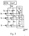
- Fig. 3 resembles the circuit of Fig. 1, but is different in that redundant bit lines (e.g. bit line BLr having cells Qr0 to Qri) are provided for replacing defective bit lines.
- the bit line BL1 is short-circuited with the GND line at the point A of such bit line BL1. As shown in Fig.
- VD VPP
- the short-circuit of the ground line to the bit line can be avoided by using a redundant bit line.
- the redundant bit line BLr is enclosed by a chain line in Fig. 3. Like the other bit lines BL0, BL1, ..., the redundant bit line BLr has a selection gate Qr and memory cells, Qr0, Qr1, ..., Qri. If the bit line BL1 is defective, a redundant bit BLr may be used in place of the bit line BL1 (Yr is set to H in place of setting Y1 to H). Thereby, if there are at least as many redundant bit lines as there are defective bit lines, it is not necessary to discard the entire memory.
- Japanese Patent No. 63-258000 discloses the concept of increasing the current supply capability of the write circuit to a sufficiently large value to compensate for a part of the current flowing into GND.
- this concept has limitations when applied to further microminiaturised memory devices because when a current higher than an allowable value flows into the microminiaturised wiring layers, the wiring layers are burned out or broken due to the generation of electromigration in which the flow of electrons pushes away the particles forming the wiring layer.
- a semiconductor non-volatile memory device having a normal operating mode and a test mode, comprising:-
- Such a semiconductor non-volatile memory device being an erasable programmable memory, wherein
- a method for testing a semiconductor non-volatile memory device having a plurality of bit lines, a plurality of word lines which intersect the bit lines, and a plurality of non-volatile memory cell transistors, each having a drain, a control gate and a source, connected to the bit lines and the word lines where the bit lines and the word lines intersect, with the drains connected to said bit lines and the control gates connected to said word lines, the sources having a connection to a ground line, characterised by the steps of:-
- Embodiments of the present invention enable the stress testing of memory devices such as the EPROM explained above in an efficient manner, even when the EPROM is using redundant bit lines because of bit line failure.
- Embodiments of the present invention enable testing to be carried out without the need to individually access each memory cell for testing.
- Embodiments of the present invention provide erasable programmable non-volatile semiconductor read only memories having redundant bit lines and word lines, and means and method for performing a stress test on all memory cells simultaneously even when a fault is generated in the cell array and redundant bit lines or word lines are used.
- An embodiment of the present invention provides an erasable programmable read only memory having a switch (Qf) inserted in the ground line.
- the switch Qf is ON in normal operation and OFF during the write stress test.
- the semiconductor memory has non-volatile memory cells which are located at respective intersecting points of a plurality of bit lines and word lines. Drains of the memory cells are connected to the bit lines, while control gates are connected to word lines. Sources are connected to the common ground line through the switch Qf. Each bit line is connected to a write circuit through a column gate, and some of the bit lines are used as redundant bit lines.
- a stress resistance test method is used to test the semiconductor memory. The switch Qf is turned OFF during the stress test so that all cells can be tested simultaneously, without problems created by short-circuits.
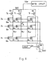
- the EPROM of Fig. 4 has redundant cell arrays.
- a cell matrix 11 has 1,048,576 capacitor cells formed by memory elements arranged at the intersecting points of word lines and bit lines.
- the matrix 11 has a row decoder 12 and column decoder 13, which receive signals supplied to address signal lines A0 - A16 to select cells.
- the circuit is provided with a redundant address memory circuit 14 for storing addresses corresponding to the defective bit (word) lines.
- a data input buffer 17 which includes a program control circuit. The program control circuit is used to write information to the device.
- the function of replacing a defective cell array with a redundant cell array is performed by assigning the address of the defective cell array to the so-called redundant cell array.
- This assignment function or procedure may be followed by a testing function or procedure in which a voltage is applied simultaneously to all cells by (1) suppressing the output of the decoder corresponding to the address of the defective cell array, and (2) turning ON all other decoder outputs.
- Fig. 5 is a diagram illustrating a circuit which could be used for such address conversion.
- the operation sequence is as follows:-
- circuit of Fig. 5 could be employed, it would require substantial redesign of the column decoder 13 in Fig. 4, to include the circuit of Fig. 5.
- the inventors propose embodiments of the present invention which do not require changes in the structure of the column decoder 13 in Fig. 4. With such embodiments, applied to the circuit of Fig. 4, stress can be applied simultaneously to all cells with a simplified circuit structure.
- Fig. 6 is a diagram for explaining the circuit of an EPROM in accordance with an embodiment of the present invention.
- a switch Qf is inserted in common ground line L of the memory cells Q00, Q10, ... formed by N-channel MOSFETs.
- the switch Qf is turned ON/OFF by a signal Gf.
- the switch Qf is formed by an N-channel FET in this case.
- the signal Gf is ON, the switch Qf turns OFF.
- the signal Gf is L and the switch Qf is OFF.
- the write stress test can be executed. Namely, when all bit lines are selected and a high voltage Vpp is applied during the write stress test, a heavy current does not flow to ground because the transistor switch Qf is turned OFF. For example, if the short-circuit is generated at the point A, a current does not flow through the path VPP - Q1 - BL1 - A - L - GND. Gates X0, X1, ..., Xi are set to a low level, so a high voltage is applied across the drain and gate of the memory cells. Thus, even if the gate insulation film of a memory cell is defective, the write stress test can still be conducted.
- the circuit of Fig. 6 is similar to the circuit of Fig. 3, but differs in that a switch (N-channel FET) Qf is provided on the common GND line. This switch can be turned OFF by applying the signal Gf to the gate only during the stress test.
- the EPROM of Fig. 6 operates like the device shown in Fig. 4.
- write operation can be carried out in respect of all cells during the write stress test when Y0, Y1, ..., Yr are set to H to turn ON Q0, Q1, Qr, and all bit lines BL0, BL1, ..., BLr are set to a high voltage.
- X0, X1, ..., Xi are set to L
- Gf is also set to L and Qf is turned OFF. Accordingly, the common ground line L is floated. If a short-circuit occurs at the point A between the bit line BL1 and common ground line L, current does not flow to the ground GND. Thereby, a high voltage can be applied to all bit lines, and therefore to the drain regions of all memory cells.
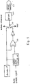
- the control signal Gf may be generated in response to a high voltage input to a test control circuit as shown in Figs. 7(a) or 7(b).
- the signal Gf is fixed at "H" level when the voltage of an address input is within the normal range, for example, a voltage range between 0 volt and 5 volt.
- the input voltage at the terminal 24 is out of the normal range, it is detected by the high voltage detection circuit 23.
- the signal Gf becomes "L” in response to the detection of the high voltage, for example, 9 volt.
- the mode is changed from the normal mode to the test mode. If the high voltage is not continuously applied to the input terminal 24, the test mode is not activated. Since one of the address input terminals is used in the embodiment of Fig. 7(a) for the high voltage input, not all addresses can be scanned during the test mode.
- FIG. 8(a) and 8(b) and Fig. 9 corresponds to the circuit (b).
- input address signals A6, A9, A14, A16 and output enable signal /OE are applied to high voltage detection circuits HVDT. These signals are also supplied to input buffer circuits of the memory circuit which are not shown in Fig. 9.
- An output signal of a high voltage detection circuit HVDT is "L" (logical L level) when the input signal is within a normal input voltage range, 0 volt to 5 volt.
- L logical L level
- NAND gates G6 and 68 In the normal mode, NAND gates G6 and 68 output "H".
- a latch enable signal LE is “L”, namely inactive.
- NOR gate G4 outputs “H” since nodes N1 to N3 are at “L” level.
- Reset signal RST is “L”, namely inactive.
- NAND gate G13 outputs "H” to node N4 regardless of the level of the input address (24) applied to flip-flop circuit FF. Therefore, signal Gf is fixed at "H” level during the normal mode.
- an input terminal /OE is used to receive the high voltage rather than A16.
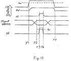
- the mode is changed from the normal mode to the test mode as follows. At time T1 shown in Fig. 10, the reset signal RST becomes "H” in response to the high voltage applied to one of input terminals /OE, A6 and A14.
- N4 still remains at "H", but the state of the flip-flop circuit FF is changeable in response to LE and the input address.
- the input address applied to the FF becomes valid.
- the latch enable signal LE becomes active “H” in response to the high voltage applied to the input terminal A9.
- the logic level of the input address is latched by the flip-flop FF. If the input address is "L” when LE rises, the signal Gf becomes “L”. If the input address is "H” when LE rises, the signal Gf remains “H”.
- the latch enable signal LE becomes "L” in response to release of the high voltage at the input terminal A9.
- the input terminals can be used for inputting addresses or other input signals during the test mode. It is not necessary to provide a special test control terminal according to the embodiment of Fig. 9.
- circuitry could be designed so that the defective bit lines are no longer selected, even in the write stress test (Y1 is not set to H in the example shown in Fig. 6).
- Y1 is not set to H in the example shown in Fig. 6
- the structure of the column gate selection circuit is complicated.
- the method of inserting the switch Qf to the common ground line is simple in structure and only requires that the signal Gf is set to L during the write stress test.
- an embodiment of the present invention can provide for performance of the write stress test even for an EPROM which uses bit line redundancy, and can avoid test failure due to problems with gate oxide film. Thereby, the present invention can provide for remarkable improvements in device reliability.
- An EPROM fails if memory cells mistakenly release accumulated charges. This can happen if the stored information in a cell is lost due to electrical stress suffered when information is written into adjacent cells.
- a so-called stress test is conducted to selectively isolate the cells which cannot withstand such stress. Since the write or read operation in an EPROM is sequentially conducted for individual cells, a longer time is taken for write or read operations but, such operations may be continued by replacing the defective cells with redundant cells.
- the stress test is preferably conducted by stressing all cells simultaneously, in order to improve efficiency.
- the present invention provides a capability for applying specified stress to all cells simultaneously, even if the power supply line is short-circuited to ground due to failure in one or more memory cells in the cell array. As a means for attaining this purpose, the common GND line and the short-circuit point are separated when a stress test voltage is applied.
Claims (14)
- Dispositif de mémoires non-volatiles à semi-conducteur, ayant un mode de fonctionnement normal et un mode de test, comprenant :une pluralité de lignes binaires (BLO, BL1, BLr) ;une pluralité de lignes de mots (X0, X1, Xi) qui coupent lesdites lignes binaires ;une pluralité de cellules de mémoires non-volatiles (Q00, Q10 à Q1i), ayant chacune un drain, une grille de commande et une source, les cellules étant reliées auxdites lignes binaires et auxdites lignes de mots où lesdites lignes binaires et lesdites lignes de mots se coupent, avec les drains reliés auxdites lignes binaires et les grilles de commande reliées auxdites lignes de mots ; etune ligne d'alimentation (GND) pour fournir au moins un potentiel prédéterminé aux sources de toutes lesdites cellules de mémoire ;caractérisé parun dispositif (Qf) pour isoler électriquement les sources desdites cellules de mémoire de ladite ligne d'alimentation en réponse à un signal de commande (Gf), ledit dispositif d'isolation comprenant un circuit de commutation (Qf) qui est conducteur pour fournir ledit potentiel prédéterminé aux sources desdites cellules de mémoire généralement pendant le mode de fonctionnement normal, ledit circuit de commutation étant bloqué pendant le mode de test pour isoler ladite ligne d'alimentation des sources desdites cellules de mémoire.
- Dispositif de mémoires non-volatiles à semi-conducteur selon la revendication 1, dans lequel lesdites cellules de mémoire sont normalement utilisées dans un intervalle de tension normale, ledit dispositif comprenant en outre :une pluralité de bornes d'entrée (24 ; A1 à A16 /OE,
 un circuit de commande de mode de test, relié à une telle borne d'entrée et audit circuit de commutation (Qf), pour générer ledit signal de commande (Gf), ledit circuit de commande de mode de test bloquant ledit circuit de commutation (Qf) en réponse à une tension de niveau haut qui dépasse l'intervalle de tension normal, ladite tension de niveau haut étant appliquée à ladite borne d'entrée.
 - Dispositif de mémoires non-volatiles à semi-conducteur selon la revendication 1, dans lequel lesdits cellules de mémoire sont normalement actionnées dans un intervalle de tension normal, ledit dispositif comprenant en outre :des première (A16, A6, A14, /OE), seconde (A9) et troisième (24) bornes d'entrée pour recevoir des signaux externes ; etun circuit de commande de mode de test, relié auxdites première, seconde et troisième bornes d'entrée et au circuit de commutation (Qf), pour générer ledit signal de commande, ledit circuit de commande de test comprenant :un circuit de bascule (FF) ayant une borne de réinitialisation (RST), une borne de validation de verrouillage (LE), une borne d'entrée et une borne de sortie,un premier circuit de détection de tension de niveau haut (30) pour fournir un signal de réinitialisation (RST) à ladite borne de réinitialisation lorsqu'une tension de niveau haut en dehors de l'intervalle de fonctionnement normal est appliquée à ladite première borne (A16, A6, A14 / OE), etun second circuit de détection de tension de niveau haut (31) pour fournir un signal de validation de verrouillage (LE) à ladite borne de validation de verrouillage lorsque ladite tension de niveau haut est appliquée à ladite seconde borne (A9),dans lequel un signal d'entrée appliqué à ladite troisième borne (24) est verrouillé dans ledit circuit de bascule (FF) en réponse audit signal de validation de verrouillage (LE).
- Dispositif de mémoires non-volatiles à semi-conducteur selon la revendication 3, dans lequel lesdites première, seconde et troisième bornes d'entrée sont des bornes d'entrée d'adresse.
- Dispositif de mémoires non-volatiles à semi-conducteur selon l'une quelconque des revendications précédentes, dans lequel ledit potentiel prédéterminé est un potentiel de masse (GND).
- Dispositif de mémoires non-volatiles à semi-conducteur selon l'une quelconque des revendications précédentes, dans lequel lesdites cellules de mémoire non-volatiles (Q00, Q10 à Q1i) comprennent des transistors FAMOS.
- Dispositif de mémoires non-volatiles à semi-conducteur selon l'une quelconque des revendications précédentes, ledit dispositif comprenant en outre un réseau de cellules de mémoire redondantes ayant une ligne binaire redondante (BLr) reliée audit circuit de commutation (Qf), ladite ligne binaire redondante étant isolée de ladite ligne d'alimentation (GND) par ledit circuit de commutation pendant le mode de test.
- Dispositif de mémoires non-volatiles à semi-conducteur selon l'une quelconque des revendications précédentes, ledit dispositif comprenant en outre un dispositif pour fournir une tension de programmation auxdites lignes binaires (BL0, BL1, BLr) pendant le mode de test et pour fournir un potentiel de masse auxdites lignes de mots.
- Dispositif de mémoires non-volatiles à semi-conducteur selon l'une quelconque des revendications précédentes, étant une mémoire programmable effaçable, dans lequelcertaines desdites lignes binaires (BLr) sont utilisées comme des lignes binaires redondantes,le dispositif comprend en outre un circuit d'écriture pour stocker de façon permanente des informations dans lesdites cellules de mémoire sélectionnées, lesdites lignes binaires étant aussi reliées audit circuit d'écriture, etledit dispositif (Qf) pour isoler électriquement lesdites sources desdites lignes d'alimentation (GND) sont utilisées dans le but de conduire un test de contrainte de façon simultanée sur toutes lesdites cellules de mémoire.
- Mémoire selon la revendication 9, dans laquelle toutes lesdites sources sont reliées à une liaison de masse à travers une ligne de masse commune unique, ledit dispositif d'isolation comprenant un commutateur unique (Qf) disposé entre ladite connexion de masse et ladite ligne de masse, ledit commutateur étant conducteur pendant un fonctionnement normal, et bloqué pendant ledit test de contrainte.
- Mémoire selon la revendication 10, dans laquelle ledit dispositif d'isolation comprend en outre un dispositif pour générer un signal de commande pendant ladite commutation en réponse à un signal d'adresse d'entrée sélectionné.
- Mémoire selon la revendication 11, dans laquelle ledit signal de commande est généré seulement lorsque ledit signal d'adresse est présent.
- Mémoire selon la revendication 11, dans laquelle ledit signal de commande est verrouillé de façon conducteur en réponse audit signal d'adresse, et reste jusqu'à ce que ledit signal de commande soit réinitialisé, indépendamment de si ledit signal d'adresse est présent de façon continue.
- Procédé pour tester un dispositif de mémoires non-volatiles à semi-conducteur ayant une pluralité de lignes binaires (BL0, BL1, BLr), une pluralité de lignes de mots (X0, X1, Xi) qui coupent les lignes binaires, et une pluralité de transistors de cellules de mémoire non-volatiles (Q00, Q10 à Q1i), ayant chacune un drain, une grille de commande et une source, reliés aux lignes binaires et aux lignes de mots où les lignes binaires et les lignes de mots se coupent, avec les drains reliés auxdites lignes binaires et les grilles de commande reliées auxdites lignes de mots, les sources ayant une liaison à une ligne de masse (GND) caractérisé par les étapes de :isolation électriquement des sources de la ligne de masse (GND) ; etapplication d'une contrainte électrique au transistor de cellules de mémoire en appliquant un potentiel de programmation aux lignes binaires et un potentiel de masse aux lignes de mots.
Applications Claiming Priority (2)
| Application Number | Priority Date | Filing Date | Title |
|---|---|---|---|
| JP29070489A JP3384409B2 (ja) | 1989-11-08 | 1989-11-08 | 書換え可能な不揮発性半導体記憶装置及びその制御方法 |
| JP290704/89 | 1989-11-08 |
Publications (3)
| Publication Number | Publication Date |
|---|---|
| EP0427260A2 EP0427260A2 (fr) | 1991-05-15 |
| EP0427260A3 EP0427260A3 (en) | 1992-04-22 |
| EP0427260B1 true EP0427260B1 (fr) | 1996-01-31 |
Family
ID=17759434
Family Applications (1)
| Application Number | Title | Priority Date | Filing Date |
|---|---|---|---|
| EP90121404A Expired - Lifetime EP0427260B1 (fr) | 1989-11-08 | 1990-11-08 | Dispositif de mémoires non-volatiles |
Country Status (4)
| Country | Link |
|---|---|
| EP (1) | EP0427260B1 (fr) |
| JP (1) | JP3384409B2 (fr) |
| KR (1) | KR950000342B1 (fr) |
| DE (1) | DE69025127T2 (fr) |
Families Citing this family (4)
| Publication number | Priority date | Publication date | Assignee | Title |
|---|---|---|---|---|
| KR960001307B1 (ko) * | 1990-10-02 | 1996-01-25 | 가부시기가이샤 도오시바 | 메모리의 테스트방법 |
| DE4133490C2 (de) * | 1991-10-09 | 1999-06-10 | Texas Instruments Deutschland | Verfahren zum Betreiben einer mit einer Versorgungsspannung gespeisten integrierten Halbleiterspeichervorrichtung mit zeilen- und spaltenweise angeordneten Speicherzellen |
| KR950003014B1 (ko) * | 1992-07-31 | 1995-03-29 | 삼성전자 주식회사 | 반도체 메모리 장치의 번-인 테스트회로 및 번-인 테스트방법 |
| KR20210121456A (ko) * | 2020-03-30 | 2021-10-08 | 에스케이하이닉스 주식회사 | 반도체 메모리 장치 및 이의 동작 방법 |
Family Cites Families (6)
| Publication number | Priority date | Publication date | Assignee | Title |
|---|---|---|---|---|
| JPS60103587A (ja) * | 1983-11-09 | 1985-06-07 | Toshiba Corp | 半導体記憶装置のメモリセルキヤパシタ電圧印加回路 |
| NL8400326A (nl) * | 1984-02-03 | 1985-09-02 | Philips Nv | Geintegreerde schakeling met veldeffecttransistoren en een programmeerbaar leesgeheugen. |
| JPS62177799A (ja) * | 1986-01-30 | 1987-08-04 | Toshiba Corp | 半導体記憶装置 |
| JPS62275399A (ja) * | 1986-05-23 | 1987-11-30 | Hitachi Ltd | 半導体集積回路装置 |
| US4967394A (en) * | 1987-09-09 | 1990-10-30 | Kabushiki Kaisha Toshiba | Semiconductor memory device having a test cell array |
| JPH01113999A (ja) * | 1987-10-28 | 1989-05-02 | Toshiba Corp | 不揮発性メモリのストレステスト回路 |
-
1989
- 1989-11-08 JP JP29070489A patent/JP3384409B2/ja not_active Expired - Lifetime
-
1990
- 1990-11-05 KR KR1019900017818A patent/KR950000342B1/ko not_active IP Right Cessation
- 1990-11-08 EP EP90121404A patent/EP0427260B1/fr not_active Expired - Lifetime
- 1990-11-08 DE DE69025127T patent/DE69025127T2/de not_active Expired - Fee Related
Also Published As
| Publication number | Publication date |
|---|---|
| EP0427260A2 (fr) | 1991-05-15 |
| DE69025127T2 (de) | 1996-06-05 |
| EP0427260A3 (en) | 1992-04-22 |
| JP3384409B2 (ja) | 2003-03-10 |
| KR910010532A (ko) | 1991-06-29 |
| KR950000342B1 (ko) | 1995-01-13 |
| JPH03152800A (ja) | 1991-06-28 |
| DE69025127D1 (de) | 1996-03-14 |
Similar Documents
| Publication | Publication Date | Title |
|---|---|---|
| US6266792B1 (en) | Semiconductor memory, memory device, and memory card | |
| US4514830A (en) | Defect-remediable semiconductor integrated circuit memory and spare substitution method in the same | |
| EP0293339B1 (fr) | Dispositif de mémoire permanente supportant un grand nombre de cycles de programmation | |
| US5140554A (en) | Integrated circuit fuse-link tester and test method | |
| US4672240A (en) | Programmable redundancy circuit | |
| US5485424A (en) | Semiconductor memory and redundant-address writing method | |
| US5287310A (en) | Memory with I/O mappable redundant columns | |
| US6496413B2 (en) | Semiconductor memory device for effecting erasing operation in block unit | |
| EP0930569A2 (fr) | Circuit d'ajustage de bit pour une mémoire flash | |
| US5847995A (en) | Nonvolatile semiconductor memory device having a plurality of blocks provided on a plurality of electrically isolated wells | |
| US4975881A (en) | Semiconductor memory device provided with an improved redundant decoder | |
| US4744058A (en) | Semiconductor programmable memory device and method of writing a predetermined pattern to same | |
| US4794568A (en) | Redundancy circuit for use in a semiconductor memory device | |
| EP0503100B1 (fr) | Memoire a semi-conducteur | |
| EP0881571B1 (fr) | Dispositif de mémoire à semiconducteur avec rédondance | |
| US5434814A (en) | Circuit for repairing defective read only memories with redundant NAND string | |
| US4870618A (en) | Semiconductor memory equipped with test circuit for testing data holding characteristic during data programming period | |
| US5400344A (en) | Semiconductor device with function of testing insulation defect between bit lines and testing method therefor | |
| EP0740308B1 (fr) | Dispositif de mémoire dynamique à semi-conducteur | |
| JP3848022B2 (ja) | 電気フューズ素子を備えた半導体集積回路装置 | |
| EP0427260B1 (fr) | Dispositif de mémoires non-volatiles | |
| US4464736A (en) | In-package E2 PROM redundancy | |
| US6812532B2 (en) | Semiconductor device with address programming circuit | |
| JPH09128991A (ja) | 冗長救済回路 | |
| US6545920B2 (en) | Defective address storage scheme for memory device |
Legal Events
| Date | Code | Title | Description |
|---|---|---|---|
| PUAI | Public reference made under article 153(3) epc to a published international application that has entered the european phase |
Free format text: ORIGINAL CODE: 0009012 |
|
| AK | Designated contracting states |
Kind code of ref document: A2 Designated state(s): DE FR GB |
|
| PUAL | Search report despatched |
Free format text: ORIGINAL CODE: 0009013 |
|
| AK | Designated contracting states |
Kind code of ref document: A3 Designated state(s): DE FR GB |
|
| 17P | Request for examination filed |
Effective date: 19921016 |
|
| 17Q | First examination report despatched |
Effective date: 19940622 |
|
| GRAA | (expected) grant |
Free format text: ORIGINAL CODE: 0009210 |
|
| AK | Designated contracting states |
Kind code of ref document: B1 Designated state(s): DE FR GB |
|
| REF | Corresponds to: |
Ref document number: 69025127 Country of ref document: DE Date of ref document: 19960314 |
|
| ET | Fr: translation filed | ||
| PLBE | No opposition filed within time limit |
Free format text: ORIGINAL CODE: 0009261 |
|
| STAA | Information on the status of an ep patent application or granted ep patent |
Free format text: STATUS: NO OPPOSITION FILED WITHIN TIME LIMIT |
|
| 26N | No opposition filed | ||
| REG | Reference to a national code |
Ref country code: GB Ref legal event code: IF02 |
|
| PGFP | Annual fee paid to national office [announced via postgrant information from national office to epo] |
Ref country code: GB Payment date: 20051102 Year of fee payment: 16 |
|
| PGFP | Annual fee paid to national office [announced via postgrant information from national office to epo] |
Ref country code: DE Payment date: 20051103 Year of fee payment: 16 |
|
| PGFP | Annual fee paid to national office [announced via postgrant information from national office to epo] |
Ref country code: FR Payment date: 20051108 Year of fee payment: 16 |
|
| PG25 | Lapsed in a contracting state [announced via postgrant information from national office to epo] |
Ref country code: DE Free format text: LAPSE BECAUSE OF NON-PAYMENT OF DUE FEES Effective date: 20070601 |
|
| GBPC | Gb: european patent ceased through non-payment of renewal fee |
Effective date: 20061108 |
|
| REG | Reference to a national code |
Ref country code: FR Ref legal event code: ST Effective date: 20070731 |
|
| PG25 | Lapsed in a contracting state [announced via postgrant information from national office to epo] |
Ref country code: GB Free format text: LAPSE BECAUSE OF NON-PAYMENT OF DUE FEES Effective date: 20061108 |
|
| PG25 | Lapsed in a contracting state [announced via postgrant information from national office to epo] |
Ref country code: FR Free format text: LAPSE BECAUSE OF NON-PAYMENT OF DUE FEES Effective date: 20061130 |