EP0425024B1 - Circuit pour limiter la tension de sortie d'un dispositif semi-conducteur monolithique de puissance attaquant une charge résonante connectée à l'alimentation - Google Patents
Circuit pour limiter la tension de sortie d'un dispositif semi-conducteur monolithique de puissance attaquant une charge résonante connectée à l'alimentation Download PDFInfo
- Publication number
- EP0425024B1 EP0425024B1 EP90202775A EP90202775A EP0425024B1 EP 0425024 B1 EP0425024 B1 EP 0425024B1 EP 90202775 A EP90202775 A EP 90202775A EP 90202775 A EP90202775 A EP 90202775A EP 0425024 B1 EP0425024 B1 EP 0425024B1
- Authority
- EP
- European Patent Office
- Prior art keywords
- transistor
- voltage
- terminal
- power device
- circuit
- Prior art date
- Legal status (The legal status is an assumption and is not a legal conclusion. Google has not performed a legal analysis and makes no representation as to the accuracy of the status listed.)
- Expired - Lifetime
Links
Images


Classifications
-
- H—ELECTRICITY
- H03—ELECTRONIC CIRCUITRY
- H03K—PULSE TECHNIQUE
- H03K17/00—Electronic switching or gating, i.e. not by contact-making and –breaking
- H03K17/51—Electronic switching or gating, i.e. not by contact-making and –breaking characterised by the components used
- H03K17/56—Electronic switching or gating, i.e. not by contact-making and –breaking characterised by the components used by the use, as active elements, of semiconductor devices
- H03K17/60—Electronic switching or gating, i.e. not by contact-making and –breaking characterised by the components used by the use, as active elements, of semiconductor devices the devices being bipolar transistors
- H03K17/615—Electronic switching or gating, i.e. not by contact-making and –breaking characterised by the components used by the use, as active elements, of semiconductor devices the devices being bipolar transistors in a Darlington configuration
-
- H—ELECTRICITY
- H03—ELECTRONIC CIRCUITRY
- H03K—PULSE TECHNIQUE
- H03K17/00—Electronic switching or gating, i.e. not by contact-making and –breaking
- H03K17/16—Modifications for eliminating interference voltages or currents
-
- H—ELECTRICITY
- H03—ELECTRONIC CIRCUITRY
- H03K—PULSE TECHNIQUE
- H03K17/00—Electronic switching or gating, i.e. not by contact-making and –breaking
- H03K17/16—Modifications for eliminating interference voltages or currents
- H03K17/161—Modifications for eliminating interference voltages or currents in field-effect transistor switches
- H03K17/162—Modifications for eliminating interference voltages or currents in field-effect transistor switches without feedback from the output circuit to the control circuit
Definitions
- the present invention relates to a circuit for limiting the output voltage of a monolithic semiconductor power device which drives a resonant load connected to a power supply.
- resonant loads such as an ignition coil or a transformer
- a semiconductor power device say, of the darlington type, which is periodically switched on and off by means of a control circuit operated by an appropriate input signal.
- the power device in substance operates like a switch that is opened or closed by the input signal provided by the control circuit.
- parasitic components are associated with the active components of the control circuit which, when the above voltage falls below ground, enter into conduction and shortcircuit the active components of the control circuit and jeopardize the operation of the same.
- US-A-4 471 237 discloses an output protection circuit as defined in the preamble of the independent claim.
- the object of the present invention is to a new circuit which prevents the output of the power device, that is, its collector connected to the load, from going to a negative voltage with respect to ground thus triggering the parasitic components.
- a load L in particular a transformer, connected to a node at a voltage Vb of a battery is driven by a power device, in particular a switch A, which is opened and closed by an input signal Vi provided by a control circuit C supplied with a voltage Vs. With Vc there is indicated the output voltage of the power device.
- control circuit C comprises, among other things, a transistor T4 in series with a resistor R.
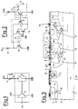
- the accomplishment in a monolithic integrated form of the circuit illustrated in Fig. 2 provides for a substrate with n+ doping, region 1, connected to the voltage Vc, inside which there are obtained transistors T5, T6 of the power darlington A, both of the npn type, whose collectors, bases, emitters occupy regions 2, 5, 6 and 2, 3, 4, respectively.
- the control device C of the power device A in particular the transistor T4 of the npn type, whose base, collector, emitter occupy regions 7, 8, 9 and whose collector, region 8, is connected to resistance R, region 10 of the p type, which in turn is connected to the power supply Vs.
- the monolithic accomplishment illustrated above determines the presence of a first parasitic transistor T1, whose base is accomplished in a region 11 of the pwell type, while the collector is accomplished in a region 12 of the n+ type and is connected to region 8 which constitutes the collector of transistor T4, and the emitter is accomplished in region 2 of the n- type.
- transistor T2 There are also present a second and a third parasitic transistor T2, T3.
- the base of transistor T2 is connected to the collector of transistor T3, obtained in a region 13 of the n+ type, the emitter is accomplished in the region 10 of the p type, the collector is connected to the base of transistor T3, region 11 of the pwell type, lastly the emitter of transistor T3 is accomplished inside region 2 of the n- type.
- the power device A accomplished by means of a pair of transistors T5, T6 in a darlington configuration, is driven on the base by control circuit C, kept on or off by means of input signal Vi.
- the emitter of the power device is grounded, the collector is connected to a load L, in particular a coil or a transformer.
- a voltage limiter in particular a zener Z1.
- Said limiting circuit L1 comprises a comparator B, which at its non-inverting input has a voltage Vrif, while its inverting input is supplied with the voltage Vc.
- a diode D1 is placed between the output U of comparator B and the voltage node Vc.
- limiting device L1 (Fig. 4) allows the avoidance of the negative voltage peaks Vc at instants tl and t2.
- comparator B is switched on when Vc is less than or equal to Vrif and supplies to the node at a voltage Vc the current necessary to avoid the undesired voltage peaks.
- a first circuit embodiment of the limiting circuit according to the invention.
- the node V1, which constitutes the input at the reference voltage of comparator B, is then connected to the base of a transistor T7, whose emitter is connected to a diode D2 and whose collector is connected to a resistor R3 in turn connected to the power supply Vs.
- An intermediate node V2, between the collector of transistor T7 and resistor R3, is connected to the base of a transistor T13, whose emitter is connected to the power supply Vs and whose collector is connected to the base of a transistor T9.
- the collector of transistor T9 is connected to the power supply Vs and the emitter to diode D1; in addition, between the base and the emitter of transistor T9 there is a resistor R6.
- V1 must be greater than Vbe and less than 2Vbe + Vsat(T5, T6) and thus the circuit according to the invention becomes consequently active when Vc is greater than -Vbe and less than Vsat(T5, T6).
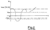
- Vc In the circuit of Fig. 6 the limitation of Vc thus occurs exclusively at two discrete values equal to Vbe and 0, while with the modification introduced in Fig. 7 Vc can be limited in a continuous manner, varying the values of R7 and R12, in an interval of values ranging from Vcesat(T5, T6) to - Vbe, excluding the extremes; this is shown in the graph of Fig. 8, where the thicker line refers to the preferred solution and the dotted lines indicate the upper and lower limits of such interval of values.
- the circuits according to the invention previously described may be accomplished with components of the MOS type or of the mixed type (bipolar + MOS) and they can be integrated in the structure shown in Fig. 9.
- the power darlington T5, T6 is replaced by a power MOS transistor, indicated in Fig. 9 with 30 whose gate is accomplished at polysilicon strips 43 while the source is accomplished in regions 42 of the type n 1 and the drain is accomplished in the substrate, region 2 of type n; the components of the control circuit are also of the MOS type, such as, say, M4, or they may be of the mixed type.
- the same reference numbers of Fig. 3 are used in Fig. 9 to indicate corresponding parts.
- FIG. 10 There is represented in Fig. 10 a circuit embodiment of the mixed type of the circuit illustrated in Fig. 6 with the variant of the voltage divider illustrated in Fig. 7.
- the bipolar transistors T13, T7 have been replaced here with MOS transistors M8, M7, an MOS transistor M31 has been introduced whose drain is connected to node V1, while the source is connected to the collector of transistor T11 and the gate is connected to the drain and thus to node V1; in addition, the power darlington T5, T6 has been replaced by the MOS power transistor M30.
Claims (6)
- Circuit limiteur de tension de sortie pour un dispositif de puissance à semiconducteur monolithique (T5, T6 ; M30) possédant une borne d'entrée recevant un signal d'entrée (Vi) et possédant une borne de sortie pour commander une charge résonnante (L), ledit circuit limiteur de tension de sortie comportant un comparateur (B) afin de comparer une tension de sortie (Vc) de ladite borne de sortie du dispositif de puissance (T5, T6 ; M30) à une tension de référence prédéterminée et pour délivrer un courant à la charge (L) lorsque ladite tension de sortie (Vc) devient plus faible que ladite tension de référence de manière à maintenir ladite tension de sortie (Vc) sensiblement égale à ladite tension de référence, et une première diode (D2) placée entre ladite borne de sortie et le comparateur (B) afin de protéger le comparateur (B) contre des surtensions de sortie du dispositif de puissance (T5, T6 ; M30), ledit comparateur (B) comportant un premier transistor (T7, M7) possédant une première borne reliée à une alimentation en tension (Vs), une seconde borne reliée à ladite borne de sortie du dispositif de puissance (T5, T6) par l'intermédiaire de ladite première diode (D2) et une borne de commande reliée à une source (G1, R2, D3-D5, R12, R7, T11, M31) de ladite tension de référence, caractérisé en ce que ledit comparateur (B) comporte en outre un second transistor (T9) possédant une première borne reliée à ladite alimentation en tension (Vs) et une seconde borne reliée à ladite borne de sortie du dispositif de puissance (T5, T6) par l'intermédiaire d'une seconde diode (D1), et un troisième transistor (T13, M8) possédant une première borne reliée à ladite alimentation en tension (Vs), une seconde borne reliée à une borne de commande du second transistor (T9) et une borne de commande reliée à la première borne du premier transistor (T7) afin de provoquer la mise en conduction du second transistor (T9) simultanément avec la mise en conduction du premier transistor (T7) tel que provoqué par un abaissement de la tension de sortie (Vc) du dispositif de puissance (T5, T6 ; M30) au-dessous de ladite tension de référence.
- circuit selon la revendication 1, caractérisé en ce que lesdits premier, second et troisième transistors (T7, T9, T13 ; M7, T9, M8) sont des transistors bipolaires (T7, T9, T13).
- circuit selon la revendication 2, caractérisé en ce que ladite source (G1, R2, D3-D5, R12, R7, T11, M31) de tension de référence consiste en un diviseur de tension (R2, D3-D5) possédant un noeud intermédiaire(V1) relié à la borne de commande dudit premier transistor (T7), ledit diviseur de tension (R2, D3-D5) comprenant une pluralité de diodes connectées en série (D3-D5) placées entre ledit noeud intermédiaire (V1) et la masse.
- Circuit selon la revendication 2, caractérisé en ce que ladite source (G1, R2, D3-D5, R12, R7, T11, M31) de tension de référence consiste en un diviseur de tension (G1, R2, R12, R7, T11) possédant un noeud intermédiaire (V1) relié à la borne de commande du premier transistor (T7), ledit diviseur de tension (G1, R2, R12, R7, T11) comprenant un transistor bipolaire (T11) placé entre ledit noeud intermédiaire (V1) et la masse et possédant une borne de commande reliée de façon résistive audit noeud intermédiaire (V1) et à la masse.
- Circuit selon la revendication 1, caractérisé en ce que lesdits premier et troisième transistors (T7, T13 ; M7, M8) sont des transistors MOS (M7, M8) et ledit second transistor (T9) est un transistor bipolaire.
- Circuit selon la revendication 5, caractérisé en ce que ladite source (G1, R2, D3-D5, R7, R12, T11, M31) de tension de référence consiste en un diviseur de tension (G1, R2, R7, R12, T11, M31) possédant un noeud intermédiaire (V1) relié à la borne de commande dudit premier transistor (M7), ledit diviseur de tension (G1, R2, R7, T11, M31) comprenant un montage série d'un transistor MOS additionnel (M31) et d'un transistor bipolaire (T11) possédant une borne de commande reliée de façon résistive audit transistor MOS additionnel (M31) et à la masse.
Applications Claiming Priority (2)
| Application Number | Priority Date | Filing Date | Title |
|---|---|---|---|
| IT2210489 | 1989-10-24 | ||
| IT02210489A IT1236627B (it) | 1989-10-24 | 1989-10-24 | Circuito di limitazione della tensione di uscita di un dispositivo monolitico di potenza a semiconduttore che pilota un carico risonante collegato ad un'alimentazione |
Publications (3)
| Publication Number | Publication Date |
|---|---|
| EP0425024A2 EP0425024A2 (fr) | 1991-05-02 |
| EP0425024A3 EP0425024A3 (en) | 1992-05-20 |
| EP0425024B1 true EP0425024B1 (fr) | 1998-08-12 |
Family
ID=11191556
Family Applications (1)
| Application Number | Title | Priority Date | Filing Date |
|---|---|---|---|
| EP90202775A Expired - Lifetime EP0425024B1 (fr) | 1989-10-24 | 1990-10-18 | Circuit pour limiter la tension de sortie d'un dispositif semi-conducteur monolithique de puissance attaquant une charge résonante connectée à l'alimentation |
Country Status (6)
| Country | Link |
|---|---|
| US (1) | US5189317A (fr) |
| EP (1) | EP0425024B1 (fr) |
| JP (1) | JP2745433B2 (fr) |
| KR (1) | KR100213582B1 (fr) |
| DE (1) | DE69032552T2 (fr) |
| IT (1) | IT1236627B (fr) |
Families Citing this family (5)
| Publication number | Priority date | Publication date | Assignee | Title |
|---|---|---|---|---|
| US5424663A (en) * | 1993-04-22 | 1995-06-13 | North American Philips Corporation | Integrated high voltage differential sensor using the inverse gain of high voltage transistors |
| EP0715409B1 (fr) * | 1994-11-30 | 1999-02-17 | STMicroelectronics S.r.l. | Circuit pour limiter la tension de sortie d'un transistor de puissance |
| EP0805554B1 (fr) * | 1996-04-30 | 2003-07-30 | STMicroelectronics S.r.l. | Circuit pour la recirculation contrôlée sans oscillation d'un courant de décharge d'une charge inductive |
| CN101770844B (zh) * | 2009-01-06 | 2012-01-11 | 安泰汽车电气系统(昆山)有限公司 | 电磁线圈驱动电路 |
| KR101307788B1 (ko) * | 2011-12-06 | 2013-09-12 | 주식회사 티엘아이 | 씨모스 출력 전압 제한 회로 |
Family Cites Families (6)
| Publication number | Priority date | Publication date | Assignee | Title |
|---|---|---|---|---|
| US4241309A (en) * | 1978-10-05 | 1980-12-23 | Andros Incorporated | Synchronizing method and apparatus |
| FR2467407A1 (fr) * | 1979-10-15 | 1981-04-17 | Jaeger | Dispositif de mesure des valeurs cretes d'un phenomene non periodique a recurrence faible |
| US4471237A (en) * | 1982-08-13 | 1984-09-11 | Rca Corporation | Output protection circuit for preventing a reverse current |
| DE3403327A1 (de) * | 1984-01-31 | 1985-08-01 | Siemens AG, 1000 Berlin und 8000 München | Schaltungsanordnung zur minimierung der wirkung parasitaerer transistorfunktionselemente in integrierten bipolaren halbleiterschaltkreisen |
| US4679112A (en) * | 1986-07-31 | 1987-07-07 | General Motors Corporation | Transistor protection circuit for automotive motor control applications |
| JP3032406U (ja) * | 1996-06-13 | 1996-12-24 | 有限会社日医商事 | マット・セット |
-
1989
- 1989-10-24 IT IT02210489A patent/IT1236627B/it active IP Right Grant
-
1990
- 1990-10-18 EP EP90202775A patent/EP0425024B1/fr not_active Expired - Lifetime
- 1990-10-18 DE DE69032552T patent/DE69032552T2/de not_active Expired - Fee Related
- 1990-10-22 US US07/600,870 patent/US5189317A/en not_active Expired - Lifetime
- 1990-10-24 JP JP2284550A patent/JP2745433B2/ja not_active Expired - Fee Related
- 1990-10-24 KR KR1019900017125A patent/KR100213582B1/ko not_active IP Right Cessation
Also Published As
| Publication number | Publication date |
|---|---|
| DE69032552D1 (de) | 1998-09-17 |
| EP0425024A3 (en) | 1992-05-20 |
| US5189317A (en) | 1993-02-23 |
| DE69032552T2 (de) | 1999-02-25 |
| IT8922104A1 (it) | 1991-04-24 |
| KR100213582B1 (ko) | 1999-08-02 |
| IT1236627B (it) | 1993-03-25 |
| IT8922104A0 (it) | 1989-10-24 |
| EP0425024A2 (fr) | 1991-05-02 |
| KR910008907A (ko) | 1991-05-31 |
| JP2745433B2 (ja) | 1998-04-28 |
| JPH03150612A (ja) | 1991-06-27 |
Similar Documents
| Publication | Publication Date | Title |
|---|---|---|
| US4360744A (en) | Semiconductor switching circuits | |
| US6236122B1 (en) | Load drive device | |
| EP0622717B1 (fr) | Circuit à récirculation de courant de décharge de charge inductive avec compensation en température | |
| US4345296A (en) | Device for controlling the current through an inductive consumer, especially a magnetic valve in the fuel metering system of an internal combustion engine | |
| US4970620A (en) | FET bridge protection circuit | |
| US4015143A (en) | Semiconductor switch | |
| US5473201A (en) | Control circuit means for controlling the after-running of an operating device in a motor vehicle | |
| US5010439A (en) | Control circuit for the clamping voltage of an inductive load driven by a power device in a high side driver configuration | |
| US4723191A (en) | Electronic voltage regulator for use in vehicles with protection against transient overvoltages | |
| CA1217529A (fr) | Circuit de declenchement pour commutateur a semiconducteur | |
| EP0425024B1 (fr) | Circuit pour limiter la tension de sortie d'un dispositif semi-conducteur monolithique de puissance attaquant une charge résonante connectée à l'alimentation | |
| US4564769A (en) | Saturation control of a switching transistor | |
| GB2140997A (en) | Circuit for preventing excessive power dissipation in power switching semiconductors | |
| US4882532A (en) | Active overvoltage control for inductive load driving | |
| US5111353A (en) | Overvoltage protection circuit | |
| US4916378A (en) | Inductive load discharge current recirculation circuit with selectable "fast" and "low" modes | |
| US4410809A (en) | Static induction transistor gate driving circuit | |
| EP0287525B1 (fr) | Recirculation du courant transitoire par un transistor de commutation de puissance commandant une charge inductive | |
| US5636097A (en) | Protective circuit for semiconductor power device | |
| CA1046142A (fr) | Circuit d'excitation pour commander la conduction d'un dispositif a semiconducteur | |
| GB2053606A (en) | Improvements in and relating to semiconductor switching circuits | |
| US5945868A (en) | Power semiconductor device and method for increasing turn-on time of the power semiconductor device | |
| US5495198A (en) | Snubbing clamp network | |
| US4639616A (en) | Circuit for controlling the base of a power transistor used in high tension switching | |
| US4096429A (en) | Voltage and current regulator for generating systems |
Legal Events
| Date | Code | Title | Description |
|---|---|---|---|
| PUAI | Public reference made under article 153(3) epc to a published international application that has entered the european phase |
Free format text: ORIGINAL CODE: 0009012 |
|
| AK | Designated contracting states |
Kind code of ref document: A2 Designated state(s): DE FR GB NL SE |
|
| PUAL | Search report despatched |
Free format text: ORIGINAL CODE: 0009013 |
|
| AK | Designated contracting states |
Kind code of ref document: A3 Designated state(s): DE FR GB NL SE |
|
| 17P | Request for examination filed |
Effective date: 19920921 |
|
| 17Q | First examination report despatched |
Effective date: 19950731 |
|
| GRAG | Despatch of communication of intention to grant |
Free format text: ORIGINAL CODE: EPIDOS AGRA |
|
| GRAG | Despatch of communication of intention to grant |
Free format text: ORIGINAL CODE: EPIDOS AGRA |
|
| GRAH | Despatch of communication of intention to grant a patent |
Free format text: ORIGINAL CODE: EPIDOS IGRA |
|
| GRAH | Despatch of communication of intention to grant a patent |
Free format text: ORIGINAL CODE: EPIDOS IGRA |
|
| GRAA | (expected) grant |
Free format text: ORIGINAL CODE: 0009210 |
|
| AK | Designated contracting states |
Kind code of ref document: B1 Designated state(s): DE FR GB NL SE |
|
| PG25 | Lapsed in a contracting state [announced via postgrant information from national office to epo] |
Ref country code: NL Free format text: LAPSE BECAUSE OF FAILURE TO SUBMIT A TRANSLATION OF THE DESCRIPTION OR TO PAY THE FEE WITHIN THE PRESCRIBED TIME-LIMIT Effective date: 19980812 |
|
| RAP4 | Party data changed (patent owner data changed or rights of a patent transferred) |
Owner name: STMICROELECTRONICS S.R.L. |
|
| REF | Corresponds to: |
Ref document number: 69032552 Country of ref document: DE Date of ref document: 19980917 |
|
| PG25 | Lapsed in a contracting state [announced via postgrant information from national office to epo] |
Ref country code: SE Free format text: LAPSE BECAUSE OF FAILURE TO SUBMIT A TRANSLATION OF THE DESCRIPTION OR TO PAY THE FEE WITHIN THE PRESCRIBED TIME-LIMIT Effective date: 19981112 |
|
| ET | Fr: translation filed | ||
| NLV1 | Nl: lapsed or annulled due to failure to fulfill the requirements of art. 29p and 29m of the patents act | ||
| PLBE | No opposition filed within time limit |
Free format text: ORIGINAL CODE: 0009261 |
|
| STAA | Information on the status of an ep patent application or granted ep patent |
Free format text: STATUS: NO OPPOSITION FILED WITHIN TIME LIMIT |
|
| 26N | No opposition filed | ||
| REG | Reference to a national code |
Ref country code: FR Ref legal event code: D6 |
|
| PGFP | Annual fee paid to national office [announced via postgrant information from national office to epo] |
Ref country code: GB Payment date: 20001018 Year of fee payment: 11 |
|
| PG25 | Lapsed in a contracting state [announced via postgrant information from national office to epo] |
Ref country code: GB Free format text: LAPSE BECAUSE OF NON-PAYMENT OF DUE FEES Effective date: 20011018 |
|
| REG | Reference to a national code |
Ref country code: GB Ref legal event code: IF02 |
|
| GBPC | Gb: european patent ceased through non-payment of renewal fee |
Effective date: 20011018 |
|
| PGFP | Annual fee paid to national office [announced via postgrant information from national office to epo] |
Ref country code: FR Payment date: 20021008 Year of fee payment: 13 |
|
| PGFP | Annual fee paid to national office [announced via postgrant information from national office to epo] |
Ref country code: DE Payment date: 20021024 Year of fee payment: 13 |
|
| PG25 | Lapsed in a contracting state [announced via postgrant information from national office to epo] |
Ref country code: DE Free format text: LAPSE BECAUSE OF NON-PAYMENT OF DUE FEES Effective date: 20040501 |
|
| PG25 | Lapsed in a contracting state [announced via postgrant information from national office to epo] |
Ref country code: FR Free format text: LAPSE BECAUSE OF NON-PAYMENT OF DUE FEES Effective date: 20040630 |
|
| REG | Reference to a national code |
Ref country code: FR Ref legal event code: ST |