EP0425024B1 - Circuit for limiting the output voltage of a monolithic semiconductor power device which drives a resonant load connected to a power supply - Google Patents
Circuit for limiting the output voltage of a monolithic semiconductor power device which drives a resonant load connected to a power supply Download PDFInfo
- Publication number
- EP0425024B1 EP0425024B1 EP90202775A EP90202775A EP0425024B1 EP 0425024 B1 EP0425024 B1 EP 0425024B1 EP 90202775 A EP90202775 A EP 90202775A EP 90202775 A EP90202775 A EP 90202775A EP 0425024 B1 EP0425024 B1 EP 0425024B1
- Authority
- EP
- European Patent Office
- Prior art keywords
- transistor
- voltage
- terminal
- power device
- circuit
- Prior art date
- Legal status (The legal status is an assumption and is not a legal conclusion. Google has not performed a legal analysis and makes no representation as to the accuracy of the status listed.)
- Expired - Lifetime
Links
Images


Classifications
-
- H—ELECTRICITY
- H03—ELECTRONIC CIRCUITRY
- H03K—PULSE TECHNIQUE
- H03K17/00—Electronic switching or gating, i.e. not by contact-making and –breaking
- H03K17/51—Electronic switching or gating, i.e. not by contact-making and –breaking characterised by the components used
- H03K17/56—Electronic switching or gating, i.e. not by contact-making and –breaking characterised by the components used by the use, as active elements, of semiconductor devices
- H03K17/60—Electronic switching or gating, i.e. not by contact-making and –breaking characterised by the components used by the use, as active elements, of semiconductor devices the devices being bipolar transistors
- H03K17/615—Electronic switching or gating, i.e. not by contact-making and –breaking characterised by the components used by the use, as active elements, of semiconductor devices the devices being bipolar transistors in a Darlington configuration
-
- H—ELECTRICITY
- H03—ELECTRONIC CIRCUITRY
- H03K—PULSE TECHNIQUE
- H03K17/00—Electronic switching or gating, i.e. not by contact-making and –breaking
- H03K17/16—Modifications for eliminating interference voltages or currents
-
- H—ELECTRICITY
- H03—ELECTRONIC CIRCUITRY
- H03K—PULSE TECHNIQUE
- H03K17/00—Electronic switching or gating, i.e. not by contact-making and –breaking
- H03K17/16—Modifications for eliminating interference voltages or currents
- H03K17/161—Modifications for eliminating interference voltages or currents in field-effect transistor switches
- H03K17/162—Modifications for eliminating interference voltages or currents in field-effect transistor switches without feedback from the output circuit to the control circuit
Landscapes
- Electronic Switches (AREA)
- Control Of Voltage And Current In General (AREA)
- Control Of Electrical Variables (AREA)
- Continuous-Control Power Sources That Use Transistors (AREA)
- Amplifiers (AREA)
- Bipolar Integrated Circuits (AREA)
- Dc-Dc Converters (AREA)
- Emergency Protection Circuit Devices (AREA)
Description
Claims (6)
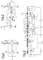
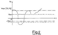
- Output voltage limiting circuit for a monolithic semiconductor power device (T5, T6; M30) having an input terminal receiving an input signal (Vi) and having an output terminal for controlling a resonant load (L), said output voltage limiting circuit comprising a comparator (B) for comparing an output voltage (Vc) at said output terminal of the power device (T5, T6; M30) with a predetermined reference voltage and for supplying current to the load (L) when said output voltage (Vc) becomes lower than said reference voltage so as to maintain said output voltage (Vc) substantially equal to said reference voltage, and first diode means (D2) interposed between said output terminal and the comparator (B) to protect the comparator (B) against output overvoltages of the power device (T5, T6; M30), said comparator (B) comprising a first transistor (T7, M7) having a first terminal connected to a voltage supply (Vs), a second terminal connected to said output terminal of the power device (T5, T6) through said first diode means (D2) and a control terminal connected to a source (G1, R2, D3-D5, R12, R7, T11, M31) of said reference voltage, characterized in that said comparator (B) further comprises second transistor (T9) having a first terminal connected to said voltage supply (Vs) and a second terminal connected to said output terminal of the power device (T5, T6) through second diode means (D1), and a third transistor (T13, M8) having a first terminal connected to said voltage supply (Vs), a second terminal connected to a control terminal of the second transistor (T9) and a control terminal connected to the first terminal of the first transistor (T7) to cause switching on of the second transistor (T9) simultaneously with switching on of the first transistor (T7) as caused by lowering of the output voltage (Vc) of the power device (T5, T6; M30) under said reference voltage.
- Circuit according to claim 1, characterized in that said first, second and third transistors (T7, T9, T13; M7, T9, M8) are bipolar transistors (T7, T9, T13).
- Circuit according to claim 2, characterized in that said source (G1, R2, D3-D5, R12, R7, T11, M31) of reference voltage consists of a voltage divider (R2, D3-D5) having an intermediate node (V1) connected to the control terminal of said first transistor (T7), said voltage divider (R2, D3-D5) including a plurality of serially connected diodes (D3-D5) interposed between said intermediate node (V1) and ground.
- Circuit according to claim 2, characterized in that said source (G1, R2, D3-D5, R12, R7, T11, M31) of reference voltage consists of a voltage divider (G1, R2, R12, R7, T11) having an intermediate node (V1) connected to the control terminal of said first transistor (T7), said voltage divider (G1, R2, R12, R7, T11) including a bipolar transistor (T11) interposed between said intermediate node (V1) and ground and having a control terminal resistively connected to said intermediate node (V1) and ground.
- Circuit according to claim 1, characterized in that said first and third transistors (T7, T13; M7, M8) are MOS transistors (M7, M8) and said second transistor (T9) is a bipolar transistor.
- Circuit according to claim 5, characterized in that said source (G1, R2, D3-D5, R7, R12, T11, M31) of reference voltage consists of a voltage divider (G1, R2, R7, R12, T11, M31) having an intermediate node (V1) connected to the control terminal of said first transistor (M7), said voltage divider (G1, R2, R7, R12, T11, M31) including a series of an additional MOS transistor (M31) and of a bipolar transistor (T11) having a control terminal resistively connected to said additional MOS transistor (M31) and ground.
Applications Claiming Priority (2)
| Application Number | Priority Date | Filing Date | Title |
|---|---|---|---|
| IT02210489A IT1236627B (en) | 1989-10-24 | 1989-10-24 | CIRCUIT FOR LIMITING THE OUTPUT VOLTAGE OF A MONOLITHIC POWER DEVICE WITH A SEMICONDUCTOR THAT DRIVES A RESONANT LOAD CONNECTED TO A POWER SUPPLY |
| IT2210489 | 1989-10-24 |
Publications (3)
| Publication Number | Publication Date |
|---|---|
| EP0425024A2 EP0425024A2 (en) | 1991-05-02 |
| EP0425024A3 EP0425024A3 (en) | 1992-05-20 |
| EP0425024B1 true EP0425024B1 (en) | 1998-08-12 |
Family
ID=11191556
Family Applications (1)
| Application Number | Title | Priority Date | Filing Date |
|---|---|---|---|
| EP90202775A Expired - Lifetime EP0425024B1 (en) | 1989-10-24 | 1990-10-18 | Circuit for limiting the output voltage of a monolithic semiconductor power device which drives a resonant load connected to a power supply |
Country Status (6)
| Country | Link |
|---|---|
| US (1) | US5189317A (en) |
| EP (1) | EP0425024B1 (en) |
| JP (1) | JP2745433B2 (en) |
| KR (1) | KR100213582B1 (en) |
| DE (1) | DE69032552T2 (en) |
| IT (1) | IT1236627B (en) |
Families Citing this family (5)
| Publication number | Priority date | Publication date | Assignee | Title |
|---|---|---|---|---|
| US5424663A (en) * | 1993-04-22 | 1995-06-13 | North American Philips Corporation | Integrated high voltage differential sensor using the inverse gain of high voltage transistors |
| DE69416595T2 (en) * | 1994-11-30 | 1999-06-17 | St Microelectronics Srl | Circuit for limiting the output voltage of a power transistor |
| EP0805554B1 (en) * | 1996-04-30 | 2003-07-30 | STMicroelectronics S.r.l. | Circuit for the controlled recycle without oscillation of a discharge current from an inductive load |
| CN101770844B (en) * | 2009-01-06 | 2012-01-11 | 安泰汽车电气系统(昆山)有限公司 | Electromagnetic coil driving circuit |
| KR101307788B1 (en) * | 2011-12-06 | 2013-09-12 | 주식회사 티엘아이 | Cmos output voltage limiter |
Family Cites Families (6)
| Publication number | Priority date | Publication date | Assignee | Title |
|---|---|---|---|---|
| US4241309A (en) * | 1978-10-05 | 1980-12-23 | Andros Incorporated | Synchronizing method and apparatus |
| FR2467407A1 (en) * | 1979-10-15 | 1981-04-17 | Jaeger | DEVICE FOR MEASURING VALUES CREATED FROM A NON-PERIODIC PHENOMENON WITH LOW RECURRENCE |
| US4471237A (en) * | 1982-08-13 | 1984-09-11 | Rca Corporation | Output protection circuit for preventing a reverse current |
| DE3403327A1 (en) * | 1984-01-31 | 1985-08-01 | Siemens AG, 1000 Berlin und 8000 München | CIRCUIT ARRANGEMENT FOR MINIMIZING THE EFFECT OF PARASITAL TRANSISTOR FUNCTION ELEMENTS IN INTEGRATED BIPOLAR SEMICONDUCTOR CIRCUITS |
| US4679112A (en) * | 1986-07-31 | 1987-07-07 | General Motors Corporation | Transistor protection circuit for automotive motor control applications |
| JP3032406U (en) * | 1996-06-13 | 1996-12-24 | 有限会社日医商事 | Matte set |
-
1989
- 1989-10-24 IT IT02210489A patent/IT1236627B/en active IP Right Grant
-
1990
- 1990-10-18 DE DE69032552T patent/DE69032552T2/en not_active Expired - Fee Related
- 1990-10-18 EP EP90202775A patent/EP0425024B1/en not_active Expired - Lifetime
- 1990-10-22 US US07/600,870 patent/US5189317A/en not_active Expired - Lifetime
- 1990-10-24 KR KR1019900017125A patent/KR100213582B1/en not_active IP Right Cessation
- 1990-10-24 JP JP2284550A patent/JP2745433B2/en not_active Expired - Fee Related
Also Published As
| Publication number | Publication date |
|---|---|
| EP0425024A3 (en) | 1992-05-20 |
| IT8922104A1 (en) | 1991-04-24 |
| KR100213582B1 (en) | 1999-08-02 |
| DE69032552T2 (en) | 1999-02-25 |
| US5189317A (en) | 1993-02-23 |
| IT1236627B (en) | 1993-03-25 |
| IT8922104A0 (en) | 1989-10-24 |
| DE69032552D1 (en) | 1998-09-17 |
| JPH03150612A (en) | 1991-06-27 |
| JP2745433B2 (en) | 1998-04-28 |
| EP0425024A2 (en) | 1991-05-02 |
| KR910008907A (en) | 1991-05-31 |
Similar Documents
| Publication | Publication Date | Title |
|---|---|---|
| US4360744A (en) | Semiconductor switching circuits | |
| US6236122B1 (en) | Load drive device | |
| EP0622717B1 (en) | Temperature stable circuit for recycling discharge current during the driving of an inductive load | |
| US4345296A (en) | Device for controlling the current through an inductive consumer, especially a magnetic valve in the fuel metering system of an internal combustion engine | |
| US6396249B1 (en) | Load actuation circuit | |
| US4970620A (en) | FET bridge protection circuit | |
| US5473201A (en) | Control circuit means for controlling the after-running of an operating device in a motor vehicle | |
| US5010439A (en) | Control circuit for the clamping voltage of an inductive load driven by a power device in a high side driver configuration | |
| US4723191A (en) | Electronic voltage regulator for use in vehicles with protection against transient overvoltages | |
| CA1217529A (en) | Trigger circuit for solid state switch | |
| EP0425024B1 (en) | Circuit for limiting the output voltage of a monolithic semiconductor power device which drives a resonant load connected to a power supply | |
| US4564769A (en) | Saturation control of a switching transistor | |
| GB2140997A (en) | Circuit for preventing excessive power dissipation in power switching semiconductors | |
| US4882532A (en) | Active overvoltage control for inductive load driving | |
| US5111353A (en) | Overvoltage protection circuit | |
| US4916378A (en) | Inductive load discharge current recirculation circuit with selectable "fast" and "low" modes | |
| US4410809A (en) | Static induction transistor gate driving circuit | |
| EP0287525B1 (en) | Transitory current recirculation through a power switching transistor driving an inductive load | |
| US5636097A (en) | Protective circuit for semiconductor power device | |
| CA1046142A (en) | Drive circuit for controlling conduction of a semiconductor device | |
| US5495198A (en) | Snubbing clamp network | |
| GB2053606A (en) | Improvements in and relating to semiconductor switching circuits | |
| US5945868A (en) | Power semiconductor device and method for increasing turn-on time of the power semiconductor device | |
| US4639616A (en) | Circuit for controlling the base of a power transistor used in high tension switching | |
| US4096429A (en) | Voltage and current regulator for generating systems |
Legal Events
| Date | Code | Title | Description |
|---|---|---|---|
| PUAI | Public reference made under article 153(3) epc to a published international application that has entered the european phase |
Free format text: ORIGINAL CODE: 0009012 |
|
| AK | Designated contracting states |
Kind code of ref document: A2 Designated state(s): DE FR GB NL SE |
|
| PUAL | Search report despatched |
Free format text: ORIGINAL CODE: 0009013 |
|
| AK | Designated contracting states |
Kind code of ref document: A3 Designated state(s): DE FR GB NL SE |
|
| 17P | Request for examination filed |
Effective date: 19920921 |
|
| 17Q | First examination report despatched |
Effective date: 19950731 |
|
| GRAG | Despatch of communication of intention to grant |
Free format text: ORIGINAL CODE: EPIDOS AGRA |
|
| GRAG | Despatch of communication of intention to grant |
Free format text: ORIGINAL CODE: EPIDOS AGRA |
|
| GRAH | Despatch of communication of intention to grant a patent |
Free format text: ORIGINAL CODE: EPIDOS IGRA |
|
| GRAH | Despatch of communication of intention to grant a patent |
Free format text: ORIGINAL CODE: EPIDOS IGRA |
|
| GRAA | (expected) grant |
Free format text: ORIGINAL CODE: 0009210 |
|
| AK | Designated contracting states |
Kind code of ref document: B1 Designated state(s): DE FR GB NL SE |
|
| PG25 | Lapsed in a contracting state [announced via postgrant information from national office to epo] |
Ref country code: NL Free format text: LAPSE BECAUSE OF FAILURE TO SUBMIT A TRANSLATION OF THE DESCRIPTION OR TO PAY THE FEE WITHIN THE PRESCRIBED TIME-LIMIT Effective date: 19980812 |
|
| RAP4 | Party data changed (patent owner data changed or rights of a patent transferred) |
Owner name: STMICROELECTRONICS S.R.L. |
|
| REF | Corresponds to: |
Ref document number: 69032552 Country of ref document: DE Date of ref document: 19980917 |
|
| PG25 | Lapsed in a contracting state [announced via postgrant information from national office to epo] |
Ref country code: SE Free format text: LAPSE BECAUSE OF FAILURE TO SUBMIT A TRANSLATION OF THE DESCRIPTION OR TO PAY THE FEE WITHIN THE PRESCRIBED TIME-LIMIT Effective date: 19981112 |
|
| ET | Fr: translation filed | ||
| NLV1 | Nl: lapsed or annulled due to failure to fulfill the requirements of art. 29p and 29m of the patents act | ||
| PLBE | No opposition filed within time limit |
Free format text: ORIGINAL CODE: 0009261 |
|
| STAA | Information on the status of an ep patent application or granted ep patent |
Free format text: STATUS: NO OPPOSITION FILED WITHIN TIME LIMIT |
|
| 26N | No opposition filed | ||
| REG | Reference to a national code |
Ref country code: FR Ref legal event code: D6 |
|
| PGFP | Annual fee paid to national office [announced via postgrant information from national office to epo] |
Ref country code: GB Payment date: 20001018 Year of fee payment: 11 |
|
| PG25 | Lapsed in a contracting state [announced via postgrant information from national office to epo] |
Ref country code: GB Free format text: LAPSE BECAUSE OF NON-PAYMENT OF DUE FEES Effective date: 20011018 |
|
| REG | Reference to a national code |
Ref country code: GB Ref legal event code: IF02 |
|
| GBPC | Gb: european patent ceased through non-payment of renewal fee |
Effective date: 20011018 |
|
| PGFP | Annual fee paid to national office [announced via postgrant information from national office to epo] |
Ref country code: FR Payment date: 20021008 Year of fee payment: 13 |
|
| PGFP | Annual fee paid to national office [announced via postgrant information from national office to epo] |
Ref country code: DE Payment date: 20021024 Year of fee payment: 13 |
|
| PG25 | Lapsed in a contracting state [announced via postgrant information from national office to epo] |
Ref country code: DE Free format text: LAPSE BECAUSE OF NON-PAYMENT OF DUE FEES Effective date: 20040501 |
|
| PG25 | Lapsed in a contracting state [announced via postgrant information from national office to epo] |
Ref country code: FR Free format text: LAPSE BECAUSE OF NON-PAYMENT OF DUE FEES Effective date: 20040630 |
|
| REG | Reference to a national code |
Ref country code: FR Ref legal event code: ST |