EP0422656B1 - Informationsverarbeitungsanordnung - Google Patents
Informationsverarbeitungsanordnung Download PDFInfo
- Publication number
- EP0422656B1 EP0422656B1 EP90119527A EP90119527A EP0422656B1 EP 0422656 B1 EP0422656 B1 EP 0422656B1 EP 90119527 A EP90119527 A EP 90119527A EP 90119527 A EP90119527 A EP 90119527A EP 0422656 B1 EP0422656 B1 EP 0422656B1
- Authority
- EP
- European Patent Office
- Prior art keywords
- request
- memory
- data buffer
- cache
- cache invalidation
- Prior art date
- Legal status (The legal status is an assumption and is not a legal conclusion. Google has not performed a legal analysis and makes no representation as to the accuracy of the status listed.)
- Expired - Lifetime
Links
Images
Classifications
-
- G—PHYSICS
- G06—COMPUTING OR CALCULATING; COUNTING
- G06F—ELECTRIC DIGITAL DATA PROCESSING
- G06F12/00—Accessing, addressing or allocating within memory systems or architectures
- G06F12/02—Addressing or allocation; Relocation
- G06F12/08—Addressing or allocation; Relocation in hierarchically structured memory systems, e.g. virtual memory systems
- G06F12/0802—Addressing of a memory level in which the access to the desired data or data block requires associative addressing means, e.g. caches
- G06F12/0806—Multiuser, multiprocessor or multiprocessing cache systems
- G06F12/0815—Cache consistency protocols
- G06F12/0817—Cache consistency protocols using directory methods
Definitions
- the present invention relates to an information processing system and, more particularly, to a cache invalidation control system.
- a memory access control unit comprises a first control unit which operates in synchronism with the request source, and a second control unit which operates in synchronism with the main memory.
- the first control unit accepts the request and stores memory access information in a data buffer predetermined for each request source.
- the information is stored in the data buffer until it is read out by a read address stored in the first control unit in order to send a processor number which is a part of the memory access information stored in the data buffer or reply information indicating the presence/absence of reply data to an arithmetic processor of the request source after a reply returns in response to the request.
- the first control unit sends the request to the second control unit.
- the second control unit receives the request, it performs contention control with requests from other request sources. If the request can be processed, the second control unit supplies the read address to the data buffer to read out the memory access information and sends the memory access information with the request to the main memory.
- the second control unit includes a buffer for storing a memory request address which is a part of the memory access information.
- the type of an instruction of the memory request is discriminated. If the instruction is a store instruction, the memory request addresses of the memory access information are stored in the special buffer in the order that they are sent to the main memory, and a cache invalidation request is issued to the first control unit.
- the first control unit receives the cache invalidation request sent from the second control unit and supplies the read address to the buffer of the second control unit in which the memory request address is stored, thereby reading out the memory request address.
- the first control apparatus sends the cache invalidation request with the readout memory request address to the request source having a cache function.
- a special buffer having a capacity capable of storing memory request addresses must be provided in the second control unit in order to invalidate a cache.
- the number of signal lines between interfaces is increased, and a hardware amount is increased.
- TANG "Cache system design in the tightly coupled multiprocessor system" discloses an information processing system comprising a backing store, a processor, a cache provided between the processor and the backing store for temporarily storing memory request information from the processor, and a store controller for reading out the memory request information from said cache to execute and control access to that backing store.
- said store controller When some other cache issues a read command to the store controller, said store controller will also search its central directory for any cache(s) that contains the line involved as a shared line.
- the cache(s) Upon receiving this command, the cache(s) will remove the line from its directory.
- the store controller will also update its central directory to reflect such change.
- the present invention has been made to solve the above conventional problems, and has as its object to provide an information processing system in which no special buffer for storing memory request addresses to be stored for cache invalidation control need be provided. This object is solved with the features of the claim.
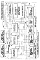
- the drawing shows a block diagram of a system according to an embodiment of the present invention.
- a memory access controller 1 is arranged between a main memory 2 which operates in synchronism with a second clock and arithmetic processors 3a to 3n (request sources of a memory request) which operate in synchronism with a first clock, and constituted by a memory request controller 13 which operates in synchronism with the second clock, data buffers lla to lln which operate in synchronism with the first clock and are provided in correspondence with the request sources, and a cache invalidation request controller 12.
- Each of the data buffers 11a to 11n provided in correspondence with the request sources can be accessed by two read addresses.
- the memory request controller 13 comprises a memory request information read circuit 131 for generating a data buffer address for reading out memory access information from the data buffers 11a to 11n provided in correspondence with the request sources, a request information accept register 132 for storing the readout data, a request identifying circuit 133 for identifying the type of instruction of a request, a data read address buffer 134 for storing a read address of a data buffer, and a cache invalidation request generator 135 for issuing a cache invalidation request for cache invalidation.
- the cache invalidation request controller 12 comprises a data buffer controller 121 for controlling the data buffers 11a to 11n provided in correspondence with the request sources, a cache invalidation data register 122 for storing a memory request address read out from the data buffer controller 121, and a cache invalidation discriminating circuit 123 for discriminating the presence/absence of a cache function of a request source.
- a memory request issued by the arithmetic processor 3a is supplied to the memory access controller 1 through a line L301, and memory access information supplied together with the memory request is stored in the data buffer 11a provided in the memory access controller 1 and corresponding to the request source.
- the memory request is sent to the memory request controller 13 which operates with the second clock and received by the memory request information read circuit 131.
- the memory request information read circuit 131 performs contention control for memory requests with the other arithmetic processors 3b to 3n. If the memory request can be processed, a data buffer address is generated in order to read out the memory access information from the data buffer lla corresponding to the memory request.
- the memory request information read circuit 131 sends the data buffer address to the data buffer 11a through a line L131.
- the memory access information read out from the data buffer is stored in the request information accept register 132 through a line L111.
- the memory access information stored in the request information accept register is sent together with the memory request to the main memory 2 through a line L134.
- the request identifying circuit 133 identifies the type of instruction of the memory request. If the instruction is a store instruction, the request identifying circuit 133 sends a valid signal to the cache invalidation request generator 135.
- the cache invalidation request generator 135 receives the valid signal and stores the data buffer address used to read out the memory access information from the data buffer 11a and the number of the data buffer corresponding to the memory request in the data read address buffer 134 in the order of sending the memory requests to the main memory 2.
- the cache invalidation request generator 135 sends a cache invalidation request to the data buffer controller 121 of the cache invalidation request controller 12 through a line L135.
- the data buffer controller 121 When the data buffer control 121 receives the cache invalidation request, the data buffer controller 121 generates a read address for reading out the data buffer address stored in the order of sending the memory access information to the main memory 2 and the number of the data buffer corresponding to the memory request from the data read address buffer 134 of the memory request controller 13, and supplies the read address to the data read address buffer 134 through a line L139, thereby reading out the data buffer address and the data buffer number.
- the data buffer controller 121 identifies the corresponding data buffer 11 in accordance with the data buffer number and supplies the data buffer addresses to the data buffer 11 through a line L121.
- the data buffer controller 121 reads out the corresponding memory request address and stores the readout address in the cache invalidation data register 122.
- the cache invalidation request is sent to the cache invalidation discriminating circuit 123.
- the cache invalidation discriminating circuit 123 discriminates the presence/absence of a cache function of a processor and sends the memory request address with the cache invalidation request to a processor having the cache function through a line L124.
- a data buffer address for reading out a memory request address from a data buffer which stores memory request information is stored in an additional data read address buffer.
- the data buffer address stored in this buffer is read out to access the data buffer, thereby reading out the main memory address for cache invalidation. Therefore, since no special buffer for storing the main memory address need be provided, a hardware amount can be decreased.
Landscapes
- Engineering & Computer Science (AREA)
- Theoretical Computer Science (AREA)
- Physics & Mathematics (AREA)
- General Engineering & Computer Science (AREA)
- General Physics & Mathematics (AREA)
- Memory System Of A Hierarchy Structure (AREA)
Claims (1)
- Informationsverarbeitungssystem mit:dadurch gekennzeichnet, daß die Cache-Annullierungssteuereinrichtung aufweist:einem Hauptspeicher (2);einer Anforderungsquelle (3a, ..., 3n), die eine Cache-Funktion haben kann, zum Erzeugen einer Speicheranforderung an den Hauptspeicher (2);einem Datenpuffer (11a, ..., 11n), der zwischen der Anforderungsquelle und dem Hauptspeicher vorgesehen ist, zum zeitweiligen Speichern von Speicheranforderungsinformationen von der Anforderungsquelle;einer Speicheranforderungs-Steuereinrichtung (13) zum Auslesen der Speicheranforderungsinformationen aus dem Datenpuffer, um einen Zugriff auf den Hauptspeicher durchzuführen und zu steuern, wobei die Speicheranforderungs-Steuereinrichtung einen Datenleseadreßpuffer (134) zum Speichern einer Speicherungsadresse der Speicheranforderungsinformationen in dem Datenpuffer aufweist; einer Cache-Annullierungssteuereinrichtung (12) zum Steuern einer Cache-Annullierungsverarbeitung bezüglich der Anforderungsquelle auf der Grundlage der Speicheranforderungsinformationen, wenn die Anforderungsquelle eine Cache-Funktion hat,eine Datenpuffer-Steuereinrichtung (121) zum Auslesen der Speicherungsadresse in dem Datenleseadreßpuffer (134), um auf den Datenpuffer zuzugreifen,eine Einrichtung zum Durchführen der Cache-Annullierungsverarbeitung bezüglich der Anforderungsquelle durch Verwendung einer Speicheranforderungsadresse der aus dem Datenpuffer (11) ausgelesenen Speicheranforderungsinformationen, undeine Cache-Annullierungsunterscheidungsschaltung (123) zum Unterscheiden des Vorhandenseins/Fehlens einer Cache-Funktion der Anforderungsquelle, wobei die Cache-Annullierungsunterscheidungsschaltung geeignet ist, eine Cache-Annullierungsanforderung über eine Leitung (L124) zu der Anforderungsquelle mit der Cache-Funktion zu senden.
Applications Claiming Priority (2)
| Application Number | Priority Date | Filing Date | Title |
|---|---|---|---|
| JP1265733A JPH0666056B2 (ja) | 1989-10-12 | 1989-10-12 | 情報処理システム |
| JP265733/89 | 1989-10-12 |
Publications (3)
| Publication Number | Publication Date |
|---|---|
| EP0422656A2 EP0422656A2 (de) | 1991-04-17 |
| EP0422656A3 EP0422656A3 (en) | 1992-07-22 |
| EP0422656B1 true EP0422656B1 (de) | 1998-01-21 |
Family
ID=17421243
Family Applications (1)
| Application Number | Title | Priority Date | Filing Date |
|---|---|---|---|
| EP90119527A Expired - Lifetime EP0422656B1 (de) | 1989-10-12 | 1990-10-11 | Informationsverarbeitungsanordnung |
Country Status (6)
| Country | Link |
|---|---|
| US (1) | US5251311A (de) |
| EP (1) | EP0422656B1 (de) |
| JP (1) | JPH0666056B2 (de) |
| AU (1) | AU640172B2 (de) |
| CA (1) | CA2027226C (de) |
| DE (1) | DE69031967T2 (de) |
Families Citing this family (56)
| Publication number | Priority date | Publication date | Assignee | Title |
|---|---|---|---|---|
| US5537574A (en) * | 1990-12-14 | 1996-07-16 | International Business Machines Corporation | Sysplex shared data coherency method |
| US5598551A (en) * | 1993-07-16 | 1997-01-28 | Unisys Corporation | Cache invalidation sequence system utilizing odd and even invalidation queues with shorter invalidation cycles |
| US5813028A (en) * | 1993-10-12 | 1998-09-22 | Texas Instruments Incorporated | Cache read miss request invalidation prevention method |
| EP0735481B1 (de) * | 1995-03-31 | 2003-05-14 | Sun Microsystems, Inc. | Mechanismus auf Systemebene zum Entwerten von Daten, die im externen Cache eines Prozessors in einem Computersystem gespeichert sind |
| GB2302604B (en) * | 1995-06-23 | 2000-02-16 | Advanced Risc Mach Ltd | Data memory access control |
| JP2731761B2 (ja) * | 1995-08-29 | 1998-03-25 | 甲府日本電気株式会社 | ネットワーク制御装置 |
| US8225002B2 (en) * | 1999-01-22 | 2012-07-17 | Network Disk, Inc. | Data storage and data sharing in a network of heterogeneous computers |
| US6590907B1 (en) | 1999-10-01 | 2003-07-08 | Stmicroelectronics Ltd. | Integrated circuit with additional ports |
| US6629115B1 (en) | 1999-10-01 | 2003-09-30 | Hitachi, Ltd. | Method and apparatus for manipulating vectored data |
| US6567932B2 (en) | 1999-10-01 | 2003-05-20 | Stmicroelectronics Limited | System and method for communicating with an integrated circuit |
| US6665816B1 (en) | 1999-10-01 | 2003-12-16 | Stmicroelectronics Limited | Data shift register |
| US6487683B1 (en) | 1999-10-01 | 2002-11-26 | Stmicroelectronics Limited | Microcomputer debug architecture and method |
| US6460174B1 (en) | 1999-10-01 | 2002-10-01 | Stmicroelectronics, Ltd. | Methods and models for use in designing an integrated circuit |
| US6412047B2 (en) | 1999-10-01 | 2002-06-25 | Stmicroelectronics, Inc. | Coherency protocol |
| US6502210B1 (en) | 1999-10-01 | 2002-12-31 | Stmicroelectronics, Ltd. | Microcomputer debug architecture and method |
| US6449712B1 (en) | 1999-10-01 | 2002-09-10 | Hitachi, Ltd. | Emulating execution of smaller fixed-length branch/delay slot instructions with a sequence of larger fixed-length instructions |
| US6557119B1 (en) | 1999-10-01 | 2003-04-29 | Stmicroelectronics Limited | Microcomputer debug architecture and method |
| US6779145B1 (en) | 1999-10-01 | 2004-08-17 | Stmicroelectronics Limited | System and method for communicating with an integrated circuit |
| US6826191B1 (en) | 1999-10-01 | 2004-11-30 | Stmicroelectronics Ltd. | Packets containing transaction attributes |
| US6928073B2 (en) * | 1999-10-01 | 2005-08-09 | Stmicroelectronics Ltd. | Integrated circuit implementing packet transmission |
| US6351803B2 (en) | 1999-10-01 | 2002-02-26 | Hitachi Ltd. | Mechanism for power efficient processing in a pipeline processor |
| US7260745B1 (en) | 1999-10-01 | 2007-08-21 | Stmicroelectronics Ltd. | Detection of information on an interconnect |
| US7000078B1 (en) | 1999-10-01 | 2006-02-14 | Stmicroelectronics Ltd. | System and method for maintaining cache coherency in a shared memory system |
| US6434665B1 (en) | 1999-10-01 | 2002-08-13 | Stmicroelectronics, Inc. | Cache memory store buffer |
| US6629207B1 (en) | 1999-10-01 | 2003-09-30 | Hitachi, Ltd. | Method for loading instructions or data into a locked way of a cache memory |
| US6530047B1 (en) | 1999-10-01 | 2003-03-04 | Stmicroelectronics Limited | System and method for communicating with an integrated circuit |
| US7793261B1 (en) | 1999-10-01 | 2010-09-07 | Stmicroelectronics Limited | Interface for transferring debug information |
| US6546480B1 (en) | 1999-10-01 | 2003-04-08 | Hitachi, Ltd. | Instructions for arithmetic operations on vectored data |
| US7072817B1 (en) * | 1999-10-01 | 2006-07-04 | Stmicroelectronics Ltd. | Method of designing an initiator in an integrated circuit |
| US6408381B1 (en) | 1999-10-01 | 2002-06-18 | Hitachi, Ltd. | Mechanism for fast access to control space in a pipeline processor |
| US6412043B1 (en) | 1999-10-01 | 2002-06-25 | Hitachi, Ltd. | Microprocessor having improved memory management unit and cache memory |
| JP2001142692A (ja) * | 1999-10-01 | 2001-05-25 | Hitachi Ltd | 2つの異なる固定長命令セットを実行するマイクロプロセッサ、マイクロコンピュータおよび命令実行方法 |
| US6598177B1 (en) | 1999-10-01 | 2003-07-22 | Stmicroelectronics Ltd. | Monitoring error conditions in an integrated circuit |
| US6574651B1 (en) | 1999-10-01 | 2003-06-03 | Hitachi, Ltd. | Method and apparatus for arithmetic operation on vectored data |
| US6820195B1 (en) | 1999-10-01 | 2004-11-16 | Hitachi, Ltd. | Aligning load/store data with big/little endian determined rotation distance control |
| US6684348B1 (en) | 1999-10-01 | 2004-01-27 | Hitachi, Ltd. | Circuit for processing trace information |
| US6633971B2 (en) | 1999-10-01 | 2003-10-14 | Hitachi, Ltd. | Mechanism for forward data in a processor pipeline using a single pipefile connected to the pipeline |
| US7266728B1 (en) | 1999-10-01 | 2007-09-04 | Stmicroelectronics Ltd. | Circuit for monitoring information on an interconnect |
| US6859891B2 (en) | 1999-10-01 | 2005-02-22 | Stmicroelectronics Limited | Apparatus and method for shadowing processor information |
| US6772325B1 (en) * | 1999-10-01 | 2004-08-03 | Hitachi, Ltd. | Processor architecture and operation for exploiting improved branch control instruction |
| US6601189B1 (en) | 1999-10-01 | 2003-07-29 | Stmicroelectronics Limited | System and method for communicating with an integrated circuit |
| US6457118B1 (en) | 1999-10-01 | 2002-09-24 | Hitachi Ltd | Method and system for selecting and using source operands in computer system instructions |
| US6542983B1 (en) | 1999-10-01 | 2003-04-01 | Hitachi, Ltd. | Microcomputer/floating point processor interface and method |
| US6349371B1 (en) | 1999-10-01 | 2002-02-19 | Stmicroelectronics Ltd. | Circuit for storing information |
| US6918065B1 (en) | 1999-10-01 | 2005-07-12 | Hitachi, Ltd. | Method for compressing and decompressing trace information |
| US6598128B1 (en) | 1999-10-01 | 2003-07-22 | Hitachi, Ltd. | Microprocessor having improved memory management unit and cache memory |
| US6732307B1 (en) | 1999-10-01 | 2004-05-04 | Hitachi, Ltd. | Apparatus and method for storing trace information |
| US6615370B1 (en) | 1999-10-01 | 2003-09-02 | Hitachi, Ltd. | Circuit for storing trace information |
| US6701405B1 (en) | 1999-10-01 | 2004-03-02 | Hitachi, Ltd. | DMA handshake protocol |
| US6463553B1 (en) | 1999-10-01 | 2002-10-08 | Stmicroelectronics, Ltd. | Microcomputer debug architecture and method |
| US6591369B1 (en) | 1999-10-01 | 2003-07-08 | Stmicroelectronics, Ltd. | System and method for communicating with an integrated circuit |
| US6298394B1 (en) | 1999-10-01 | 2001-10-02 | Stmicroelectronics, Ltd. | System and method for capturing information on an interconnect in an integrated circuit |
| US6553460B1 (en) | 1999-10-01 | 2003-04-22 | Hitachi, Ltd. | Microprocessor having improved memory management unit and cache memory |
| US6693914B1 (en) | 1999-10-01 | 2004-02-17 | Stmicroelectronics, Inc. | Arbitration mechanism for packet transmission |
| US6529968B1 (en) * | 1999-12-21 | 2003-03-04 | Intel Corporation | DMA controller and coherency-tracking unit for efficient data transfers between coherent and non-coherent memory spaces |
| JP4936251B2 (ja) * | 2007-03-27 | 2012-05-23 | パナソニック株式会社 | 風向変更グリル |
Family Cites Families (15)
| Publication number | Priority date | Publication date | Assignee | Title |
|---|---|---|---|---|
| US4467411A (en) * | 1981-03-06 | 1984-08-21 | International Business Machines Corporation | Scheduling device operations in a buffered peripheral subsystem |
| CA1187198A (en) * | 1981-06-15 | 1985-05-14 | Takashi Chiba | System for controlling access to channel buffers |
| US4622631B1 (en) * | 1983-12-30 | 1996-04-09 | Recognition Int Inc | Data processing system having a data coherence solution |
| US4835678A (en) * | 1985-02-01 | 1989-05-30 | Nec Corporation | Cache memory circuit for processing a read request during transfer of a data block |
| US5045996A (en) * | 1986-11-12 | 1991-09-03 | Xerox Corporation | Multiprocessor cache memory housekeeping |
| JPH0668735B2 (ja) * | 1987-02-09 | 1994-08-31 | 日本電気アイシーマイコンシステム株式会社 | キヤツシユメモリ− |
| US4851991A (en) * | 1987-02-24 | 1989-07-25 | Digital Equipment Corporation | Central processor unit for digital data processing system including write buffer management mechanism |
| US5091845A (en) * | 1987-02-24 | 1992-02-25 | Digital Equipment Corporation | System for controlling the storage of information in a cache memory |
| US5077658A (en) * | 1987-10-19 | 1991-12-31 | International Business Machines Corporation | Data access system for a file access processor |
| US4888681A (en) * | 1987-10-19 | 1989-12-19 | International Business Machines Corporation | Space management system for data files having shared access |
| US4888679A (en) * | 1988-01-11 | 1989-12-19 | Digital Equipment Corporation | Method and apparatus using a cache and main memory for both vector processing and scalar processing by prefetching cache blocks including vector data elements |
| EP0343567A3 (de) * | 1988-05-25 | 1991-01-09 | Hitachi, Ltd. | Mehrprozessoranordnung und Cache-Speichervorrichtung zur Verwendung in dieser Anordnung |
| US5148536A (en) * | 1988-07-25 | 1992-09-15 | Digital Equipment Corporation | Pipeline having an integral cache which processes cache misses and loads data in parallel |
| US4965717A (en) * | 1988-12-09 | 1990-10-23 | Tandem Computers Incorporated | Multiple processor system having shared memory with private-write capability |
| JP3338312B2 (ja) * | 1996-11-05 | 2002-10-28 | 日鉱金属株式会社 | 銅製錬用自溶炉の炉内付着物除去方法及び装置 |
-
1989
- 1989-10-12 JP JP1265733A patent/JPH0666056B2/ja not_active Expired - Fee Related
-
1990
- 1990-10-10 CA CA002027226A patent/CA2027226C/en not_active Expired - Fee Related
- 1990-10-11 EP EP90119527A patent/EP0422656B1/de not_active Expired - Lifetime
- 1990-10-11 AU AU64515/90A patent/AU640172B2/en not_active Ceased
- 1990-10-11 DE DE69031967T patent/DE69031967T2/de not_active Expired - Fee Related
- 1990-10-11 US US07/595,575 patent/US5251311A/en not_active Expired - Fee Related
Also Published As
| Publication number | Publication date |
|---|---|
| CA2027226A1 (en) | 1991-04-13 |
| EP0422656A3 (en) | 1992-07-22 |
| JPH0666056B2 (ja) | 1994-08-24 |
| JPH03127147A (ja) | 1991-05-30 |
| US5251311A (en) | 1993-10-05 |
| CA2027226C (en) | 1995-08-29 |
| AU640172B2 (en) | 1993-08-19 |
| DE69031967D1 (de) | 1998-02-26 |
| AU6451590A (en) | 1991-04-18 |
| DE69031967T2 (de) | 1998-05-20 |
| EP0422656A2 (de) | 1991-04-17 |
Similar Documents
| Publication | Publication Date | Title |
|---|---|---|
| EP0422656B1 (de) | Informationsverarbeitungsanordnung | |
| US4768148A (en) | Read in process memory apparatus | |
| KR100194253B1 (ko) | 메시 데이터 코히어런시 프로토콜 이용 방법 및 멀티프로세서 시스템 | |
| US4747043A (en) | Multiprocessor cache coherence system | |
| US4654790A (en) | Translation of virtual and real addresses to system addresses | |
| US5765196A (en) | System and method for servicing copyback requests in a multiprocessor system with a shared memory | |
| US4481573A (en) | Shared virtual address translation unit for a multiprocessor system | |
| JP3533355B2 (ja) | キャッシュ・メモリ・システム | |
| US4471429A (en) | Apparatus for cache clearing | |
| US4847804A (en) | Apparatus and method for data copy consistency in a multi-cache data processing unit | |
| EP0343567A2 (de) | Mehrprozessoranordnung und Cache-Speichervorrichtung zur Verwendung in dieser Anordnung | |
| KR100234503B1 (ko) | 디렉토리 기반의 캐시 코히어런스 프로토콜을 사용하는 멀티프로세서에서의 무효화 버스 최적화 | |
| US5426754A (en) | Cross-interrogate method and means for combined scaler and vector processing system | |
| US5479629A (en) | Method and apparatus for translation request buffer and requestor table for minimizing the number of accesses to the same address | |
| US5680577A (en) | Method and system for processing multiple requests for data residing at the same memory address | |
| WO1997004392A1 (en) | Shared cache memory device | |
| JPH07152647A (ja) | 共有メモリマルチプロセッサ | |
| US6931510B1 (en) | Method and system for translation lookaside buffer coherence in multiprocessor systems | |
| EP0153109B1 (de) | Cache-Kohärenz-Anordnung | |
| JP2002007371A (ja) | L1キャッシュフォールスシェア緩和制御方式 | |
| GB2233480A (en) | Multiprocessor data processing system | |
| JP3293872B2 (ja) | キャッシュ一致化方式 | |
| JPH07295881A (ja) | キャッシュ装置 | |
| JPH0336648A (ja) | 電子計算機及びtlb装置とマイクロプロセッサチップ | |
| JPH0836526A (ja) | 情報処理システム |
Legal Events
| Date | Code | Title | Description |
|---|---|---|---|
| PUAI | Public reference made under article 153(3) epc to a published international application that has entered the european phase |
Free format text: ORIGINAL CODE: 0009012 |
|
| 17P | Request for examination filed |
Effective date: 19901107 |
|
| AK | Designated contracting states |
Kind code of ref document: A2 Designated state(s): BE DE FR GB NL SE |
|
| PUAL | Search report despatched |
Free format text: ORIGINAL CODE: 0009013 |
|
| AK | Designated contracting states |
Kind code of ref document: A3 Designated state(s): BE DE FR GB NL SE |
|
| 17Q | First examination report despatched |
Effective date: 19960417 |
|
| GRAG | Despatch of communication of intention to grant |
Free format text: ORIGINAL CODE: EPIDOS AGRA |
|
| GRAG | Despatch of communication of intention to grant |
Free format text: ORIGINAL CODE: EPIDOS AGRA |
|
| GRAG | Despatch of communication of intention to grant |
Free format text: ORIGINAL CODE: EPIDOS AGRA |
|
| GRAH | Despatch of communication of intention to grant a patent |
Free format text: ORIGINAL CODE: EPIDOS IGRA |
|
| GRAH | Despatch of communication of intention to grant a patent |
Free format text: ORIGINAL CODE: EPIDOS IGRA |
|
| GRAG | Despatch of communication of intention to grant |
Free format text: ORIGINAL CODE: EPIDOS AGRA |
|
| GRAA | (expected) grant |
Free format text: ORIGINAL CODE: 0009210 |
|
| AK | Designated contracting states |
Kind code of ref document: B1 Designated state(s): BE DE FR GB NL SE |
|
| REF | Corresponds to: |
Ref document number: 69031967 Country of ref document: DE Date of ref document: 19980226 |
|
| ET | Fr: translation filed | ||
| PLBE | No opposition filed within time limit |
Free format text: ORIGINAL CODE: 0009261 |
|
| STAA | Information on the status of an ep patent application or granted ep patent |
Free format text: STATUS: NO OPPOSITION FILED WITHIN TIME LIMIT |
|
| 26N | No opposition filed | ||
| REG | Reference to a national code |
Ref country code: GB Ref legal event code: IF02 |
|
| PGFP | Annual fee paid to national office [announced via postgrant information from national office to epo] |
Ref country code: BE Payment date: 20020917 Year of fee payment: 13 |
|
| PGFP | Annual fee paid to national office [announced via postgrant information from national office to epo] |
Ref country code: FR Payment date: 20021008 Year of fee payment: 13 |
|
| PGFP | Annual fee paid to national office [announced via postgrant information from national office to epo] |
Ref country code: SE Payment date: 20021009 Year of fee payment: 13 Ref country code: GB Payment date: 20021009 Year of fee payment: 13 |
|
| PGFP | Annual fee paid to national office [announced via postgrant information from national office to epo] |
Ref country code: DE Payment date: 20021017 Year of fee payment: 13 |
|
| PGFP | Annual fee paid to national office [announced via postgrant information from national office to epo] |
Ref country code: NL Payment date: 20021031 Year of fee payment: 13 |
|
| PG25 | Lapsed in a contracting state [announced via postgrant information from national office to epo] |
Ref country code: GB Free format text: LAPSE BECAUSE OF NON-PAYMENT OF DUE FEES Effective date: 20031011 |
|
| PG25 | Lapsed in a contracting state [announced via postgrant information from national office to epo] |
Ref country code: SE Free format text: LAPSE BECAUSE OF NON-PAYMENT OF DUE FEES Effective date: 20031012 |
|
| PG25 | Lapsed in a contracting state [announced via postgrant information from national office to epo] |
Ref country code: BE Free format text: LAPSE BECAUSE OF NON-PAYMENT OF DUE FEES Effective date: 20031031 |
|
| BERE | Be: lapsed |
Owner name: *NEC CORP. Effective date: 20031031 |
|
| PG25 | Lapsed in a contracting state [announced via postgrant information from national office to epo] |
Ref country code: NL Free format text: LAPSE BECAUSE OF NON-PAYMENT OF DUE FEES Effective date: 20040501 Ref country code: DE Free format text: LAPSE BECAUSE OF NON-PAYMENT OF DUE FEES Effective date: 20040501 |
|
| EUG | Se: european patent has lapsed | ||
| GBPC | Gb: european patent ceased through non-payment of renewal fee |
Effective date: 20031011 |
|
| PG25 | Lapsed in a contracting state [announced via postgrant information from national office to epo] |
Ref country code: FR Free format text: LAPSE BECAUSE OF NON-PAYMENT OF DUE FEES Effective date: 20040630 |
|
| NLV4 | Nl: lapsed or anulled due to non-payment of the annual fee |
Effective date: 20040501 |
|
| REG | Reference to a national code |
Ref country code: FR Ref legal event code: ST |